Note: Descriptions are shown in the official language in which they were submitted.
CA 02375539 2001-11-27
SEI 99-41
DESCRIPTION
OPTICAL AMPLIFIER AND OPTICAL AMPLIFICATION METHOD
Technical Field
The present invention relates to an optical
S amplifier and optical amplification method of
amplifying, at once, a multiplexed signal in which a
plurality of signal light components having different
wavelengths belonging to a predetermined wavelength
band are multiplexed.
Background Art
The optical amplifier which amplifies signal light
by guiding to a waveguide doped with a fluorescent
material together with optical pumping light of such
fluorescent material is well known. Such an optical
amplifier is provided in a relay station in an optical
transmission system. Especially, an optical amplifier
used in a wavelength-multiplexed transmission system
for transmitting multiplexed signal light in which a
plurality of signal light components having different
wavelengths are multiplexed optically must amplify the
plurality of signal light components at once at an
equal gain, and also amplify the power of each of the
plurality of signal light components to a predetermined
target value and output the signal light.
For example, reference 1, K. moue, et al.,
"Tunable Gain Equalization Using a Mach-Zehnder Optical
1
CA 02375539 2001-11-27
SEI 99-41
Fiber in Multistage Fiber Amplifiers", IEEE Photonics
Technology Letters, Vol. 3, No. 8, pp. 718 - 720 (1991)
is disclosed a technique of flattening the gain of an
optical amplifier by an optical fiber using a
Mach-Zehnder interferometer. Reference 2, S. Kinoshita,
et al., "Large Capacity WDM Transmission Based on
Wideband Erbium-Doped Fiber Amplifiers", OSA TOPS,
Vol. 25, pp. 258 - 261 (1998) is disclosed a technique
in which an optical attenuator with a variable
attenuation factor is inserted between the input-side
optical amplification section and the output-side
optical amplification section of an optical amplifier
so as to maintain constant power of signal light input
to the output-side optical amplification section even
when the power of signal light input to the input-side
optical amplification section varies, thereby
maintaining the power of signal light output from the
optical amplifier at a~predetermined target value and
simultaneously maintaining constant gain deviation of
the entire optical amplifier.
Disclosure of the Invention
In the technique described in reference 1, however,
for example, to keep the power of signal light output
from the optical amplifier at a predetermined target
value when the loss in the input-side transmission line
of the optical amplifier varies due to some reason, and
2
CA 02375539 2001-11-27
SEI 99-41
the power of signal light input to the optical
amplifier varies, the gain of optical amplification of
signal light in the optical amplifier must be changed.
If the gain is changed, the wavelength dependence of
gain varies. This damages the gain flatness of the
optical amplifier, and the plurality of signal light
components output from the optical amplifier have
different powers or so-called deviation.
In the technique described in reference 2, to keep
the power of signal light input to the output-side
optical amplification section at a predetermined target
value by the optical attenuator when the signal light
input to the input-side optical amplification section
has sufficiently high power, the power must be largely
attenuated by the optical attenuator. As a result, the
pumping efficiency lowers to degrade the noise factor.
The present invention has been made to solve the
above problems, and has as its object to provide an
optical amplifier and optical amplification method
capable of maintaining the output signal light power
and gain flatness without degrading the noise factor
even when the input signal light power varies.
In order to achieve the above object, according to
the present invention, there is provided an optical
amplifier for amplifying, at once, multiplexed signal
light belonging to a predetermined wavelength band, in
3
CA 02375539 2001-11-27
SEI 99-41
which a plurality of signal light components having
different wavelengths are multiplexed, characterized by
comprising (1) one or a plurality of optical
amplification sections each of which has an optical
waveguide doped with a fluorescent material and
amplifies the multiplexed signal light by optical
pumping of the fluorescent material, (2) an optical
pumping light source for supplying predetermined
optical pumping light to the optical amplification
section, (3) an optical filter capable of changing a
gradient dL/c~, of a loss L (dB) with respect to a
wavelength ~ (nm) in the predetermined wavelength band,
and (4) control means for controlling an optical
pumping light output from the optical pumping light
source such that light power after amplification has a
predetermined target value, and for adjusting a
characteristic of the optical filter to adjust a final
gain characteristic.
On the other hand, an optical amplification method
according to the present invention is characterized by
comprising the steps of (1) guiding the multiplexed
signal light to an optical waveguide doped with a
fluorescent material together with predetermined
optical pumping light and optically amplifying the
multiplexed signal light, (2) guiding at least one of
the multiplexed signal light before amplification and
4
CA 02375539 2001-11-27
SEI 99-41
that after amplification to an optical filter capable
of changing a gradient dL/d~, of a loss L (dB) with
respect to a wavelength ~, (nm) in the predetermined
wavelength band and adjusting the gradient dL/d~. of the
optical filter to reduce a wavelength-dependent gain in
the optical amplification, and (3) adjusting an
intensity of the optical pumping light to adjust light
power after amplification to a predetermined target
value.
According to the optical amplifier or optical
amplification method of the present invention, even
when the input signal light power to the optical
amplifier varies, the output signal light power from
the optical amplifier can be maintained at a
predetermined target value. In addition, even when the
gain of the optical amplification section has a
wavelength dependence due to variation in input signal
light power, the gain flatness of the entire optical
amplifier can be maintained by adjusting the gradient
dL/d~, of the loss L of the optical filter with respect
to the wavelength ~..
. This optical filter preferably satisfies
Laa(~.-~.c) +b
(where ~.c (nm) and b (dB) are constants) in the
predetermined wavelength band and changes a (dB/nm) to
adjust the gradient dL/d~.. Such an optical filter can
5
CA 02375539 2001-11-27
SEI 99-41
easily adjust the gradient dL/d~. When ~c is set in the
predetermined wavelength band, the loss L at the
wavelength ~c in the predetermined wavelength band
always becomes constant. This enables design with an
emphasis on the noise characteristic at ~c.
The optical amplifier may further comprise a gain
equalizer for compensating for a inherent wavelength-
dependent gain of the optical amplification section.
In this case, the gain equalizer equalizes the inherent
wavelength-dependent gain of the optical amplification
section, and the optical filter compensates for
variation in input multiplexed signal light power.
This makes the gain flatness of the entire optical
amplifier more excellent and facilitates
control/adjustment.
Preferably, the optical amplifier further
comprises a wave number monitor for detecting the
number of signal light components contained in the
multiplexed signal light, and the control means adjusts
the target value of light power after amplification in
accordance with the number of signal light components
detected by the wave number monitor. Even when the
power of input multiplexed signal light varies due to
an increase/decrease in the number of signal light
components, the power of each multiplexed signal light
component can be maintained constant.
6
CA 02375539 2001-11-27
SEI 99-41
The gradient dL/d~ of the optical filter may be
adjusted, e.g., 1) on the basis of the detection result
from input light power detection means for detecting
the light power input to the optical amplification
section, 2) on the basis of the detection result from
gain detection means for detecting a gain of the
optical amplification section, 3) on the basis of power
deviation between shortest and longest wavelengths
detected by detecting each wavelength and power of
signal light components contained in the light output
from the optical amplification section, or 4) such that
a level difference between ASE light levels detected by
ASE light level detection means for detecting an ASE
light level of each of wavelengths outside two ends of
the predetermined wavelength band of the light output
from the optical amplification section. Each
wavelength and power of signal light components
contained in the light output from the optical
amplification section may be detected, and an ASE light
level of a wavelength at a shorter wavelength than
detected shortest wavelength and at a longer wavelength
than detected longest wavelength may be detected and
used for adjustment. In case 3) or 4), a wavelength
for which the power deviation or ASE .light level is to
be detected may be determined on the basis of
information related to the shortest and longest
7
CA 02375539 2001-11-27
SEI 99-41
wavelengths, which are sent together with the
multiplexed signal light.
In addition, when a total transmittance in the
predetermined wavelength band of the optical filter is
adjusted to a maximum value, the loss L is preferably
adjusted to be substantially constant independently of
the wavelength. This enables to reduce the noise
factor especially when the input multiplexed signal
light power is small.
Any one of the above arrangements and methods
facilitates adjustment of the gradient dL/d3~, of the
optical filter and realizes the object of the present
invention.
The optical filter in the optical amplifier
according to the present invention preferably comprises
(1) a main optical path which guides the multiplexed
signal light and is divided into first to sixth regions
sequentially from an upstream side, (2) a first sub
optical path which is arranged close to the first and
third regions of the main optical path so that optical
coupling of propagation light occurs, is spaced apart
from the second region of the main optical path so that
optical coupling of the propagation light does not
occur, and has a region corresponding to the second
region of the main optical path, the region having a
length different from that of the main optical path,
8
CA 02375539 2001-11-27
SEI 99-41
(3) a second sub optical path which is arranged close
to the fourth and sixth regions of the main optical
path so that optical coupling of the propagation light
occurs, is spaced apart from the fifth region of the
main optical path so that optical coupling of the
propagation light does not occur, and has a region
corresponding to the fifth region of the main optical
path, the region having a length different from that of
the main optical path, (4) a first temperature
adjusting device arranged in at least one of the second
region of the main optical path and the region of the
first sub optical path, which corresponds to the second
region of the main optical path, and (5) a second
temperature adjusting device arranged in at least one
of the fifth region of the main optical path and the
region of the second sub optical path, which
corresponds to the fifth region of the main optical
path.
On the other hand, in the optical amplification
method according to the present invention, preferably,
an optical filter comprising (1) a main optical path
which guides the multiplexed signal light and is
divided into first to sixth regions sequentially from
an upstream side, (2) a first sub optical path which is
arranged close to the first and third regions of the
main optical path so that optical coupling of
9
CA 02375539 2001-11-27
SEI 99-41
propagation light occurs, is spaced apart from the
second region of the main optical path so that optical
coupling of the propagation light does not occur, and
has a region corresponding to the second region of the
main optical path, the region having a length different
from that of the main optical path, and (3) a second
sub optical path which is arranged close to the fourth
and sixth regions of the main optical path so that
optical coupling of the propagation light occurs, is
spaced apart from the fifth region of the main optical
path so that optical coupling of the propagation light
does not occur, and has a region corresponding to the
fifth region of the main optical path, the region
having a length different from that of the main optical
path is used, and the gain wavelength dependence
reduction step comprises adjusting at least one of a
temperature in the first sub optical path and a
temperature in a region of the main optical path, which
corresponds to the first sub optical path, and at least
one of a temperature in the second sub optical path and
a temperature in a region of the main optical path,
which corresponds to the second sub optical path to
adjust the gradient dL/d~ of the optical filter.
Each of the first and second sub optical paths and
the corresponding main optical path form a Mach-Zehnder
interference device. In each Mach-Zehnder interference
CA 02375539 2001-11-27
SEI 99-41
device, when the temperature of at least one of the
optical paths is adjusted, the wavelength dependence of
loss in each main optical path can be adjusted. Hence,
this optical filter is suitable for the optical
amplifier and optical amplification method according to
the present invention.
Brief Description of the Drawings
Fig. 1 is a schematic view showing the arrangement
of an optical amplifier according to the first
embodiment of the present invention;
Fig. 2 is an explanatory view of the output-side
optical amplification section and optical pumping light
source, and Fig. 3 is an explanatory view of the
optical filter;
Figs. 4 to 6 are graphs showing loss spectra
obtained when a phase value e~ was changed in Examples A
to C of the optical filter;
Figs. 7A to 7D are views for explaining the
operation of the optical amplifier according to the
first embodiment;
Figs. 8, 9, and 10A are schematic views showing
the arrangements of optical amplifiers according to the
second to fourth embodiments of the present invention,
respectively, and Fig. 10B is a schematic view showing
the arrangement of a modification of the fourth
embodiment;
11
CA 02375539 2001-11-27
SEI 99-41
Fig. 11 is an explanatory view of an optical
filter and spectrum monitor device in the third
embodiment;
Fig. 12 is a schematic view showing the
arrangement of an optical amplifier according to the
fifth embodiment of the present invention, and
Figs. 13A to 13C are views for explaining its
operation;
Figs. 14A and 14B are schematic views showing the
arrangements of an optical amplifier according to the
sixth embodiment of the present invention and its
modification, respectively, Fig. 15 is a schematic view
showing the arrangement of an optical amplifier
according to the seventh embodiment of the present
invention, and Fig. 16 is a graph which compares the
noise characteristic of the seventh embodiment with
that of a conventional optical amplifier;
Fig. 17 is a view for explaining the loss spectrum
of a modification of an optical filter used in the
optical amplifier according to the present invention;
and
Fig. 18 is a schematic view showing the
arrangement of an optical amplifier according to the
eighth embodiment of the present invention.
Best Modes for Carrying Out the Invention
12
CA 02375539 2001-11-27
SEI 99-41
Preferred Embodiments of the present invention
will be described below in detail with reference to the
accompanying drawings. To facilitate the
comprehension of the explanation, the same reference
numerals denota the same parts, where possible,
throughout the drawings, and a repeated explanation
will be omitted.
(First Embodiment)
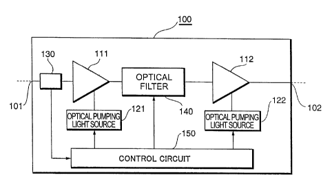
Fig. 1 is a schematic view of an optical amplifier
according to the first embodiment. In the optical
amplifier 100 according to this embodiment, an optical
coupler 130, input-side optical amplification section
111, optical filter 140, and output-side optical
amplification section 112 are sequentially connected in
series between an optical input terminal 101 and an
optical output terminal 102. The optical amplifier 100
also has optical pumping light sources 121 and 122 for
supplying optical pumping light to the input-side
optical amplification section 111 and output-side
optical amplification section 112, respectively, and a
control circuit 150 for controlling the light powers
from the optical pumping light sources 121 and 122 and
the loss spectrum of the optical filter 140.
The optical coupler 130 demultiplexes some
components of multiplexed signal light input to the
optical input terminal 101, outputs the components to
13
CA 02375539 2001-11-27
SEI 99-41
the control circuit 150, and outputs the remaining
components to the input-side optical amplification
section 111. The input-side optical amplification
section 111 receives optical pumping light from the
optical pumping light source 121, optically amplifies
the multiplexed signal light sent from the optical
coupler 130 at once, and outputs the signal light. The
optical filter 140 has a loss spectrum in which the
total loss is almost constant in the wavelength band of
the multiplexed signal light, and the gradient of loss
with respect to the wavelength is variable in the
wavelength band. The output-side optical amplification
section 112 receives optical pumping light from the
optical pumping light source 122, optically amplifies
the multiplexed signal light sent from the optical
filter 140 at once, and outputs the signal light to the
optical output terminal 102.
The control circuit 150 detects the power of
multiplexed signal light demultiplexed by the optical
coupler 130. The control circuit 150 controls the
power of optical pumping light to be output from the
optical pumping light sources 121 and 122 on the basis
of the power of input multiplexed signal light such
that the power of output multiplexed signal light
obtains a predetermined target value. The control
circuit 150 also controls the loss spectrum of the
14
CA 02375539 2001-11-27
SEI 99-41
optical filter 140 on the basis of the power of input
multiplexed signal light.
Fig. 2 is an explanatory view of the input-side
optical amplification section 111 and optical pumping
light source 121. The input-side optical amplification
section 111 includes an amplification optical fiber 113,
optical coupler 114, and optical isolators 115 and 116.
The optical coupler 114 sends optical pumping light
output from the optical pumping light source 121 to the
amplification optical fiber 113 and also passes signal
light output from the amplification optical fiber 113.
The optical isolators 115 and 116 pass light in the
forward direction but do not pass light in the reverse
direction.
The amplification optical fiber 113 is an optical
waveguide doped with a fluorescent material that can be
excited by optical pumping light output from the
optical pumping light source 121. The fluorescent
material to be doped is preferably a rare earth element
and, more preferably, Er. Er is preferably doped
because signal light in a 1.55-N.m band can be optically
amplified. At this time, the wavelength of optical
pumping light to be output from the optical pumping
light source 121 and supplied to the amplification
optical fiber 113 is preferably 1.48 N,m or 0.98 Vim.
The output-side optical amplification section 112 and
CA 02375539 2001-11-27
SEI 99-41
optical pumping light source 122 have the same
arrangement as described above.
A preferred example of the optical filter 140 will
be described next. Fig. 3 is an explanatory view of
the optical filter 140. This optical filter 140 is a
planar lightwave circuit formed on a substrate 10 made
of, e.g., quartz, and comprises a main optical path 20,
first sub optical path 21, second sub optical path 22,
heater 51 serving as a first temperature adjustment
means, and heater 53 serving as a second temperature
adjustment means.
The main optical path 20 is an optical waveguide
for guiding light incident on an optical input terminal
11 at one end face of the substrate 10 to an optical
output terminal 12 at the other end face of the
substrate 10 and causes the light to emerge therefrom.
The main optical path 20 has six regions A to F.
The main optical path 20 and first sub optical
path 21 are close and optically coupled to each other
in the first region A and third region C, thereby
forming a first optical coupler 31 and second optical
coupler 32. In the second region B, the optical path
length of the main optical path 20 is set to be longer
than that of the first sub optical path 21, so the two
optical paths are spaced apart from each other. Thus,
the portion of the main optical path from the first
16
CA 02375539 2001-11-27
SEI 99-41
region A to the third region C and the first sub
optical path 21 construct an asymmetrical Mach-Zehnder
interference circuit. This portion will be referred to
as a first Mach-Zehnder interference circuit 41
hereinafter.
Similarly, the main optical path 20 and second sub
optical path 22 are close and optically coupled to each
other in the fourth region D and sixth region F,
thereby forming a third optical coupler 33 and fourth
optical coupler 34. In the fifth region E, the optical
path length of the main optical path 20 is set to be
shorter than that of the first sub optical path 21, so
the two optical paths are spaced apart from each other.
Thus, the portion of the main optical path from the
fourth region D to the sixth region F and the second
sub optical path 22 construct an asymmetrical
Mach-Zehnder interference circuit. This portion will
be referred to as a second Mach-Zehnder interference
circuit 42 hereinafter.
The heater 51 is formed on the second region B of
the main optical path 20. This heater 51 adjusts the
temperature of the main optical path 20 to adjust the
optical path length difference between the main optical
path 20 and the first sub optical path 21 in the first
Mach-Zehnder interference circuit 41, thereby adjusting
the transmission characteristic of the first
17
CA 02375539 2001-11-27
SEI 99-41
Mach-Zehnder interference circuit 41. The heater 53 is
formed on the fifth region E of the main optical path
20. This heater 53 adjusts the temperature of the main
optical path 20 to adjust the optical path length
difference between the main optical path 20 and the
second sub optical path 22 in the second Mach-Zehnder
interference circuit 42, thereby adjusting the
transmission characteristic of the second Mach-Zehnder
interference circuit 42. The heaters 51 and 53 are
controlled by the control circuit 150.
Heaters may be provided on the second region B of
the first sub optical path 21 and on the fifth region E
of the second sub optical path 22 in place of the
heaters 51 and 53. Alternatively, heaters may be
provided on both the main optical path and the first
and second sub optical paths. Instead of the heaters,
Peltier elements for cooling may be provided.
In this optical filter 1, a loss spectrum L(~)
[dB] for light input to the optical input terminal 11
and output from the optical output terminal 12 through
the main optical path 20 depend on both a transmittance
characteristic T1(~) of the first Mach-Zehnder
interference circuit 41 based on optical coupling
between the main optical path 20 and the first sub
optical path 21 by the optical couplers 31 and 32 and a
transmittance characteristic T1(~) of the second
18
CA 02375539 2001-11-27
SEI 99-41
Mach-Zehnder interferometer 42 based on optical
coupling between the main optical path 20 and the
second sub optical path 22 by the optical couplers 33
and 34.
Generally, a transmittance characteristic T(~.) of
an asymmetrical Mach-Zehnder interference circuit is
given by
T(~.)=1-AsinZ~~~e~~'°)+e~~ ~ (1)
where ~. [nm] is the wavelength of light, A, ~,o [nm] , and
e~, [nm] are constants determined by the structural
parameters of the Mach-Zehnder interference circuit,
and e~ is the phase value that can be set by temperature
adjustment. A loss spectrum L(~.) of the optical filter
1 is given by
L(~.) _ -101og{Ti ~~)' Ti ~~)} ( 2 )
A gradient dL (~.) /da, of the loss spectrum L (~.) of the
optical filter 1 with respect to the wavelength will be
simply referred to as a gradient S(~.) hereinafter.
When the constants A, ~.o, and e~, of each of the
first Mach-Zehnder interference circuit 41 and second
Mach-Zehnder interference circuit 42 are appropriately
designed, and the phase value e~ is changed by
temperature adjustment by the heaters 51 and 53 while
maintaining an almost constant loss L(~,1) at a
predetermined wavelength ~.1 in a predetermined
19
CA 02375539 2001-11-27
SEI 99-41
wavelength band, the loss L(~) and gradient S(~) in the
wavelength band can be changed. As will be described
later, the gradient S(~) of the optical filter 1 has
small dependence on the wavelength ~, and the linearity
of the loss L(~) of the optical filter 1 with respect
to the wavelength ~ is excellent.
The present inventor prepared several types of
optical filters 1 by changing the structural parameters
of the Mach-Zehnder interferometers 41 and 42 and
confirmed the variability of the gradient S(~). The
result will be described below.
A table below show the structural parameters in
examples.
Example _Example Example
A B C
First A 0.60 0.85 0.60
Mach-Zehnder ~ 1550 1550 1590
I ~
f
nter 200 200 200
erence ~'
Circuit
Second A 0.50 0.60 0.5
Mach-Zehnder ~,0 1600 1600 1640
I
f
nter ~ 200 200 200
erence
Circuit
In the optical filters of all examples, the
optical path lengths in the Mach-Zehnder interference
circuits 41 and 42 were set to 12.5~.o and 9.5~,o at
reference temperature. Under these conditions, the
heaters 51 and 53 were operated to adjust the
temperatures in the second region B and fifth region E
of the main optical path 20, respectively, thereby
changing the phase values A~ of the Mach-Zehnder
CA 02375539 2001-11-27
SEI 99-41
interference circuits 41 and 42 within the range of 0
rad to 0.595 rad such that the phase values had
opposite signs and equal absolute values.
Figs. 4 to 6 are graphs showing loss spectra
obtained when the phase value 0~ was changed in the
optical filters of Examples A to C.
As is apparent from Fig. 4, in Example A, the loss
ranges from 2.37 to 3.01 dB, i.e., is almost constant
near the central wavelength of 1,550 nm in the
wavelength band of 1,535 to 1,565 nm, and the gradient
S(~) can be set within the range of 0 to 5.05 dB/30 nm
in the wavelength band. When the phase value ~~ is
0.595 rad, the maximum value of the deviation from a
straight line passing through a point corresponding to
a loss of 2.89 dB (@central wavelength: 1,550 nm) is
sufficiently as small as ~0.21 dB. Thus, it was
confirmed that the gradient S(~) is excellent in
linearity.
As is apparent from Fig. 5, in Example B, the loss
ranges from 3.65 to 3.98 dB, i.e., is almost constant
near the central wavelength of 1,550 nm in the
wavelength band of 1,535 to 1,565 nm, and the gradient
S(~) can be set within the range of 0 to l0 dB/30 nm in
the wavelength band. When the phase value ~~ is 0.314
rad, the maximum value of the deviation from a straight
line passing through a point corresponding to a loss of
21
CA 02375539 2001-11-27
SEI 99-41
0.87 dB (@central wavelength: 1,550 nm) is sufficiently
as small as ~0.87 dB. Thus, it was confirmed that the
gradient S(~) is excellent in linearity.
As is apparent from Fig. 6, in Example C, the loss
ranges from 2.73 to 3.01 dB, i.e., is almost constant
near the central wavelength of 1,590 nm in the
wavelength band of 1,575 to 1,605 nm, and the gradient
S(~) can be set within the range of 0 to 5 dB/30 nm in
the wavelength band. When the phase value 0~ is 0.595
rad, the maximum value of the deviation from a straight
line passing through a point corresponding to a loss of
2.89 dB (@central wavelength: 1,590 nm) is sufficiently
as small as ~0.21 dB. Thus, it was confirmed that the
gradient S(~) is excellent in linearity.
When the structural parameters of the Mach-Zehnder
interference circuits 41 and 42 are appropriately set
such that the phase value ~~ is set to 0 by adjusting
the temperatures in the second region B and fifth
region E of the main optical path 20 to predetermined
bias temperatures, the phase value ~~ can be changed
within the range of 0 to +0.595 rad by making the
temperatures in the second region B and fifth region E
of the main optical path 20 higher than the bias
temperatures. In addition, the phase value ~~ can be
changed within the range of -0.595 to 0 rad by making
the temperatures in the second region B and fifth
22
CA 02375539 2001-11-27
SEI 99-41
region E of the main optical path 20 lower than the
bias temperatures. When the phase value 0~ is changed
within the range of -0.595 to +0.595 rad, the gradient
S(~) can be set within the range of ~ a dB/nm in a
predetermined wavelength band.
When Peltier elements are used in place of the
heaters 51 and 53 to raise or lower the temperatures in
the second region B and fifth region E of the main
optical path 20, the phase value 0~ can be set not only
to a positive value but also to a negative value. This
also makes it possible to change the phase value
within the range of -0.595 to +0.595 rad.
As described above, in the optical filter 140
shown in Fig. 3, the loss spectrum for light input to
the optical input terminal 11 and output from the
optical output terminal 12 through the main optical
path 20 is determined by the transmittance
characteristic of the first Mach-Zehnder interference
circuit 41 based on optical coupling between the main
optical path 20 and the first sub optical path 21 by
the optical couplers 31 and 32 and the transmittance
characteristic of the second Mach-Zehnder
interferometer 42 based on optical coupling between the
main optical path 20 and the second sub optical path 22
by the optical couplers 33 and 34. This optical filter
140 is preferable because it is integrated on the
23
CA 02375539 2001-11-27
SEI 99-41
substrate 10 and has a compact structure and also
because of its small insertion loss.
Operation of the optical amplifier 100 according
to the first embodiment will be described next, and an
optical amplifier control method according to the first
embodiment will be described. Figs. 7A to 7D are views
for explaining operation of the optical amplifier 100
according to the first embodiment. As for the loss
spectrum (Fig. 7A) of the optical filter 140, as
described above, the loss L(~i) is almost constant at
the predetermined wavelength ~i in the wavelength band
of signal light, and the gradient S(~) is variable in
the wavelength band. The gradient S(~) is controlled
by the control circuit 150 which monitors the input
signal light power.
Assume that the input signal light power has a
predetermined value, and the gain of optical
amplification of signal light by the input-side optical
amplification section 111 and output-side optical
amplification section 112 is almost constant
independently of the wavelength (Fig. 7B). In this
case, when the input signal light power becomes smaller
than the predetermined value, the gain of optical
amplification of signal light by the input-side optical
amplification section 111 and output-side optical
amplification section 112 is controlled by the control
24
CA 02375539 2001-11-27
SEI 99-41
circuit 150 and becomes large. As a consequence, the
longer the wavelength is, the smaller the gain becomes:
the gain has wavelength dependence (Fig. 7C). At this
time, however, the gradient S(~) of the optical filter
140 is controlled by the control circuit 150. The
longer the wavelength is, the smaller the loss is set.
Hence, the wavelength dependence of gain of the
input-side optical amplification section 111 and
output-side optical amplification section 112 is
canceled by the wavelength dependence of loss of the
optical filter 140. As a result, the gain
characteristic of the entire optical amplifier 100
becomes almost constant independently of the wavelength,
and the gain flatness is maintained (Fig. 7D).
As described above, in this embodiment, even when
the input signal light power varies, the output signal
light power can be maintained at a predetermined target
value, and the gain flatness of the entire optical
amplifier 100 can be maintained. In addition, since
the loss of the optical filter 140 is almost constant
at a predetermined wavelength in the wavelength band of
signal light, the noise factor does not degrade. In
this embodiment, the optical filter 140 may be located
on the output side of the output-side optical
amplification section 112.
(Second Embodiment)
CA 02375539 2001-11-27
SEI 99-41
Fig. 8 is a schematic view showing the arrangement
of an optical amplifier 200 according to the second
embodiment of the present invention. Fig. 8 also
illustrates an optical amplifier 200A provided on the
input side of the optical amplifier 200. In the
optical amplifier 200 according to this embodiment, an
optical coupler 230, input-side optical amplification
section 211, optical filter 240, and output-side
optical amplification section 212 are sequentially
connected in series between an optical input terminal
201 and an optical output terminal 202. The optical
amplifier 200 also has optical pumping light sources
221 and 222 for supplying optical pumping light to the
input-side optical amplification section 211 and
output-side optical amplification section 212,
respectively, and a control circuit 250 for controlling
the optical pumping light sources 221 and 222 and the
loss spectrum of the optical filter 240.
The arrangement of each element is the same as in
the first embodiment except the control circuit 250.
The control circuit 250 detects the power of input
signal light demultiplexed by the optical coupler 230,
as in the first embodiment, and also receives
information related to the power of signal light output
from the optical amplifier~200A on the input side,
which is transmitted from the optical amplifier 200A on
26
CA 02375539 2001-11-27
SEI 99-41
the input side. The control circuit 250 calculates the
necessary gain on the basis of the output signal light
power of the input-side optical amplifier 200A and the
input signal light power of the optical amplifier of
its own and controls the powers of optical pumping
light to be output from the optical pumping light
sources 221 and 222 such that the power of output
signal light has a predetermined target value. The
control circuit 250 also controls the loss spectrum of
the optical filter 240 on the basis of the necessary
gain.
More specifically, when the necessary gain becomes
large, the gain of optical amplification of signal
light by the input-side optical amplification section
211 and output-side optical amplification section 212
becomes smaller as the wavelength becomes long; the
gain has wavelength dependence. At this time, however,
the gradient S(~) of the optical filter 240 is
controlled by the control circuit 250 so that the
longer the wavelength is, the smaller the loss becomes.
Hence, the wavelength dependence of gain of the
input-side optical amplification section 211 and
output-side optical amplification section 212 is
canceled by the loss spectrum of the optical filter 240.
As a result, the gain characteristic of the entire
optical amplifier 200 becomes almost constant
27
CA 02375539 2001-11-27
SEI 99-41
independently of the wavelength, and the.gain flatness
is maintained.
As described above, in this embodiment as well,
even when the input signal light power varies, the
output signal light power can be maintained at a target
value, and the gain flatness of the entire optical
amplifier 200 can be maintained. In addition, since
the loss of the optical filter 240 is almost constant
at a predetermined wavelength in the wavelength band of
signal light, the noise factor does not degrade. In
this embodiment, the optical filter 240 may be located
on the output side of the output-side optical
amplification section 212.
(Third Embodiment)
Fig. 9 is a schematic view showing the arrangement
of an optical amplifier 300 according to the third
embodiment of the present invention. In the optical
amplifier 300 according to this embodiment, an optical
coupler 331, input-side optical amplification section
311, output-side optical amplification section 312,
optical filter 340, and optical coupler 332 are
sequentially connected in series between an optical
input terminal 301 and an optical output terminal 302.
The optical amplifier 300 also has optical pumping
light sources 321 and 322 for supplying optical pumping
light to the input-side optical amplification section
28
CA 02375539 2001-11-27
SEI 99-41
311 and output-side optical amplification section 312,
respectively, and a control circuit 350 for controlling
the optical pumping light sources 321 and 322 and the
loss spectrum of the optical filter 340.
The arrangement of each constituent element is the
same as in the first embodiment, and a detailed
description thereof will be omitted. As characteristic
features of this embodiment, the optical coupler 332 is
arranged on the light output side to supply a
demultiplexed part of output light to the control
circuit 350, and the optical filter 340 is arranged on
the downstream side of the multi-stage optical
amplifiers 311 and 312.
The control circuit 350 detects the power of input
signal light demultiplexed by the optical coupler 331
and detects the power of output signal light
demultiplexed by the optical coupler 332. The control
circuit 350 controls the powers of optical pumping
light to be output from the optical pumping light
sources 321 and 322 such that the power of output
signal light has a predetermined target value. The
control circuit 350 calculates the gain on the basis of
the output signal light power and input signal light
power and controls the loss spectrum of the optical
filter 340 on the basis of the gain.
More specifically, when the gain becomes large,
29
CA 02375539 2001-11-27
SEI 99-41
the gain of optical amplification of signal light by
the input-side optical amplification section 311 and
output-side optical amplification section 312 becomes
smaller as the wavelength becomes long; the gain has
wavelength dependence. At this time, however, the
gradient S(~) of the optical filter 340 is controlled
by the control circuit 350 so that the longer the
wavelength is, the smaller the loss becomes. Hence,
the wavelength dependence of gain of the input-side
optical amplification section 311 and output-side
optical amplification section 312 is canceled by the
loss spectrum of the optical filter 340. As a result,
the gain characteristic of the entire optical amplifier
300 becomes almost constant independently of the
wavelength, and the gain flatness is maintained.
As described above, in this embodiment as well,
even when the input signal light power varies, the
output signal light power can be maintained at a target
value, and the gain flatness of the entire optical
amplifier 300 can be maintained. In addition, since
the loss of the optical filter 340 is almost constant
at a predetermined wavelength in the wavelength band of
signal light, the noise factor does not degrade. In
this embodiment, the optical filter 340 may be located
between the input-side optical amplification section
311 and the output-side optical amplification section
CA 02375539 2001-11-27
SEI 99-41
312.
(Fourth Embodiment)
Fig. 10A is a schematic view showing the
arrangement of an optical amplifier 400 according to
the fourth embodiment of the present invention. In the
optical amplifier 400 according to this embodiment, an
input-side optical amplification section 411,
output-side optical amplification section 412, and
optical filter 440 are sequentially connected in series
between an optical input terminal 401 and an optical
output terminal 402. The optical amplifier 400 also
has optical pumping light sources 421 and 422 for
supplying optical pumping light to the input-side
optical amplification section 411 and output-side
optical amplification section 412, respectively, a
spectrum monitor device 460 for monitoring the powers
of signal light components with respective wavelengths,
which are output from the optical output terminal 402,
and a control circuit 450 for controlling the optical
pumping light outputs from the optical pumping light
sources 421 and 422 and the loss spectrum of the
optical filter 440.
As a characteristic feature of this embodiment,
the spectrum monitor device 460 is used. The
arrangements of the remaining elements are the same as
in the above embodiments, and a detailed description
31
CA 02375539 2001-11-27
SEI 99-41
thereof will be omitted.
Part of light output from the optical output
terminal 402 is demultiplexed and guided to the
spectrum monitor device 460, or light output from a
second sub optical path 22 of the optical filter 440
having the structure shown in Fig. 3 is guided to the
spectrum monitor device 460, and the guided light is
demultiplexed by the spectrum monitor device 460. This
spectrum monitor device 460 can be implemented by, e.g.,
an AWG (Arrayed-Waveguide Grating). In this case, the
spectrum monitor device 460 can be formed on a common
substrate together with the optical filter 440 having
the structure shown in Fig. 3, so the entire device can
be downsized.
The control circuit 450 controls the power of
output signal light component with respective
wavelengths, which are demultiplexed by the spectrum
monitor device 460. The control circuit 450 controls
the powers of optical pumping light to be output from
the optical pumping light sources 421 and 422 such that
the power of output signal light has a predetermined
target value. The control circuit 450 also controls
the loss spectrum of the optical filter 440 on the
basis of any deviation between the powers of output
signal light components with respective wavelengths
such that the deviation becomes small.
32
CA 02375539 2001-11-27
SEI 99-41
Preferred examples of the optical filter 440 and
spectrum monitor device 460 will be described. Fig. 11
is an explanatory view of the optical filter 440 and
spectrum monitor device 460. The optical filter 440
and spectrum monitor device 460 are formed on a common
substrate 10A. The optical filter 440 has the same
structure as that shown in Fig. 3. The spectrum
monitor device 460 is formed from an AWG formed on the
substrate 10A. More specifically, the spectrum monitor
device 460 has an input-side slab waveguide 61, array
waveguide section 62 having a plurality of channel
waveguides, output-side slab waveguide 63, and
output-side channel waveguides 641 to 64N.
Light output from the second sub optical path 22
of the optical filter 440 is input to the input-side
slab waveguide.6l. The light is deniultiplexed and
output to the channel waveguides of the array waveguide
section 62. The plurality of channel waveguides of the
array waveguide section 62 have different optical path
lengths from the input-side slab waveguide 61 to the
output-side slab waveguide 63 and give different phases
to the light to be guided. The output-side slab
waveguide 63 receives light from each of the plurality
of channel waveguides of the array waveguide section 62
and outputs the light to each of the output-side
channel waveguides 641 to 64N.
33
CA 02375539 2001-11-27
SEI 99-41
The light components output to the output-side
channel waveguides 641 to 64N are signal light components
having respective wavelengths, which are obtained by
demultiplexing the light output from the second sub
optical path 22 of the optical filter 440. The control
circuit 450 detects the powers of signal light
components having respective wavelengths, which are
output to the output-side channel waveguides 641 to 64N
of the spectrum monitor device 460, and controls the
loss gradient of the optical filter 440 such that the
deviation between the powers of signal light components
having respective wavelengths becomes small. The
control circuit 450 may control the loss gradient of
the optical filter 440 such that the deviation between
powers of two signal light components having respective
wavelengths (e. g., the maximum wavelength and minimum
wavelength) in the signal light components having
respective wavelengths, which are demultiplexed by the
spectrum monitor device 460.
Fig. lOB shows a modification to the fourth
embodiment. A difference from the fourth embodiment
shown in Fig. 10A is that an optical coupler 430 for
demultiplexing a monitor light component in the input
signal light is arranged on the optical input terminal
401 side. Monitor light contains, e.g., information
related to the shortest wavelength and longest
34
CA 02375539 2001-11-27
SEI 99-41
wavelength in the sent multiplexed signal light. The
control circuit 450 reads the pieces of information and
determines the two wavelengths for which the power
deviation is to be obtained.
As described above, in this embodiment as well,
even when the input signal light power varies, the
output signal light power can be maintained at a
predetermined target value, and the gain flatness of
the entire optical amplifier 400 can be maintained. In
addition, since the loss of the optical filter 440 is
almost constant at a predetermined wavelength in the
wavelength band of signal light, the noise factor does
not degrade. Furthermore, in this embodiment, since
the loss gradient of the optical filter 440 is
feedback-controlled, stable operation is possible.
(Fifth Embodiment)
Fig. 12 a schematic view showing the arrangement
of an optical amplifier 500 according to the fifth
embodiment of the present invention. In the optical
amplifier 500 according to this embodiment, a gain
equalizer 170 is inserted between an input-side optical
amplification section 111 and an optical filter 140 of
the optical amplifier 100 according to the first
embodiment. The gain equalizer 170 equalizes gain
wavelength dependence unique to the input-side optical
amplification section 111 and output-side optical
CA 02375539 2001-11-27
SEI 99-41
amplification section 112. This gain equalizer 170 can
be implemented by, e.g., an optical fiber grating
element having index modulation in the core of an
optical fiber or an etalon filter having a Fabry-Perot
resonator structure.
The operation of the optical amplifier 500
according to the fifth embodiment, i.e., an optical
amplification method according to the fifth embodiment
will be described next. Figs. 13A to 13C are views for
explaining the operation of the optical amplifier 500
according to the fifth embodiment. Even when the input
signal light power has a predetermined value, the gain
spectrum of the input-side optical amplification
section 111 and output-side optical amplification
section 112 is not strictly constant and has a gain
wavelength dependence unique to the input-side optical
amplification section 111 and output-side optical
amplification section 112 (Fig. 13A). The gain
equalizer 170 has a loss spectrum having the same shape
as that of the gain spectrum of the input-side optical
amplification section 111 and output-side optical
amplification section 112 at this time. Hence, the
spectrum of output light is flat.
When the input signal light power has a value
smaller than the predetermined value, the gain of
optical amplification of signal light by the input-side
36
CA 02375539 2001-11-27
SEI 99-41
optical amplification section 111 and output-side
optical amplification section 112 is controlled by a
control circuit 150 and becomes large. Consequently,
the longer the wavelength becomes, the smaller the gain
becomes, so the wavelength dependence of gain changes
(Fig. 13B). At this time, however, the loss spectrum
of the optical filter 140 is controlled and set by the
control circuit 150 such that the longer the wavelength
is, the smaller the gain becomes.
For the light output from the input-side optical
amplification section 111 and output-side optical
amplification section 112, the gain wavelength
dependence unique thereto is equalized by the gain
equalizer 170, so the gain (dB) is adjusted to linearly
change with respect to the wavelength, as shown in
Fig. 13C. After that, the remaining wavelength
dependence of gain is canceled by the loss spectrum of
the optical filter 140. As a result, the gain
characteristic of the entire optical amplifier 500 is
almost constant independently of the wavelength, and
its flatness is maintained.
As described above, in this embodiment as well,
even when the input signal light power varies, the
output signal light power can be maintained at a
predetermined target value, and the gain flatness of
the entire optical amplifier 500 can be~maintained.
37
CA 02375539 2001-11-27
SEI 99-41
Especially in this embodiment, since the gain equalizer
170 is provided in addition to the optical filter 140,
the gain flatness of the entire optical amplifier 500
is excellent. In addition, since the loss of the
optical filter 140 is almost constant at a
predetermined wavelength in the wavelength band of
signal light, the noise factor does not degrade. In
this embodiment, one or both of the optical filter 140
and gain equalizer 170 may be located on the output
side of the output-side optical amplification section
112. The same effect as described above can be
obtained even when a gain equalizer is inserted in any
one of the optical amplifiers according to the second
to fourth embodiments.
(Sixth Embodiment)
Fig. 14A is a schematic view showing the
arrangement of an optical amplifier 300a according to
the sixth embodiment of the present invention. The
optical amplifier 300a according to this embodiment is
different from the optical amplifier 300 according to
the third embodiment shown in Fig. 9 only in that an
ASE light level detector 333 is arranged in place of
the optical coupler 332 at the final stage.
The ASE light level detector 333 detects the level
of spontaneous emission light (ASE light) having
respective wavelengths located outside the two ends of
38
CA 02375539 2001-11-27
SEI 99-41
a predetermined wavelength band of signal light output
from an optical filter 340. A control circuit 350
adjusts the loss spectrum of the optical filter 340
such that the difference in the detected ASE light
level between the longest wavelength side and the
shortest wavelength side is maintained at a
predetermined value. Use of the level difference in
ASE light advantageously facilitates control.
When monitor light having information related to
the shortest wavelength and longest wavelength in
multiplexed signal light is sent together with the
multiplexed signal light, monitor light demultiplexed
by an optical coupler 331 is received by the control
circuit 350 to read the pieces of information, and
wavelengths for which the ASE light levels are to be
detected by the ASE light level detector 333 are set to
those outside the read shortest wavelength and longest
wavelength. In this case, even when the shortest
wavelength and longest wavelength in the multiplexed
signal light are not constant, stable optical
amplification can be performed.
Fig. 14B is a schematic view showing the
arrangement of an optical amplifier 600 as a
modification to the sixth embodiment of the present
invention. More specifically, an optical coupler 630,
input-side optical amplification section 611,
39
CA 02375539 2001-11-27
SEI 99-41
output-side optical amplification section 612, optical
coupler 631, and optical filter 640 are sequentially
connected in series between an optical input terminal
601 and an optical output terminal 602. The optical
amplifier 600 also has optical pumping light sources
621 and 622 for supplying optical pumping light to the
input- and output-side optical amplification sections
611 and 112, respectively, and a control circuit 650
for controlling the light powers of the optical pumping
light sources 621 and 622 and the loss spectrum of the
optical filter 640. Light demultiplexed by the optical
coupler 631 is guided to a spectrum monitor device 660
and variable bandpass filter 670. The light
transmitted through the variable bandpass filter 670 is
detected by a light-receiving element 680. The
arrangements of the amplification sections 611 and 612
and the optical filter 640 are the same as in the first
embodiment, and a detailed description thereof will be
omitted.
In this embodiment, the wavelengths of light with
the shortest wavelength and light with the longest
wavelength in the signal light are detected by the
spectrum monitor device 660. By controlling the
variable bandpass filter 670, the ASE light levels on
the shorter wavelength side of the detected shortest
wavelength and on the longer wavelength side of the
, CA 02375539 2001-11-27
SEI 99-41
detected longest wavelength are detected by the
light-receiving element 680. The control circuit 650
adjusts the loss spectrum of the optical filter 640
such that the difference in detected ASE light levels
between the longer wavelength side and the shorter
wavelength side is maintained at a predetermined value.
This also facilitates control.
(Seventh Embodiment)
Fig. 15 is a schematic view showing the
arrangement of an optical amplifier 700 according to
the seventh embodiment of the present invention. This
optical amplifier 700 incorporates a DCF (Dispersion
Compensating Fiber) 770.
More specifically, an optical coupler 730,
input-side optical amplification section 711, optical
filter 740, intermediate optical amplification section
712, gain equalizer 760, DCF 770, and output-side
optical amplification section 713 are sequentially
connected in series between an optical input terminal
701 and an optical output terminal 702. The optical
amplifier 700 also has optical pumping light sources
721 to 723 for supplying optical pumping light to the
input-side, intermediate, and output-side optical
amplification sections 711 to 713, respectively, and a
control circuit 750 for controlling the light powers of
the optical pumping light sources 721 to 723 and the
41
CA 02375539 2001-11-27
SEI 99-41
loss spectrum of the optical filter 740. The
arrangements of the optical amplification sections 711
to 713 and optical filter 740 are the same as in the
first embodiment, and a detailed description thereof
will be omitted.
To confirm the noise characteristic improving
effect of the optical amplifier 700 according to this
embodiment using an optical filter capable of adjusting
the loss spectrum, the present inventor conducted
comparative experiments for a case wherein a
conventional variable optical attenuator for adjusting
only the total loss ratio is used as an optical filter.
In the experiments, the noise characteristic with
respect to the input level in a dynamic range of 16 dB
from -28 dbm/ch to -12 dbm/ch was measured. When the
variable optical attenuator is used, it is generally
difficult to cope with an input dynamic range of 16 dB.
Hence, measurement was performed by dividing the range
into two parts: -28 dbm/ch to -20 dbm/ch and -20 dbm/ch
to -12 dbm/ch, and also for a combination thereof.
Fig. 16 shows the measurement results. Referring
to Fig. 16, ~ indicates a noise characteristic with
respect to the input level, which was obtained when the
total range was amplified by one type of optical
amplifier using the variable optical attenuator,
indicates a noise characteristic with respect to the
42
CA 02375539 2001-11-27
SEI 99-41
input level, which was obtained when the total range
was divided and amplified by two types of optical
amplifiers using the variable optical attenuator, and D
indicates a noise characteristic with respect to the
input level, which was obtained when the total range
was amplified by the optical amplifier according to the
seventh embodiment of the present invention.
It was confirmed that the optical amplifier
according to the present invention has an effect for
improving the noise characteristic at all input levels
and widening the adaptable dynamic range.
A modification of the optical filter will be
described next. Each of the optical filters having the
loss spectra shown in Figs. 4 to 6 has an almost
constant loss near the central wavelength of the use
wavelength band. However, the wavelength ~.i at which
the loss becomes almost constant may be shifted to the
shorter wavelength side or longer wavelength side. For
an optical filter having a loss spectrum shown in
Fig. 17, the wavelength ~.i is located at the shortest
wavelength in the wavelength band. The loss spectrum
can be changed between and Lo (~.) and LZ (~.) . When the
power of light input to the optical filter is maximum,
the loss spectrum is adjusted to Lz(~.). When the power
of input light is minimum, the loss spectrum is
adjusted to Lo(~,) at which the loss becomes constant
43
. CA 02375539 2001-11-27
SEI 99-41
independently of the wavelength. For intermediate
power, the loss spectrum is adjusted to L1(~.). Thus,
degradation in noise factor especially in the short
wavelength region can be suppressed. When the input
power is minimum, the transmittance is maximized.
Hence, the noise characteristic improving effect
becomes conspicuous especially when the power of input
light is small.
(Eighth Embodiment)
Fig. 18 is a schematic view showing the
arrangement of an optical amplifier 300b according to
the eighth embodiment of the present invention. The
optical amplifier 300b according to this embodiment is
different from the optical amplifier 300 of the third
embodiment shown in Fig. 9 in that a wave number
monitor 335 for detecting the number of signal light
components (wave number) contained in output
multiplexed signal light is arranged at the
demultiplexed side of an optical coupler 332 at the
final stage.
When the number of waves contained in input
multiplexed signal light varies, the power of the input
multiplexed signal light varies, though the powers of
individual signal light components do not vary. For
this reason, when the power of output multiplexed
signal light after amplification is to be simply
44
CA 02375539 2001-11-27
SEI 99-41
maintained at a predetermined value, the powers of
individual signal light components increase in case of
a decrease in wave number, or the powers of individual
signal light components decrease in case of an increase
in wave number, resulting in variation.
In this embodiment, the target value of power of
output multiplexed signal light is adjusted by a
control circuit 350b in proportion to the wave number
on the basis of the output from the wave number monitor
335. Thus, even when the wave number varies, the light
power after the individual signal light components are
amplified can be maintained at a predetermined value.
The present invention is not limited to the above
embodiments, and various changes and modifications can
be made. For example, the fluorescent material to
doped into the amplification optical fiber is not
limited to Er, and another rare earth element (e.g., Tm,
Pr, Nd, or the like) may be used. Instead of the
amplification optical fiber, a planar optical waveguide
doped with a fluorescent material that can be excited
by optical pumping light may be used. The optical
amplifier need not always be divided into the
input-side optical amplification section and
output-side optical amplification section and may have
three or more optical amplification sections.
Industrial Applicability
CA 02375539 2001-11-27
SEI 99-41
The optical amplifier and optical amplification
method of amplifying according to the present invention
are suitably used in the multiplexed wavelength
transmission system.
46