Note: Descriptions are shown in the official language in which they were submitted.
CA 02375664 2001-11-29
WO 00/73009 PCT/US00/40028
CLOSED LOOP SOLDER WAVE HEIGHT CONTROL SYSTEM
RELATED APPLICATION
This application claims priority from Provisional Application No. 60/137,182
filed
June 2, 1999, which is herein incorporated by reference.
FIELD OF THE INVENTION
Generally, the invention relates to an apparatus and method for manufacturing
printed
circuit boards and for assisting the process of soldering metals to integrated
circuit boards.
1 o More specifically, the invention relates to a system for measuring and
controlling the height
of a solder wave that will provide more consistent soldering applications
during the
manufacturing process.
BACKGROUND
Generally speaking, in a wave soldering machine a printed circuit board (PCB)
is
moved by conveyor on an inclined path past a fluxing station, a preheating
station, and,
finally, a station at which a wave of solder is caused to well upwardly and
contact various
portions of the PCB to be soldered. The efficiency of this wave soldering
process is affected
by a number of concerns. two of which are known in the art as the "contact-
area" and the
"dwell-time." The dwell-time represents the amount of time any given area of
the PCB is in
actual contact with the solder. Generally. the dwell-time is relatecl to the
contact-area and can
be determined by simply dividing the length of the contact-area, which is in
the direction of
travel, by the speed of the conveyor belt.
The contact-area represents that portion of the PCB that is in actual contact
with the
solder wave, i.e., the area of the PCB that is currently covered by the solder
wave. It is
preferable to have a contact-area that is uniform, i.e., not uneven. A uniform
contact-area is
one where the dwell-time is the same for all portions of the PCB. For example,
for a
rectangular shape all portions of the PCB perpendicular to the direction of
motion enter, and
leave, the solder wave at approximately the same time. However, if the contact-
area is not
uniform, then some portions of the PCB are within the solder bath longer than
other portions,
i.e., the dwell-time changes across the PCB. For example, if the contact-area
is trapezoidal
(with the parallel sides in the direction of travel), one side of the PCB
maintains contact with
-1-
CA 02375664 2001-11-29
WO 00/73009 PCT/US00/40028
the solder longer than the opposite side. If the dwell-time is too short, the
soldering process
may not be completed. On the other hand if the dwell-time is too long, the PCB
may become
too soft and begin to sag, or solder may go up through the apertures of the
PCB due to strong
capillary action, which could result in solder bridges forming on the
component side of the
board.
One method for measuring the solder wave contact-area and the dwell-time is to
use a
tempered glass plate that is passed over the solder wave during a "test pass."
This glass plate
has a set of grid lines of known dimensions. As the glass plate passes over
the solder wave,
the contact-area is visually observed, and approximately measured via the grid
lines, by an
-o operator of the solder wave machine. From the observed contact-area. the
dwell-time is
determined by dividing the length of the contact-area, i.e., that dimension in
the direction of
motion of the conveyor belt. by the speed of the conveyor belt.
Unfortunately, this method for measuring the contact-area is purely subjective
and
only yields an approximation of the contact-area. In addition. in order to
observe the contact-
area on the glass plate. the wave soldering machine convevor speed must be
slowed so that
the operator has time to observe the glass plate.
Other problems occur when the height of the solder wave that comes in contact
with
the PCB is not at an optimum level. If the wave height is too high, solder
will flow on the top
surface of the PCB and ruin the board or at least cause the PCB to fail. If
the height of the
solder wave is too low, some of the components may not be soldered
appropriately and the
PCB may fail or at least fail prematurely in time.
Employees are often reprimanded if they adjust the height of the wave to high
whereby the solder flow gets onto the top surface of the PCB. Thus many
employees, tend to
adjust the wave height too low thereby giving inconsistent solder to the
bottom of the PCB.
Therefore, a unsolved need exists for an apparatus and method for processing
PCBs
and for assisting the process of soldering metals to PCBs. which overcomes
limitations and
deficiencies of the prior art.
SUMMARY OF THE INVENTION
One object of the present invention is to provide an apparatus and method for
processing printed circuit boards and for assisting the process of soldering
metals to
integrated circuit boards.
-2-
CA 02375664 2001-11-29
WO 00/73009 PCTIUSOO/40028
Another object of the present invention is to provide a system for measuring
and
controlling the height of a solder wave that will provide more consistent
soldering
applications during the printed circuit board manufacturing process.
In accordance with principles of the present invention, an apparatus for
processing
printed circuit board is set forth having a system for measuring and
controlling the height of a
solder wave which is generated by a solder bath associated with the printed
circuit board
manufacturing process. The apparatus for processing printed circuit boards
includes a
conveyor system for transporting printed circuit boards through a number of
processing
stations. The conveyor system includes a pair of elongated longitudinal
conveyor rails which
are oriented parallel with respect to each other. The conveyor further
includes a plurality of
pairs of printed circuit board gripping fingers which are mounted on a drive
belt defined on
each of the rails. Each pair of gripping fingers are oriented to face each
other for enabling the
gripping fingers to >..,curely grip opposing edge regions of a printed circuit
board for
transporting the printed circuit board through a number of processing stages
including the
wave soldering process.
In an embodiment, the system for measuring and controlling the solder wave
height
defined in the wave soldering process includes a sensor which is mounted in
close proximity
to the top surface of the solder wave. The sensor is coupled to a micro-
controller, via sensor
electronics, and the micro-controller is coupled to a pump motor. The pump
motor is coupled
to the solder bath and generates the solder wave by controlling the pump motor
to operate at a
predetermined revolution-per-minute to maintain a predetermined solder wave
height during
the process of wave soldering printed circuit boards.
The sensor can be mounted in a preformed aperture formed on one of the rails,
which
is defined in close proximity to the top surface of the solder wave. In this
orientation, the
sensor can communicate with the top surface of the solder and generate an
analog voltage
sample representing the distance between the sensor and the top surface of the
solder wave.
The analog voltage sample is communicated to the micro-controller and is
converted into a
predetermined value, which is relative to the distance between the top surface
of the solder
and the bottom surface of the printed circuit board. The micro-controller
includes a
comparator, which receives the value and compares the value to a predetermined
set point. If
the value is too high, the micro-controller controls the pump motor to reduce
the speed of the
-3-
CA 02375664 2001-11-29
WO 00/73009 PCTIUSOO/40028
motor and if the value is too low, the micro-controller controls the pump
motor to increase
the speed of the motor.
In an embodiment, the micro-controller further includes a register. The
register is
adapted to receive a plurality of values. The values represent a plurality of
distance samples
which are each relative to a distance defined between the top surface of the
solder wave and
the bottom surface of the printed circuit board. The values contained in the
register can be
averaged to provide an average distance defined between the top surface of the
solder wave
and the bottom surface of the printed circuit board. The comparator receives
the average
value and compares the average value to the predetermined set point to
determine whether the
solder wave height is too high or to low and to respectively decreases or
increases the speed
of the pump motor similarly to that previously described.
A method of using the apparatus for processing printed circuit boards
including the
system for measuring and controlling the wave height of solder comprises the
steps of turning
on the apparatus for processing printed circuit boards and pausing momentarily
for the pump
motor to form a solder wave having a predetermined solder wave height;
sampling a pluralitv
of analog voltage samples; providing the analog voltage samples to a micro-
controller for
enabling the micro-controller to convert the analog voltage samples to a
plurality of values;
providing the values to a register; determining an average value from the
plurality of values
defined in the register; comparing the average value with a predetermined set
point to
determine if the average value is within a predetermined tolerance range of
the set point, if
the average value is within the predetermined tolerance range of the set
point, then repeating
the steps of determining an average value and comparing the average value with
a
predetermined set point, and if the average value is not within the
predetermined tolerance
range of the set point, then determining whether the average value is too high
or too low; and
controlling the pump motor speed to adjust the solder wave height which is
associated with
the pump motor.
BRIEF DESCRIPTION OF THE DRAWINGS
The foregoing and other objects of this invention, the various features
thereof, as well
as the invention itself, can be more fully understood from the following
description when
read together with the accompanying drawings in which:
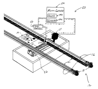
Fig. 1 is a partial isometric view of an apparatus for processing printed
circuit boards
-4-
CA 02375664 2001-11-29
WO 00/73009 PCT/US00/40028
having principles of the present invention;
Fig. 2 is a partial cross-sectional view of the apparatus for processing
printed circuit
boards shown in Fig. 1; and
Fig. 3 is a flow chart showing method steps executable on the apparatus for
processing printed circuit boards shown in Fig. 1.
DETAILED DESCRIPTION OF THE PREFERRED EMBODIMENTS
The present invention provides an apparatus and method for processing printed
circuit
boards including a system for measuring and controlling a solder wave height
generated by a
1 o solder bath which is applied to the printed circuit board during
processing.
Referring to Fig. 1, in one embodiment of the present invention, an apparatus
for
processing printed circuit boards 10 which includes a svstem 50 for measuring
and
controlling solder wave height comprises conveyor system 12 for transporting
printed circuit
board 14 through a number of processing stations. Conveyor system 12 typically
includes a
pair of elongated longitudinal conveyor rails 16 oriented parallel with
respect to each other.
Conveyor rails 16 each have a number of pulleys 18 mounted thereon, whereby at
least one of
the pulleys 18 is motorized by, for example, one or more electric motors (not
shown). Drive
belts 20 are mounted on the pulleys 18 associated with each rail 16 so that
when rotational
motion is transposed to the pulleys 18 by the motor, drive belts 20 move
linearly.
Referring further to Fig. 2. the apparatus for processing printed circuit
boards 10
further includes a plurality of pairs of printed circuit board grippal:g
fingers 22 which are each
mounted on opposing belts so that each pair of gripping fingers 22 face each
other. The
gripping fingers 22 are adapted to securely grip the opposing edge regions of
printed circuit
board 14 for transporting the printed circuit board 14 through a number of
processing stages
including the wave soldering process. In the wave soldering process, the
printed circuit board
14 is moved through a solder wave 24 generated by a solder bath 26 so that a
bottom portion
of the printed circuit board 14 skims the top surface of the solder wave 24. A
capillary effect
enables a predetermined portion of the bottom surface of the board 14 to
receive and retain
the solder.
The system 50 for measuring and controlling the solder wave 24 height includes
a
sensor 52 which is mounted in close proximity to the surface of the solder
wave 24. The
sensor 52 is coupled to a micro-controller 54, via sensor electronics 56. and
the micro-
-5-
CA 02375664 2001-11-29
WO 00/73009 PCT/US00/40028
controller 54 is coupled to a pump motor 58. The pump motor 58 is coupled to
the solder
bath 26 which generates the solder wave 24 and is controlled to operate at a
predetermined
revolution-per-minute ("r.p.m.") to maintain a predetermined solder wave 24
height during
the process of wave soldering printed circuit boards 14.
In an embodiment, the sensor 52 is defined as an eddy current displacement
sensor 52
which can be provided by Micro-Epsilon of Raleigh, North Carolina. The sensor
52 can be
mounted in a preformed aperture (not shown) formed on one of the rails 16,
which positions
the sensor 52 in close proximity to the top surface of the solder wave 24. In
this orientation,
the sensor 52 can communicate with the top surface of the solder wave 24 and
generate an
analog voltage sample representing the distance between the sensor 52 and the
top surface of
the solder wave 24. The analog voltage sample is communicated to the micro-
controller 54,
via sensor electronics 56, and is converted into a predetermined value which
is relative to the
distance between the top surface of the solder wave 24 and the bottom surface
of the printed
circuit board 14. The micro-controller 54 includes a comparator 54a which
receives the value
and compares the value to a predetermined set point.
If the compared value is greater than the set point and exceeds a
predetermined
tolerance range, which indicates that the solder wave 24 height is too high
with respect to the
bottom surface of the printed circuit board 14, then the micro-controller 54
controls the pump
motor 58 to decrease the r.pm.s or speed thereof. Reducing the speed of the
pump motor 58
will proportionately reduce the solder wave 24 height relative to the bottom
surface of the
printed circuit board 14. If the compared value is less than the set point and
is below a
predetermined tolerance range, which indicates that the solder wave 24 height
is too low with
respect to the bottom surface of the printed circuit board 14, the micro-
controller 54 controls
the pump motor 58 to increase the speed of the pump motor 58. Increasing the
speed of the
pump motor 58 will proportionately increase the solder wave 24 height relative
to the bottom
surface of the printed circuit board 14.
In an embodiment, the micro-controller 54 further includes a register 54b,
such as a
linear-shift-register ("LSR") 54b. The LSR 54b is adapted to receive a
plurality of values
from the micro-controller 54. The values represent a plurality of sampled
distances which are
each relative to a distance defined between the top surface of the solder wave
24 and the
bottom surface of the printed circuit board 14. As updated values are provided
to the LSR
54b, older values are discarded, which enables the LSR 54b to maintain
relatively recent
-6-
CA 02375664 2001-11-29
WO 00/73009 PCTIUSOO/40028
values. The values contained in the LSR 54b can be averaged to provide an
average distance
defined between the top surface of the solder wave 24 and the bottom surface
of the printed
circuit board 14. The comparator 54a receives the average value and compares
the average
value to the predetermined set point to determine whether the solder wave 24
height is too
high or to low and to respectively decreases or increases the pump motor 58
similarly to that
previously described.
In an embodiment, the LSR 54b can be averaged when the number of values
contained therein reaches a predetermined LSR-threshold value. For example,
when the
apparatus for processing printed circuit boards 10 commences and the pump
motor 58 is
initially turned on, the solder wave 24 height can greatly fluctuate.
Therefore, the LSR-
threshold value can be set relatively low, e.g. at 15-values. A relatively low
LSR-threshold
value, such as 15-values, will cause the LSR 54b to be averaged after 15-
values have been
received from the n-1icro-controller 54. In this respect, a relatively short
duration will pass
before the pump motor 58 speed will be corrected as a result of the solder
wave 24 height
being too high or too low. Thus, during initial start-up of the apparatus for
processing printed
circuit boards 10, the pump motor 58 speed and associated wave solder 24
height can be
rapidly adjusted to maintain the wave solder 24 height within a predetermined
tolerance range
of a predetermined set point.
On the other hand, after the apparatus for processing printed circuit boards
10,
including the pump motor 58 and associated wave solder 24 height have settled
to an
operational status, the LSR-threshold value can be set relatively high, e.g.
at 100-value.
Setting the LSR-threshold relatively high, such as a 100-value, will cause the
LSR to be
averaged after 100-values have been received from the micro-controller 54. In
this respect, a
relatively long duration will pass before the pump motor 58 speed will be
corrected as a result
of the solder wave 24 being too high or too low. Increasing the LSR-threshold
value also
increases the accuracy of the average value derived therefrom. Therefore, in
increasing the
LSR-threshold, the pump motor 58 speed and associated solder wave 24 height
can be slowly
and accurately adjusted or fine-tuned to maintain the solder wave 24 height
with
predetermined tolerances of the predetermined set point.
Referring to Fig. 3, a method 100 of using the apparatus for processing
printed circuit
boards 10 including a system 50 for measuring and controlling the solder wave
24 height
comprises the steps of a user, at step 110 turning on the apparatus and
pausing momentarily
-7-
CA 02375664 2001-11-29
WO 00/73009 PCT/US00/40028
for the pump motor 58 to form the solder wave 24 to enable the printed circuit
14 wave
soldering process to commence. At step 120, the user can adjust the LSR-
threshold value to a
relatively low value during initial process start-up to increase the number of
times the pump
motor 58 speed will be adjusted for enabling the solder wave 24 height to be
rapidly adjusted.
After the apparatus reaches operational status, the user can adjust the LSR-
threshold value to
a relatively high value to decrease the number of times the pump motor 58
speed will be
adjusted for enabling the solder wave 24 height to be slowly adjusted or fine-
tuned.
At step 130, the sensor can provide analog voltage samples to the micro-
controller 54,
which can be converted to a plurality of values at step 140. The values are
provided to the
LSR 54b, at step 150, and an average value is determined at step 160. The
average value is
compared with a predetermined set point, at step 170, to determine if the
average value is
within a predetermined tolerance range of the set point. If the average value
is within the
predetermined tolerance range of the set point at step 180, then the above
process of
providing values to the LSR 54b, determining an average value and comparing
the average
value with the set point is repeated. If the average value is determined not
within the
predetermined tolerance range of the set point at step 180, a determination is
made as to
whether the average value is too high or too low, at step 190. If the average
value is too high,
which indicates that the solder wave is too high, the speed of the pump motor
58 is decreased,
at step 200, to reduce the solder wave 24 height. Converselv, if the average
value is too low,
which indicates that the solder wave 24 height is too low, the speed of the
pump motor 58 is
increased, at step 210, to increase the solder wave 24 height. The above
process steps can be
cyclically repeated while the apparatus for processing printed circuit boards
is in operation.
What is claimed is:
-8-