Note: Descriptions are shown in the official language in which they were submitted.
CA 02375672 2001-11-30
WO 00/75926 PCTIUSOO/15084
DISK DRIVE CONTROLLER CIRCUIT AND METHOD FOR
SKIPPING DEFECTIVE AND/OR UNDESIRED SECTORS
Background of the Invention
Field of the Invention
The present invention relates generally to computer system mass storage
devices. Specifically, the present
invention relates to a disk drive controller circuit and method for checking
and managing defective andlor undesired sectors
on a disk.
Brief Description of the Related Art
Computer systems often include a host system and one or more peripheral
storage devices that store andlor
provide access to data. One type of peripheral storage device is a hard disk
drive. A hard disk drive typically comprises at
least one platter (collectively "the disk"), which is rotated by a motor, an
actuator that moves a transducer to various
locations over the disk, a microprocessor, a disk drive controller
("controller") and various other electrical circuitry. The
controller is typically an integrated circuit which is mounted to a printed
circuit board within the disk drive. The
microprocessor can be physically embedded within or external to the controller
integrated circuit.
The controller (under the control of the microprocessor) commonly controls
most of the operations of the disk
drive, including handling data from the host computer ("host system" or simply
"host") to be stored on a disk during a write
operation and passing data back to a requesting host computer during a read
operation. The controller is used to retrieve
and send data to and from the disk surface. The controller commonly encodes
the data so that it can be successfully
transferred to and from the disk.
The disk often includes a set of rotating platters which store data. Data can
be written to the disk or read from
the disk any number of times, and the data remains intact after the disk drive
is turned off. A platter may have two
writable surfaces. Each writable surface stores data on concentric rings
called tracks. The number of tracks may vary
from disk to disk. The tracks are divided radially into sectors, which are the
smallest writablelreadable unit of a track. The
number of sectors may vary per track and may vary from disk to disk because
disk manufacturers may have different disk
configurations. There may be 200 or more sectors per track. Each sector
includes data, information about the sector, and
synchronization information.
There are two general types of defects which can occur on a disk platter:
manufacturing defects and grown
defects. Manufacturing defects are defects that occur and are detected during
manufacture. When disks are formatted at
the factory during manufacture, a factory algorithm determines which sectors
are initially defective and creates a list of
sector addresses of all detected manufacturing defects. The procedure of
recording manufacturing defects may be
different from disk to disk and may be unique to each disk manufacturer. The
factory algorithm stores the list of
manufacturing defect addresses on the disk of the disk drive as either
physical addresses or logical block addresses,
depending on the manufacturer's defined implementation of its disk drive. The
disk drive uses the list to perform 'slipping,'
which means for every sector with a manufacturing defect, the address (either
physical or logical, depending on the
1
CA 02375672 2001-11-30
WO 00/75926 PCT/US00/15084
manufacturer's defined implementation) of the next sector to be read or
written is logically incremented from the address
of the last good sector. Thus, during disk drive operation, the disk drive
does not read or write a sector with a
manufacturing defect because the address of that sector has been incremented
to the next good sector.
The other general type of defects are called grown defects, which occur and/or
are detected after manufacture.
Grown defects include sectors which the disk drive determines to be unreadable
or unusable, such as during a format
operation. Grown defects are detected and recorded typically when a sector is
read, but the process may differ depending
on the manufacturer's defined implementation. The data from each sector with a
grown defect is re-assigned to a non-
defective sector.
As with manufacturing defects, the locations of grown defects and their re-
assigned sector addresses are
typically stored on the disk as either physical or logical addresses,
depending on the manufacturer's defined
implementation. The grown defect locations may be transferred from the disk to
a random access memory (RAM) each
time the disk drive is powered on.
Some disk drive controllers include one or more registers which are used to
temporarily store the addresses of
defective sectors to be skipped or re-assigned during a current read or write
operation.
Summary of the Invention
One drawback with some disk drive controllers is the limited number of
registers in the disk drive controller which
are assigned to identify defective sectors on a track to be skipped or re-
assigned during a read or write operation. The
number of registers restricts the total number of defective sectors that can
be skipped or re-assigned during a read or write
operation. In some disk drives, the number of defects on a particular track
may be greater than the number of available
registers used to identify defects on a track. Adding more registers would
require adding more gates, which increases the
cost of manufacturing the disk drive controller.
In addition to manufacturing costs, another drawback to adding more registers
is trying to guess in advance how
many registers are sufficient to handle all the defects of a particular track
of a particular disk platter. Different disk
platters may have a different number of sectors per track and a different
number of tracks. Moreover, as disk technology
improves, the number of sectors per track may increase, which may lead to more
defective sectors to be managed,
skipped, andlor re-assigned by the disk drive controller.
One solution is to partition the defect management operation into multiple
parts because the controller can only
skip a certain number of defective sectors for a given read or write operation
(based on the limited number of registers). If
each part of a multi-part defect management operation skipped or re-assigned a
particular number of defective sectors,
then there may be enough registers to handle most or all of the defects on a
particular track. But splitting the defect
management operation into multiple parts increases the time of the overall
defect management operation and degrades disk
drive performance. An important goal in current disk drives is to minimize the
amount of time for read and write
operations.
The present invention relates to a disk drive controller circuit and method
for keeping track of defective andlor
undesired sectors on a disk and skipping such defective or undesired sectors
during read or write operations. The present
2
CA 02375672 2001-11-30
WO 00/75926 PCT/USOO/15084
invention recognizes and takes advantage of the fact that defective sectors
tend to be in close proximity with each other
and are often found together in groups of contiguous or consecutive sectors.
The disk drive controller of the present
invention uses 'skip range check registers' or 'skip check registers' which
can store the locations of ranges of consecutive
defective sectors.
By storing the defective sector information within the controller as ranges of
defective sectors, the present
invention may reduce the quantity of registers andlor register logic needed to
keep track of defects. Alternatively, the
present invention may increase (over prior designs) the number of defective
sectors that can be handled during a read or
write operation without a substantial increase in register logic.
Furthermore, because the disk drive is configured to read or write data on a
track continuously sector-by-sector,
the skip range check registers allow the controller to quickly skip the
defective sectors in groups instead of single units.
Thus, the disk drive controller circuit and method of the present invention
reduces the problems of adding more registers,
trying to guess how many more registers are needed, and partitioning the
defect management operation into multiple parts.
Various disk drive manufacturers may use various defect management schemes.
Any one of a variety of known
defect management schemes may be used with the present invention.
One embodiment also allows the host system to skip or mask certain undesired
sectors during a read or write
operation. These sectors are not defective, but they are undesired by the host
system during a particular read or write
operation.
One aspect of the present invention relates to a disk drive controller in a
disk drive configured to read and
write data to one or more sectors on one or more tracks of a disk as requested
by a host system. The disk drive
controller comprises at least one register configured to store (a) a sector
address of a first sector to be skipped during
a read or write operation; and (b) a range value which indicates a number of
consecutive sectors to be skipped during
the read or write operation. The disk drive controller further comprises a
control circuit configured to use the sector
address and the range value to skip a range of consecutive sectors during the
read or write operation. In one
configuration, the control circuit comprises a state machine. One
configuration of the register further comprises a re-
assign bit which indicates that a particular sector or range of consecutive
sectors have been re-assigned and should be
skipped. Another configuration of the register further comprises an increment
logical block address (LBA) bit which allows
the host system to direct the controller to skip certain undesired (but not
defective) sectors during a read or write
operation.
Another aspect of the present invention relates to a method of skipping one or
more sectors on a disk of a
disk drive during a read or write operation requested by a host system. The
method comprises generating a list of
sectors to be skipped during the read or write operation; identifying within
the list at least one range of consecutive
sectors to be skipped; converting the range into an address and a range value
to generate a compressed list; and
loading the compressed list into a set of registers of a disk drive
controller.
3
CA 02375672 2007-11-09
In accordance with an aspect, there is provided a disk drive controller in a
disk drive configured to read
and write data to one or more sectors on one or more tracks of a disk as
requested by a host system, the disk drive
controller comprising at least one register configured to store: a sector
address of a first sector to be skipped
during a read or write operation; a range value which indicates a number of
consecutive sectors to be skipped
during the read or write operation; wherein at least some of the sectors to be
skipped have grown defects, and a re-
assign bit which indicates whether the disk drive controller has re-assigned
data from one or more defective
sectors of the disk to non-defective other sectors on the disk, and the
reassign bit indicates the consecutive
sectors that should be skipped; and a control circuit configured to use the
sector address and the range value to
skip a range of consecutive sectors during the read or write operation.
In accordance with another aspect, there is provided a method of skipping one
or more sectors on a disk
of a disk drive during a read or write operation requested by a host system,
the method comprising generating a
list of sectors to be skipped during a read or write operation using a master
defect list and at least one sector
identified by a host in the read or write operation; identifying within the
generated list at least one range of
consecutive sectors to be skipped; converting the range into an address and a
range value to generate a
compressed list; loading the compressed list into a set of registers of a disk
drive controller; and skipping the
sectors identified with the address and the range value in the compressed list
during the reading from or writing to
the disk.
In accordance with yet another aspect, there is provided a method of skipping
one or more sectors on a
disk of a disk drive during a read or write operation requested by a host
system, the method comprising:
generating a list of sectors to be skipped during a read or write operation
using a master defect list and at least one
sector identified by a host in the read or write operation; identifying within
the generated list at least one range of
consecutive sectors to be skipped; converting the range into an address and a
range value to generate a
compressed list; loading the compressed list into a set of registers of a disk
drive controller; wherein the act of
loading the compressed list into a set of registers of a disk drive controller
comprises loading the registers in
ascending order with no empty registers in between fill registers; and
skipping the sectors identified with the
address and the range value in the compressed list during the reading from or
writing to the disk.
In accordance with yet another aspect, there is provided a method of skipping
one or more sectors on a
disk of a disk drive during a read or write operation requested by a host
system, the method comprising generating
a list of sectors to be skipped during a read or write operation using a
master defect list and at least one sector
identified as a sector that has been re-assigned to a non-defective sector
because of a grown defect; identifying
within the generated list at least one range of consecutive sectors to be
skipped; generating a compressed list by
converting the range into an address and a range value and including a re-
assign bit identifying the at least one
sector; loading the compressed list into a set of registers of a disk drive
controller; and skipping the sectors
identified with the address and the range value in the compressed list during
the reading from or writing to the
disk.
3a
CA 02375672 2007-11-09
In accordance with still yet another aspect, there is provided a disk drive
controller in a disk drive
configured to read and write data to one or more sectors on one or more tracks
of a disk as requested by a host
system, the disk drive controller comprising at least one register configured
to store: a sector address of a first
sector to be skipped during a read or write operation; a range value which
indicates a number of consecutive
sectors to be skipped during the read or write operation; wherein at least
some of the sectors to be skipped are
explicitly designated by the host system during the read or write operation
and the range of values is loaded as a
compressed list in ascending order; and a control circuit configured to use
the sector address and the range value
to skip a range of consecutive sectors during the read or write operation.
3b
CA 02375672 2001-11-30
WO 00/75926 PCT/USOO/15084
Brief Description of the Drawings
Figure 1 illustrates a host system and a disk drive according to one
embodiment of the invention and illustrates a
host system connected to the disk drive.
Figure 2A illustrates an example of a track on a disk and two skip registers.
Figure 2B illustrates an example of a track on a disk and one configuration of
a skip range check register in the
disk drive of Figure 1.
Figure 3 illustrates one configuration of a set of skip range check registers
in the disk drive of Figure 1.
Figure 4 illustrates one configuration of a bit map used by the disk drive of
Figure 1.
Figure 5 illustrates one configuration of a state machine method performed by
the disk drive of Figure 1.
Figure 6 illustrates an example of a track on a disk and a set of skip range
check registers of Figure 3.
Figure 7 illustrates a one configuration of a firmware method performed by the
disk drive of Figure 1.
Detailed Description of the Preferred Embodiments
A preferred embodiment of the present invention is described herein, which is
intended to illustrate, and not limit,
the scope of the invention.
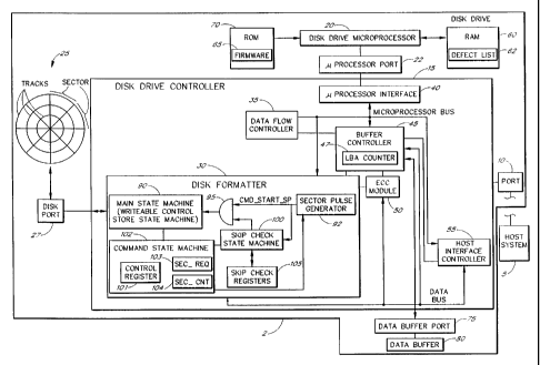
Figure 1 illustrates a disk drive 2 according to one embodiment of the
invention. The disk drive 2 is shown
together with a host system (host) 5, which may, for example, be a personal
computer (PC). The disk drive 2 comprises a
disk drive controller circuit (controller) 15, a host interface port 10, a
disk port 27, a local or disk drive microprocessor
(microprocessor) 20, a microprocessor port 22, a data buffer port 75, a read-
only memory (ROM) 70, a random-access
memory (RAM) 60 and a data buffer 80. The disk drive controller 15 reads and
writes data to a disk 25.
The host interface port 10 may, for example, be a Small Computer Standard
Interface (SCSI) port, an Advanced
Technology Attachment (ATA) bus port, or a Fibre Channel port. The
microprocessor 20 is preferably a general purpose
microcontroller, and may be either physically embedded within the controller
15 or external to the controller 15. The data
buffer 80 may be either inside or outside the controller 15. The ROM 70 stores
an executable firmware 65, which may be
copied to the RAM 60 at boot-up and executed by the microprocessor 20.
Alternatively, the ROM 70 may store a set of
instructions to download firmware from the disk 25 to the RAM 60.
The RAM 60 stores a defect list 62 which is loaded from the disk 25 or any
other suitable location by the
firmware 65 at boot-up. The defect list 62 may be a master list of all
manufacturing and grown defects for the entire disk
25. Alternatively, in another configuration, the defect list 62 may be loaded
into RAM 60 by the firmware 65 at the
beginning of each read or write operation. In this configuration, the defect
list 62 may be a portion of the master list of all
manufacturing and grown defects for the entire disk 25. In this configuration,
the firmware 65 may load a part of the
master list on a track-by-track basis or a zone-by-zone basis (depending on
the manufacturer's defined implementation) as
needed by a read or write command.
In the illustrated embodiment of Figure 1, the disk drive controller 15
comprises a microprocessor interface 40, a
data flow controller 35, a buffer controller 45, an error correction code
(ECC) module 50, a disk formatter 30 and a host
interface controller 55. The host interface controller 55 may comprise a SCSI
controller or SCSI processor, an ATA
4
CA 02375672 2001-11-30
WO 00/75926 PCT/USOO/15084
processor or a Fibre Channel interface manager. The buffer controller 45
includes at least one logical block address (LBA)
counter 47, which counts the logical block addresses of the sectors associated
with a read or write operation.
The disk formatter 30 comprises a main state machine 90, a sector pulse
generator 92, an AND logical function
gate 95, a command state machine 102, a skip check state machine 100 and a set
of skip check registers 105. The disk
formatter registers comprise a disk formatter control register 101, a SEC_REQ
register 103 and a SEC_CNT register 104.
Alternatively, in other configurations, other circuit architectures may be
used to implement the disclosed functions.
General Operation Controller and Microprocessor
The general operation of the disk drive controller 14 and microprocessor 20 is
described with reference to
Figures 1 and 7. Figure 7 illustrates one configuration of a firmware method
performed by the disk drive 2 of Figure 1. In a
process block 700 of Figure 7, the disk drive 2 receives and processes a read
or write command from the host system 5.
Specifically, the host 5 initiates a disk drive operation by sending a read or
write command to the host interface controller
55 of the disk drive controller 15. The microprocessor 20 reads the read or
write command from the host interface
controller 55. The read or write command starts at a selected logical block
address and may involve more than one track.
In a process block 702, the microprocessor 20 executes firmware 65 which
identifies the track(s) to be read or
written. The firmware 65 converts or translates the logical block addresses of
the read or write command into specific
physical sector locations (addresses) to be read or written an the disk 25.
The translation is defined by a manufacturer's
implementation of its disk drive.
In a process block 704, the firmware 65 generates a list of sectors to be
skipped within the identified track(s) of
the read or write operation. To generate this list, the firmware 65 may use a
bit map, if any (such as the one illustrated in
Figure 4), associated with the read or write command and the defect list 62
from the disk 25. As described above, the
defect list 62 used by the firmware 65 may be a master list of all manufacture
and grown defects on the disk 25 or a
portion of the master list.
In a process block 706, the firmware 65 converts the list 62 of sectors to be
skipped into an appropriate format
for loading the skip range check registers 105. This includes, for example,
combining consecutive defective sector
addresses into a starting address and a range (or length) of consecutive
defective sector addresses. Thus, the defect list
62 is converted to a condensed or compressed list. The firmware 65 also uses
the defect list 62 to generate a re-assign bit
(to be loaded into the re-assign bit 162 of the skip check register set 170)
for sectors, specified by the read or write
command, with grown defects.
In a process block 708, the firmware 65 loads all of the required control
parameters to perform the command
into the appropriate registers of the controller 15, such as the disk
formatter control register 101, the SEC_REQ register
103, the SEC CNT register 104 and the skip check registers 105. For the skip
check register configuration of Figure 3,
the firmware 65 loads the four fields 162-168 as required.
One of the purposes of the control parameters is to specify which physical
sectors and which tracks will be
written to or read. The SEC REQ register 103 initially contains the start or
first sector address (address of the lowest
physical sector address) identified for executing a read or write command from
the host system 5. The SEC_CNT register
5
CA 02375672 2001-11-30
WO 00/75926 PCT/USOO/15084
105 initially specifies the total number of sectors identified by the read or
write command, and during the course of the
operation, specifies the number of remaining sectors to be processed.
After the registers 101, 103, 104 and 105 are loaded, the firmware 65 issues a
read/write command to the disk
formatter 30, as shown in a process block 710. The disk formatter 30
preferably executes the command automatically
with no further intervention by the microprocessor 20. The sector pulse
generator 92 generates a start command sector
pulse (CMD_START_SP) to the AND logical function gate 95. The CMD_START_SP
identifies the first specified sector
ID, SEC REQ. The sector pulse generator 92 also sends the CMD START SP to the
skip check state machine 100.
The skip check state machine 100 determines whether the value stored in the
SEC_REQ register 103 refers to a
sector to be skipped. The skip check state machine 100 generates an output
which is input into the AND gate 95, along
with the CMD_START SP from the sector pulse generator 92. If the output of the
skip check state machine 100 is 'low,'
then the sector is skipped. If the output of the skip check state machine 100
is 'high,' then the sector is not skipped. The
output of the AND gate 95 is input into the main state machine 90.
The skip check state machine 100 checks for defective sectors using the
contents of the skip check registers
105. The skip check state machine 100 stops the operation if it detects an
address to a sector that is designated as a
sector to be re-assigned because of a grown defect. The firmware 65 then uses
a re-assign algorithm to re-assign the data
to a sector without grown defects (e.g., for a write operation) or to identify
a replacement sector (e.g., for a read
operation).
When the command is complete, the disk formatter 30 sends an interrupt to the
microprocessor 20 andlor sets a
flag. The interrupt may indicate that the command is complete, and the disk
formatter 30 is ready to execute another
command.
Read or Write
In one configuration, if the command from the host 5 is a read command, the
requested data is read from the disk
into the data buffer 80. When a certain amount of data is in the buffer 80,
the microprocessor 20 causes the controller
15 to send the data from the buffer 80 to the host 5. If the command from the
host 5 is a write command, the disk
25 formatter 30 and the ECC module 50 encode the data before it is stored on
the disk 25.
Firmware Functions
The firmware 65 is preferably configured to execute three primary functions
that relate to the defect
management scheme. At boot-up, the firmware 65, when executed by the
microprocessor 20, causes the disk drive
controller 15 to read the list of sectors with manufacturing defects from the
disk 25 and stores this list in the RAM 60, a
data buffer or some other area (unknown to the disk controller). The list may
relate to a zone, a platter or some other unit
designated by the disk drive manufacturer. During a read or write operation,
the firmware 65 transfers a part of this list to
the disk formatter 30. The transferred part of the list covers the particular
track(s) which is related to the sectors
specified by the host system 5. The disk formatter 30 skips over certain
sectors of the track(s) according to the
transferred partial list. This is part of the defect management operation
described above.
6
CA 02375672 2001-11-30
WO 00/75926 PCT/US00/15084
The firmware 65 also re-assigns sectors with grown defects. The re-assign
procedure may vary depending on the
disk drive manufacture's implementation. When an error is encountered, such as
during a read operation, the firmware 65
attempts to recover the data and re-assign the data to an alternate 'good'
sector that is not defective. The good sector
may be located anywhere on the disk 25. The firmware 65 controls and maintains
a record of sector re-assignments. At
the beginning of a subsequent read or write operation (after the data has been
re-assigned), the firmware 65 programs the
location of one or more defective sectors to be skipped into the skip check
registers 105 within the disk drive formatter
30. Re-assigned sectors cause the firmware 65 (and the disk formatter 30) to
read or write up to the re-assign address,
determine the address of the re-assigned sector, read or write this sector,
and then return to the remaining sectors of the
read or write command.
Before a read or write operation, the firmware 65 may also program the disk
formatter 30 to skip certain sectors
which are undesired by the read or write command from the host 5. Undesired
sectors are not defective (they contain
valid, readable data), but they are not identified by the host system 5 to be
transferred for various reasons. For example,
certain sectors may not be used in a specialized command set, such as 'skip
mask read' and 'skip mask write' used in
redundant array of inexpensive disk (RAID) controllers. The SCSI protocol, for
example, has specialized commands which
may be used to exclude certain undesired sectors or a range of sectors.
The firmware 65 preferably reprograms the registers 101, 103, 104 and the skip
registers 105 before each new
read or write operation because the control parameters may be different for
each read or write operation.
Overview of Defect Management Operation -- Main St Mach. and Skip St Mach.
Function
One part of the defect management operation is described with reference to
Figure 1. After the first sector is
checked, the main state machine 90 of the disk formatter 30 preferably
operates in parallel with the skip check state
machine 100. The skip check state machine 100 performs a skip check procedure
on subsequent identified sectors while
the main state machine 90 performs other processing functions.
SEC REQ and SEC CNT
The skip check state machine 100 checks the skip registers 105 to determine
whether the sector address of a
requested sector (SEC_REQ) is designated as a skip sector by the firmware 65.
The SEC_REQ register 103 preferably
acts as a counter, which is incremented by 1 after each requested sector
address (requested by the read or write
operation) is checked against the skip sector addresses (designated as a skip
sector by the firmware 65) stored in the skip
registers 105.
If the requested sector (SEC_REQ) is designated as a skip sector, the skip
check state machine 100 skips that
sector and checks the next sequential sector (SEC_REQ + 1) on the track. If
the sector is not designated as a skip sector,
the skip check state machine 100 allows the main state machine 90 to process
the sector, and the main state machine 90
reads or writes data to or from the sector. The main state machine 90
decrements the total number of requested sectors
(SEC CNT) by 1 after each sector is successfully found and read or written.
When SEC_CNT is decremented to zero, the
read or write operation is complete.
7
CA 02375672 2001-11-30
WO 00/75926 PCT/US00/15084
Existing Skip Register Confinuration
Figure 2A illustrates an example of a track 120 on the disk 25, a first skip
register 125 and a second skip
register 127, and will be used to illustrate a deficiency in existing designs.
Only 6 sectors 130-140 and two skip registers
125, 127 are shown for purposes of this example. But a track may comprise 200
or more sectors, and a disk formatter 30
may have several skip registers.
In Figure 2A, each skip register 125, 127 can store or map the location (also
called a sector address or a sector
ID) of a single defective sector. But the number of defective sectors on a
track to be read or written may be greater than
the number of skip registers. For example, as shown in Figure 2A, there are
three defective sectors 132-136 and only 2
skip registers 125, 127. In one existing method, the disk formatter 30
partitions a read or write operation intended for the
track 120 into at least two operations because its defect management operation
can only handle a limited number of
sectors to be skipped, which is two in this example. A first defect management
operation would use the first skip register
125 to store the location of the first sector defect 132 and use the second
skip register 127 to store the location of the
second sector defect 134. A second defect management operation would use the
first skip register 125 to store the
location of the third sector defect 136. A first read operation would read up
to sector n 130, and a second read operation
would read from n + 1 to any other sectors further along the track 120.
One disadvantage of partitioning the defect management operation is that is
increases the time needed to
complete the read or write operation, and thereby reduces disk drive
performance.
Skip Range Check Register
Figure 2B illustrates a disk track 120 and one configuration of a skip range
check register 150 in accordance
with one embodiment of the present invention. In Figure 2B, the skip range
register 150 comprises a skip sector location
or ID field 154 (SKIP ID) and a length field 152 (LENGTH). The skip sector ID
field 154 specifies the sector location of a
first sector to be skipped on the track 120, such as the first defective
sector 132 shown in Figure 2B. In a preferred
configuration, this skip sector ID is a physical address, not a logical
address.
The LENGTH field 152 specifies the number of consecutive defective sectors
which should be skipped, starting
with the first defective sector 132. A LENGTH of '1' indicates that only the
sector at the SKIP ID address is to be
skipped. A LENGTH of '2' indicates that the two sectors at the SKIP ID and the
SKIP ID + 1 addresses are to be
skipped. For example, for the track 120 shown in Figure 28, the LENGTH field
152 is three. The LENGTH field 152 allows
the disk formatter 30 to skip more than one sector while it consumes only one
skip register 150.
The skip range check register 150 takes advantage of the fact that defective
sectors are often found together in
groups of contiguous or consecutive sectors. A disk formatter 30 (Figure 1)
with a single skip range check register 150
(Figure 2B) can perform a read or write operation on the track 120 (with the
defects shown) with a single defect
management operation, instead of partitioning the operation into multiple
parts. This reduces the time of a read or write
operation and improves disk drive performance.
Figure 3 illustrates one configuration of a set 170 of skip range check
registers 180-210. Each register 180-210
may represent a bad sector or range of consecutive bad sectors. The skip range
check registers 180-210 of Figure 3
8
CA 02375672 2001-11-30
WO 00/75926 PCT/USOO/15084
comprise a 10-bit SKIP_ID field 168, a 4-bit LENGTH field 166, an INCREMENT
LBA bit 164 and a RE-ASSIGN bit 162.
The SKIP ID 168 specifies the location of a first sector to be skipped or re-
assigned on the track 120. The LENGTH field
166 specifies the number of consecutive sectors to be skipped or re-assigned.
A value of '0' in the LENGTH field 166
indicates that the skip range check register 160 contains an entry that is not
valid. In other words, if LENGTH = 0, then
no skip is required.
The entries within the skip registers 180-210 are preferably loaded by the
firmware 65 in ascending order. The
location of the lowest physical sector or range of sectors to be skipped is
loaded in the first skip register 180. The location
of the second-lowest physical sector or range of sectors to be skipped is
loaded in the second skip register 182, and so on.
In this preferred configuration, there are no empty registers in between full
registers. Thus, once an empty register is
encountered by the skip check state machine 100, no further skip check
registers need to be read. The advantages of
loading the entries in ascending order with no empty registers in between full
registers is explained below with reference to
Figures 5 and 6.
Although 16 skip registers 180-210 are shown in Figure 3, other embodiments of
the present invention may have
more or less than 16 skip registers. The skip check registers 105 in Figure 1
preferably comprise the set 170 of skip range
check registers 180-210 of Figure 3. Alternatively, in other embodiments, the
skip range check entries may be
implemented with a first-in-first-out (FIFO) module or stack stored in a
memory instead of registers 180-210.
Logical Block Addresses
The INCREMENT LBA bit 164 allows a read or write operation from the host
system 5 to skip certain undesired
sectors which are not defective. In general, the host system 5 perceives data
as stored in a continuous sequence of logical
block addresses (LBAs). The disk controller 15 controls the arrangement of how
data is stored on the disk 25, and the
firmware 65 controls the translation between LBAs and physical sector
addresses. The mapping of LBAs to physical
addresses preferably takes place transparently to the host system 5. Thus,
logical block addresses may not match
physical sector IDs on the disk.
For example, logical block addresses 1-19 used by the host 5 may be stored on
sectors 8-26 of a first track of a
first disk platter (not shown), LBA 20-22 may be stored on sectors 1, 5 and 6
of a second track of the first disk platter (as
in Figure 2B), and LBA 23-30 may be stored on sectors 1-8 of a track of a
second disk platter. Furthermore, data sectors
may be re-assigned to various physical sector IDs, but the logical block
addresses still remain sequential.
The LBA counter 47 (Figure 1) tracks the logical block addresses of the data
sectors stored on the disk 25.
When the disk controller 15 writes data to the disk 25, the LBA counter 47 is
automatically incremented, and an assigned
LBA value is inserted with the data as it is stored on a sector of the disk
25. There is no LBA value associated with
skipped, defective sectors which were detected during manufacturing. The disk
formatter 30 may automatically check the
LBA value of each sector as it is read from the disk 25.
Increment LBA Bit
Figure 4 illustrates one configuration of a list or bit map 180 which may be
generated by the host system 5
(Figure 1) in association with a read or write command from the host 5. The
bit map 180 is stored in the RAM 60 when
9
CA 02375672 2001-11-30
WO 00/75926 PCTIUSOO/15084
the disk drive 2 receives the bit map 180 from the host system 5.
Alternatively, other means of informing the disk drive
controller 15 to skip certain undesired sectors may be used instead of or in
addition to the bit map 180 of Figure 4.
In operation, the firmware 65 uses the bit map 180 to determine which logical
block addresses are desired and
which logical block addresses are not desired by the host system 5 in a
particular read or write operation. Each bit 182-
204 in the bit map 180 represents a logical block address which is associated
with a physical sector address of a sector on
a track. A '1' indicates a logical block address desired by the host 5 in a
particular read or write command. A '0' indicates
an undesired logical block address and a sector to be skipped by the disk
controller 15. The firmware 65 uses the bit map
180 of Figure 4 and the increment LBA bit 164 (Figure 3) to coordinate the LBA
counter 47 with sectors which are
undesired by a particular read or write operation. Specifically, the firmware
65 uses the bit map 180 to configure entries
in the skip check registers 105 (Figure 1).
For example, in Figure 4, the first three bits 182-186 are '1s' and the next
two bits 188-190 are 'Os.' This
indicates that logical block addresses 1-3 will be used in a read or write
operation, and logical block addresses 4-5 will not
be used (undesired). The firmware 65 (Figure 1) converts the bit map 180 to an
entry for a skip range check register 180-
210 (Figure 3) to skip sectors associated with the logical block addresses 4-
5. The firmware 65 sets the increment LBA
bit 164 of the skip check register entry to a predefined state, such as '1,'
and loads the length (range) field 166 (Figure 3)
with the value '2.' This indicates that the LBA counter 47 will be incremented
by 2 for the two sectors skipped.
Thus, the increment LBA bit 164 indicates whether or not the LBA counter 47
should be incremented. The
undesired (but not defective) sectors are skipped (not read or written), and
the increment LBA bit 164 causes the LBA
counter 47 to count the skipped sectors as if they had been valid and read or
written. The ability to mark certain sectors
undesired by a particular read or write operation adds more flexibility to the
disk controller 15 and the skip check method,
but is not essential.
Re-assign Bit
As described above, the re-assign bit 162 of Figure 3 is loaded by the
firmware 65 along with the rest of the
fields 164-168. When the re-assign bit 162 is set to 1, this indicates that
all sectors specified by the skip sector ID field
168 and the length field 166 have been re-assigned and should be skipped. In
other words, all sectors in the range from
SKIP ID to SKIP ID +(LENGTH - 1) are to be skipped. Skipped sectors are not
counted as part of the sector count
(SEC CNT).
Access to Skip Registers
Access by the microprocessor 20 to the set 170 of skip range check registers
190-210 is through a FIFO-Iike
interface (not shown) which occupies a two-byte address space. Before the
firmware 65 loads the skip check registers
180-210 for a read or write operation, the disk formatter 30 preferably
initializes the FIFO interface by setting a 'skip FIFO
initialize' bit in the disk formatter control register 101 of Figure 1.
Setting the skip FIFO initialize bit causes all the fields of
each skip check register 190-210 to be reset to 0, including the length fields
and the re-assign bits.
10
CA 02375672 2001-11-30
WO 00/75926 PCT/US00/15084
Address Logic and Pointer
The disk formatter 30 further comprises skip register address logic, such as a
skip register address pointer PNTR
172, which points to a selected skip check register 180-210 as shown in Figure
3. A load pointer variable is used by the
firmware 65 ta load the registers 180-210. A read pointer variable is used by
the skip check state machine 100 to read
the registers 180-210 after the registers 180-210 are loaded by the firmware
65.
At the beginning of a read or write operation, the disk formatter 30 resets
the pointer PNTR 172 (load pointer
variable) to '0.' When the firmware 65 (executed by the microprocessor 20)
loads the skip check registers 180-210, the
firmware 65 accesses and writes to a single address designated by the pointer
172 (load pointer variable). The disk
formatter 30 automatically increments the PNTR 172 (load pointer variable)
such that the skip check registers 180-210 in
the set 170 are incrementally loaded. In one configuration, if there are more
than 16 entries (more than the total number
of implemented registers 190-210) written by the firmware 65 to the registers
180-210, then the pointer 172 (load pointer
variable) wraps around the last register 210 and continues to increment
through successive registers 180-210. The wrap-
around nature of the pointer 172 (load pointer variable) causes the disk
formatter 30 to over-write previous data in the
registers 180-210.
When the pointer 172 is used by the skip check state machine 100, the pointer
172 (read pointer variable) will
wrap-around the skip check range registers 180-210, but the skip check state
machine 100 stops once it starts to wrap
and causes the controller 15 to process the SEC_REQ.
Skip Check State Machine - Figures 5 and 6
Figure 5 illustrates one embodiment of a skip check method performed by the
skip check state machine 100 of
Figure 1. Figure 6 illustrates an example of a track 250 with a plurality of
sectors 252-268 and a set of skip range check
registers 270-276, which are similar in structure to the skip range check
registers 180-210 shown in Figure 3.
The operation of the skip check state machine 100 is described with reference
to Figures 1-6. In Figure 1, the
firmware 65 initializes and starts the main state machine 90 and the command
state machine 102. The command state
machine 102 starts the skip check state machine 100 and may wait for the skip
check state machine 100 to finish. In
Figure 5, the skip check state machine 100 is initially in an idle state 210
waiting for a SKIP START command from the
command state machine 102. When the skip check state machine 100 receives a
SKIP START command, the state
machine 100 proceeds to a SKIP_STATE_1 215. The command state machine 102
transfers the SEC_REQ 103 (ID of the
next requested sector) to the sector pulse generator 92. In SKIP_STATE_1 215,
the skip check state machine 100
receives the first value stored in SEC REQ register 103 of Figure 1 from the
sector pulse generator 92 and compares this
value with the skip sector ID (SKIP ID) of the first skip check register 270.
Initially, the PNTR 298 is on the first skip
check register 270.
Re-assign
In SKIP STATE 1 215, if SEC REQ is equal to the skip sector ID of the first
skip check register 270, and the
re-assign bit 290 is set to 1, then the skip check state machine 100 sets a re-
assign interrupt (as discussed below) and
transfers control back to the command state machine 102 (or the main state
machine 90). The skip check state machine
11
CA 02375672 2001-11-30
WO 00/75926 PCT/US00/15084
100 proceeds from SKIP-STATE-1 215 to the idle state 210. For example, in
Figure 6, if SEC_REQ = 2 and SKIP_ID -
2, then SEC REQ = SKIP ID. If the re-assign bit is set to 1, the disk
formatter 30 may search the track or the disk 30 for
the requested re-assigned data sectors. This search for re-assigned sectors
may be directed by the firmware 65 and is
preferably a separate process from the skip check state machine method as
shown in Figure 5.
In SKIP STATE 1 215, if SEC REQ is less than or equal to (SKIP ID + (LENGTH -
1)), this means that the
SEC REQ is within the range of sectors designated to be skipped by the first
skip check register 270. For example, in
Figure 6, if SEC_REQ = 3, and (SKIP_ID + (LENGTH - 1-) - 2 + (2-1) = 3, then
SEC_REQ falls within the range of
sectors designated to be skipped by the first skip check register 270. If the
re-assign bit 290 is set to 1, then the skip
check state machine 100 suspends its operation (proceeds to the idle state
210), sets a re-assign interrupt and transfers
control back to the command state machine 102 (or the main state machine 90).
The re-assign interrupt informs the firmware 65 (Figure 1) that the data has
been re-assigned to another sector
location. As described above, grown defects are detected and recorded
typically when a sector is read, but the process
may differ depending on the manufacturer's defined implementation. The data
from each sector with a grown defect is re-
assigned to a non-defective sector. In response to the re-assign interrupt,
the firmware 65 determines where the data has
been re-assigned, for example, by using a list of re-assigned sector
addresses. The firmware 65 sends the re-assigned
sector address with a new command to the disk formatter 30 for the re-assigned
sector. The skip check state machine
100 remains in the idle state 210 until another SKIP START command is received
from the command state machine 102.
LENGTH = 0
In SKIP STATE 1 215, if the LENGTH field 294 is equal to '0,' then the skip
check entry is not valid, and no
skip is required. For example, in Figure 6, if the LENGTH fields of all the
registers 270-276 are '0,' then there are no skips
required. The skip check state machine 100 then proceeds to a SKIP STATE_3
225, which indicates that a 'good' sector
has been found by the skip check state machine 100, and the disk formatter 30
may read from or write to the sector, as
described below.
SEC REQ < SKIP ID
In SKIP STATE 1 215, if the LENGTH field is not equal to zero, and SEC REQ is
less than SKIP ID, this means
that the requested sector address is lower than the SKIP_ID of the skip check
register currently designated by the pointer
PNTR 298, which in this case is the first skip register 270. For example, in
Figure 6, if SEC_REQ = 1 and SKIP_ID m 2,
then SEC_REQ < SKIP_ID. If SEC_REQ is less than the SKIP_ID of the first skip
check register 270, then the requested
sector address (SEC REQ) is lower than the SKIP ID of all the skip check
registers 270-276 because of the ascending
order.
This is an advantage of the skip check registers' ascending order because the
skip check state machine 100 does
not need to check the entries of all the skip check registers 270-276. As soon
as the skip check state machine 100 finds a
SEC REQ < SKIP ID condition, the skip check state machine 100 can immediately
return an enable signal to command
state machine 102 andlor the main state machine 90 to read or write the
requested sector SEC REQ. The skip check
state machine 100 proceeds from SKIP-STATE-1 215 to SKIP_STATE_3 225.
12
CA 02375672 2001-11-30
WO 00/75926 PCT/US00/15084
Skip Check Done
In SKIP_STATE_3 225, the skip check state machine 100 proceeds to a SKIP
STATE_4 230, which indicates
that the skip check procedure is done for the sector currently designated by
SEC REQ. The skip check state machine 100
returns control back to the command state machine 102 and/or the main state
machine 90. The disk formatter 30 causes
the disk drive 15 (Figure 1) to read or write the sector designated by SEC_REQ
on the track 250. For example, in Figure 6,
the disk formatter 30 causes the disk drive 15 to read or write to the sector
252 at SEC REQ = 1.
The command state machine 102 decrements the total number of requested sectors
(SEC CNT) in the SEC CNT
register 104 after a sector is successfully found and read. When the SEC CNT
reaches zero, there are no more sectors
associated with that particular read or write operation, and the read or write
operation is complete.
Skip Check Continue
In SKIP STATE_4 230, the skip check state machine 100 waits for a signal from
the command state machine
102 andlor the main state machine 90. If there are more sectors to be read or
written in the read or write operation
(SEC_CNT is not equal to zero), the command state machine 102 causes the
sector pulse generator 92 to send another
sector pulse to the skip check state machine 100. The command state machine
102 sends a SKIP CONT command to the
skip check state machine 100 to continue the skip check process for the next
sector. The skip check state machine 100
proceeds from SKIP STATE 4 230 to a SKIP STATE 5 235. The skip check state
machine 100 increments the sector
requested, SEC_REQ, to point to the next sector on the track and starts the
skip check method again.
For example, if SEC_REQ is 1, then it is incremented to SEC_REQ + 1 = 2. The
skip check state machine 100
then proceeds to SKIP STATE 1 215 and performs the skip check procedure on the
next SEC REQ value, which is
SEC REQ + 1= 2.
The skip check state machine 100 preferably checks the next requested sector
(SEC REQ + 1) to be read or
written while the disk formatter 30 reads the present requested sector
(SEC_REQ). This saves time and improves the
efficiency of a read or write operation.
Increment Pointer
In SKIP_STATE_1 215, if SEC_REQ is greater than (SKIP_ID + (LENGTH - 1)), this
means that the requested
sector address is higher than the SKIP ID of the skip check register currently
designated by the pointer PNTR 298. For
example, in Figure 6, if SEC REQ = 4, SKIP ID = 2, and (LENGTH - 1) = 1, then
(SKIP ID + (LENGTH - 1)) = 1, and
SEC REQ > (SKIPID + (LENGTH - 1)). The skip check state machine 100 proceeds
from SKIP STATE 1 215 to
SKIP_STATE_2 220 shown in Figure 5. The skip check state machine 100
increments the pointer PNTR 298 to point to
the next skip check register 272. Because the skip check register values are
organized in ascending order, the next skip
check register 272 contains the sector address of the next highest sector or
range of sectors, if any, to be skipped on the
track 250.
READ ALL Signal
In SKIP_STATE_2 220, the skip check state machine 100 reads the SKIP ID of the
next skip check register
272. If there are no more entries in the skip check registers, i.e. the skip
check registers 272-276 are empty or LENGTH -
13
CA 02375672 2001-11-30
WO 00/75926 PCTIUSOO/15084
0, then an internal signal READ ALL is generated to the command state machine
102, which indicates that the skip check
state machine 100 has examined all of the skip check registers 270-276 and
found no more sectors to skip. This an
advantage of having no empty skip check registers in between full skip check
registers. The skip check state machine 100
does not need to check each skip check register 270-276. The skip check state
machine 100 proceeds from
SKIP STATE 2 220 to SKIP STATE 3 225.
In SKIP STATE 2 220, if there are more entries in the skip check registers 270-
276, then the skip check state
machine 100 returns to SKIP STATE 1 215. For example, in Figure 6, the PNTR
298 is incremented to point to the
second skip check register 272. The second skip check register 272 contains an
entry. The skip check state machine 100
returns to SKIP_STATE_1 215 to compare the current value in the SEC_REQ
register 103 with the values stored in the
second skip check register 272.
SEC REQ Falls Within Skip Range, Re-assign = 0, Increment SEC REQ
In SKIP STATE 1, if the sector requested SEC REQ equals the SKIP ID 296 or is
within the range of sectors
designated by the first skip check register 270 to be skipped, and the re-
assign bit 290 is equal to 0, then the skip check
state machine 100 increments the SEC_REQ to SEC_REQ + 1. Thus, the sector at
SEC_REQ along the track 250 is
skipped by the skip check state machine 100 and is not processed during the
read or written operation. For example, in
Figure 6, if SEC_REQ = 2, SKIP ID = 2 and (SKIP ID + (LENGTH - 11) = 3, then
the sector 254 at SEC_REQ - 2 is
skipped as SEC_REQ is incremented by 1. The skip check state machine 100 then
proceeds from SKIP_STATE_1 215 to
SKIP_STATE_2 220.
As described above, in SKIP STATE 2, the skip check state machine 100 reads
the SKIP ID of the next skip
check register 272. If there is no entry in the next skip check register 272,
then the skip check state machine 100
generates a signal READ_ALL to the command state machine 102. The skip check
state machine 100 proceeds from
SKIP STATE 2 220 to SKIP STATE 3 225. If there is another entry in the next
skip check register 272, then the skip
check state machine 100 returns to SKIP STATE 1 215. The skip check state
machine 100 then performs a skip check
on the next SEC REQ value (SEC REQ + 1).
In summary, when the skip check state machine 100 proceeds from SKIP_STATE_1
215 to SKIP_STATE_2
220, the skip check state machine 100 either increments the SEC_REQ register
103(to skip over a defective sector) or
increments the pointer PNTR 298(to point to the next skip check register). The
path from SKIP_STATE_2 220 back to
SKIP STATE 1 215 indicates that the skip check state machine 100 has not
checked all the possible entries of the skip
check registers 270-276. The path from SKIP_STATE_2 220 to SKIP STATE_3 225
indicates that the skip check state
machine 100 has checked all the entries of the skip check state registers 270-
276 and found no more defective sectors to
skip.
While embodiments and applications of this invention have been shown and
described, it will be apparent to those
skilled in the art that various modifications are possible without departing
from the scope of the invention. It is, therefore,
to be understood that within the scope of the appended claims, this invention
may be practiced otherwise than as
specifically described.
14