Note: Descriptions are shown in the official language in which they were submitted.
CA 02375706 2002-03-11
r
1'.i49_iTUC;A02U
MET~IOD ANl? .APPARATUS FOR MfiASURING ANL~ ~S'Z'TMA'fTNG OPTICR,L SIGNAL
TO NDISE RA.Ti.c ~ s N N'HUT01~IC NETWORh'.S
Field of the lnwenti~~
This invention relates lu ~t ~furmancc analysis in optical systems, and
particularly to the
determination of uplical signal to noise ratio at different locations within
an optical
c:uurulullicatiorc~s network.
s o ~ack~~ and of a Idven~vn
Optical signals suffer degradation between the uaxastW tter and receiver from
such
factors as noise, inter-symbol interfereztce, ~bcx~ dis~rsioo,, non-linearity
of the elements and
transmission medium. Iv, ~idition, in ampli~cd wavelength division multiplexed
(wl)M)
systems, chC lraa~smission charactcristies vary from one channel to anotbrr
nine to the non-flat
13 gets and noise profile of erbium-doped fiber atxxplifiess (1~,1)N'As).
Distortion is defined as any inaccurate replication of a signal tz'anstuillatl
urrer a
communication linlr,, and conlrl. originate in any network element (11E) along
the link. It cttn be
measured by as~ce;caing the difference between the wavo sliapc of the original
signal and that of
the signal at the network CIG111G~11 of intezcst, after it ha3 traversed the
transmission link.
2e In lLc last decade, transmission rates of data signals have increased
progressively,
which has led to more complex aaad leas tolerant tratasraission systems. For
transmission at llixh
rates, such as 4.0 or 80 Gb/s, the distortion at the optical link is a
critical, Na.rauaetcr. With
various types of dispersion shiive.H. fiber. dispez'Sion compensaliug fiber
and dispersion
coznpensati.nE elements Lhat make up a givCn li~~k, dctczxnining tlzc cause of
a distortion in the
25 received signal is no longer a SittylG u~radan., especially in optical
transmission systems with
in-line optical ampliftcts. Systczx~ pcrfornaance degradation caused by naisP
and oPtieal path
~distoitions ~u~ also usually difficult to separate, making the Prrfor~n,anCe
evalua4iuL
~:umplicated.
In the evaluation of the rharaet~eristies of an optical fibCr cuunuunication
system, the
optical signal to noise ratio (C11NR) has been used as a jJt4fG.t1lVtCr' for
performance evaluation.
This parameter is particularly used i.~n, nClwuiks which utilise optical
(photonic) switching
arrangrmentc for the rousing or forwaavli.mg of the user data, as the signals
then remain in the
optical dumai~x as they traverse the network. "~he signal to noiac~ ratio is
typically determined
by as~al~rsing the optical spectrum at the location of interest.
CA 02375706 2002-03-11
2
The uplical awlu;hing arraagcmcat in the nodo of such a ndtwork coruprises a
photnnic
Truss cunucct, which i9 an optical switching fabric for selectxvety routing
signals at the inputs
to the outputs. The inputs may be provided with individual channels or with
glrouped bands of
channels. 1n either case, a multiplexing/dezn.~.~l.rirtPxing arrangement is
pruviilad bctwcon the
s fiber which carries the Wa7M mgnal and the cress connect pons.
In such networks, optical noise fruur s~aus leadiztg up to a zxoda passes
thmudh the node
after being shaped by the ruulliplr'a~carsldcr~aultiplcxcrs. Once a naiee
component has passed
through a ztude, ii too longer has a constant slope fracluency spectrum
instead, the noise
col~ponanl follows the shape of the multiplexerldemultiplexer filtering
iimrtmn. However,
1o conventional optical signal to noise ratio maasLtrementc rely ran the noise
having constant slopC.
c]ne known technique involves measuring the signal level at hCequenuiCS uu
either side of the
channel of interest ' I'hm signal is considered to cuurpt~isa unl;y noise-
since no signal is
intended. to be Prc~cent at these intar-t:>aaun~l frcqueacics. A constant
slope ztoise floor is
assumed across frequency. 1u inlcrpulatc the noise appearing at the channel
frequency. This
15 gives an inac;ctuwte W dication of the noise level when there has been
noise shaping as described
ubu vG.
Accurate kno~.rrledge of the optical mgnal to noise ratio is, howc:vex,
iequircd to eaablc
accurate fault finding and analysis.
It has a I en heen proposed to tneasura OS~1R using polarisation extinction
techniques.
20 '1'hesP techniques rely upon llaC fact that a data signal hav a definite
palarisatiaa state, whereas
noise is distributed uvc~ all polarisation states. Signal strength and noise
lr..ve;l is thu.S measured
csily a polariscr. However, it is difficult to achi~°vr sufficient
extitaction of the tlala signal
when measuring the much smaller noise level, and the polarisation state of a
signal will evolve
over time. These aspects malC.p the process cOnlpliCated anti itW curate.
25 Time domain distinction tech~o~iques have also lreeu prapoaed, by which tha
data si.gaal
is gated nn and off. If the siglnal ie ga.ted suffi.cieatly rapidly (faster
than the response time of
the Erbium doped fibre ttuiNlifiers within the system), the noise Will still
be present when the
si;nal is Lurucd off, and can therefore be measured in isolation. 'This
enables the ztvist; lu Le
uteasurcd at the channel freque~ney, but requires mterrupiion of the data
Sikt~al and can not
30 theixfore be used in live systems.
There is a need for an accurate OS1VR measuretuctxt SystCn.~ vsrhich can b~
used during
signal transmission, which takes account of noi5a shaping resulting from
optical filtering.
CA 02375706 2002-03-11
3
Y11 addition lu OSNR, the performance of an optical System is also oftezt
defined by a
paramelcr called Q. The Q value (or Q-fFictor) irAdicates the 'useful signal'-
to-noise satin of the
electric signal t-cgcneruted bar the ogtieal receiver-, and is de~nPri as
fiollows:
3 ~ = E,rt _ f,~o
Q.~ t as
where ~.y is the mean value of Qic '1's, pp is the mean value of the ~O~s, ~,
is the
standard dPvia.tton of the level of ' 1's, and ~o is the standard deviation of
the level of '0's.
'These paratneterS can be undCW oud fnozza looting at the so called eye
diagram, which
1O represents the received si~ual, time-shifted by iz~teaer multiples of the
bit period, and overlaid.
The c;ye diaxia.m can ba produced on an oscilloscope by applying a hacehand
signal to the
NGiucal input of the oscilloscope and triggering the instntrxaPnr time base at
the syrnbul rate.
1?or a binary sibnal, such an eye diagz~m has a single 'eye', which i,s open
yr c:lused to an extent
deterrx~a~ned by tb.e: signal degradation. An open pallcxu is dcsimcd, as this
provides the greatest
15 distance between signals repz'eseritin,~ a 1 atiJ cliosc representing a. 0.
Changes in the eye siae
indicate inter-symbol interfaecuce, atrzplitudc inrcgularitiee, or timing
problems, sur.,b. ac jitt~er,
depending on the ai~,.taal that is measured. The value of Q can be used
dir~tly to derive the bit
aiior ratio, and vprioua techniques are available for mottitnrtng the w~
value.
'these techaiques reqtaire conversion of the simrial from llac optical to the
electrical
20 domain. One preferred tP.c:hnique involves sweepinK lhc decisio>a threshold
of the receiver
through all voltages from the voltage lCVCI corresponding to et zero to the
voltage level
rnrrecpnnding to a one. For uxa~tpls, when the decision threshold is near the
zero voata.ge
level, ilxere will bG no cirors in interpreting a "1", even if there is
sigc~itiaant distortion. There
will, lauwevcr be a brcady increased error ratio its intezprrHng the zeros.
'~'he Bit Error Raliu
25 ~~) is measured for each decision threshold voltage, and by m2tpping llir
BEF values using
an appropriate function, a straight line extrapolation can be used lu ublaio
the Q value.
This Q value prnvirlPS an extremely useful mea'uwncnt taol, for c~ctunple for
locatixlg
errors in the network, which manitcsl tfremsclvcs as a step change in Q value,
but which may
not he detectable by other lxclmiques, for exatt~plc errors resulting from
channel rrncstalk. A
problem arise' tliat Q cannot be measured without opto-elec:rric conversion
circuitry, ~tnd
cannot trG measured at amplifier siteE without providiag a~iciii7onal
circuitry.
Su.xnmarv of a iuuventi~
CA 02375706 2002-03-11
4
ACCOrdliO,g to a fir~l rrs~ct of the invention, there is provided a WDM
optical network
comprisiux a plurality of nodes, cash node comprising an optical de~riee at
w,hieh multiplexing
xndlor dcna~xltiplexing operations are carried out, one car mnre optical
ampliFLers being provided
bctvveen adjacent pairs of nodes, wherein a first arParatus for optical
analysis is provided at the
site of a first optical amplifier vpctrram of the first node, a second
apparatus for optical analysis
is provide~ri a.t the site of a second optical ampli~G~ at the downstream
output of tha first node,
snrt a third apparatus for optical nnalysas is provided at the site of a third
optical amplifier
ftltther downsl.rGaui of the first node, where lcnowledge o~ the optical
signal tn nrnse ratio
(;OSNR) is dGSiued, wlicrein the fuse, second and third apparatus are for
~anPacuring the signal
l0 level at frequencies both at and in-bet~reen the channel fi-e~.rluencie~s,
and whefein signal levels
at the channel frequencies and between the ahszmsl frequencies at the first,
sGCOUd and third
apparatus are used to derive the (1,5I~TIt at the tl~i.rd apparatus.
fhis rletwnrk enables the OSNR lu vc measured accua~atcly at any site in the
aetwoz~k,
using calculations in which nuisc alaapW g of the nodes can be factored in to
the calcL~lation nt~
t~SNR. The nuisc sliapW g influence of the nodes is determined using analysis
of the signals at
:~rr~yli~cl sites upstrcarn and downstream of the nodes.
The charge in optical signal to inter-channel noise raxio (OS~1R) bCLwCCII the
first,
second and third apparatus may hr used to derive the OSN'R w lLc ll~il~1
apparatus.
The oprieal device iriay comprise an crlrtical switching arrangement for the
routing or
forwarding of channels or groups u,f chauncls.
Each optical auiNlifier in the network may be provided with appararnc fnr
optical
~tnnlysxs, and wherein the noise shaping of all. codes is dPrermined from the
apparatus fur
optical analysis at the amplifier sites irzvmediatPly upstream and downstream
of Ga~:li node.
'This enables the noise shaping throughout the network to be dclGSn:uncd.
The amplifier sites immediately upSLteam and ~luwtlst<cam of a nude may
comprise part
of the node- fihr example the preamplifier ~md postamplificr of the node.
Each apparatus for vplival analysis may comprise a tameable tatter and a
signal
:measurexnenl circuit.
each node may also be provided with apparat~m for measuring a Q valua of the
optical
.signal. The nodes will use transponders, for ~uvayelength shifClng.
regencraliu~,L, or for reading
,header data, and the ~ xneasumznent circuit may be asstxial~c~l with these
transponders. The
network may then enable the t,~ value to be calculated al each amplifier site
using the measured
() values at the nodes in combination with the signal to noise ratios for tb~e
am~piitier sites and
CA 02375706 2002-03-11
S
the node sites. Thi' c4~ablos the Q value to be obtained at all locations in
the network including
ibe arvpliftai silos, without requiring opto-electronic conversion at the
amplitier sites
,pccording to a second aspect of the invention, there is Provided a method of
dctcrmuining the optical sig~,al to noise ratio at a J.o~arion in a WDM
optical nalwut.k, the
network comprising a plural.itlr ot~ nodes comprising an optical, switc:hir~g
arraugcmcnt for the
routing c.~r tctrwarding of chaz'~~nels or groups of cla~u,mls, the method
corrapriaing:
measuring the optical sigztdl ICVGIs at cliannel frcqucttcies and at inter-
channel
freque'neies upstream of Gash node;
r~;ie~uriug tho optical signal levels at channel frequencies and at i.mrc~r-
channel
frequencies downstream of each node;
measuring the optical signal levels ar channel frequezccies at~rl at inter-
chaanel
frequencies at the desired J.cu:att~n; and
determining tl~P cigrtal to noise ratio al. LLc arsired location usia<ig the
measured values
thernhy taking into account the anise silalriy of the nodes.
'fhe upliual signal to inter-channel noise ratio (OS~1R) is preferably
obtained unctreatn
of cru:la .node, downstrcanu of each node and at the desired locatir~n, a.nd
the sibnal to noise ratio
is dctcrztaitncd at the desired location using the (.).~ 1 N°R values.
hccording to a third aspect of the invention. there is provided au uWtical
node for use in
~~ WDM optical nrrvvctrk comprising a multiplexing axnl/ur dctnultiplcx~g
device, the node
ineludiztg a first optical azuplihCr al an iliput to the node and a second
optical axxtplifier at an
output oP the Mode, wlioieili a first apparatus for optical analysis is
provided at the cite of the
l.irsl optical amplifier and a second apparatus for optical a~oalyctc is
provided at the site of 4lic
socond optical amplifier, wherein the first arnd second aPParaCUS tu'e for
measuring 1116 signal
level at frequencies both at sad in-bPrvveen the Channel frequencitrs, tmtl
rwhcrcin outputs o~ the
i~irst and second apparatttc are Provided a5 outputs of ~hc undo for enabling
the OSNR to be
cieternainrcl at a location downstream u1 tlac node, taping into account the
noise shaping of the
mnitiplexing andlor demulliplcxictg device of the node.
According to a fourth aspect of the invention, there is provided an apparatus
for
~ueasuritng the optical signal to noise ratio at a location 1n a WDM optical
network, llxc uotwork
coznprisiag a plurality of nodes, sash node comprising a mulliNloxing and/or
dcznultiplexxz~g
crevice, the apparattts comprising:
an input for t~eeeiving signal level data at frequencies both at and ia-
b~av~rPxn the
channel frequencies fr~r lu~atious inaznediatcly upstream and downstream of
Paeh node in the
CA 02375706 2002-03-11
6
path oP the optical Siktral and at the location at which the optical signal to
noise ratio is to bc~
measured.;
a processor for processing the inputs to detezznine the US1~TR al the
location, takinK lulu
account the noise shaping of the multiplexing ar~dlor demultlplexinm Qcvicc of
the nodes in the
path of the optical signal.
Arrnrding to a fifth aspect of the invctttion, there is provided a network
tnanageznent
system for detertn.'tnin,g the optical siiattal to noise zatio at locations in
a WDM optical network,
the network cuttiuiis,ing a plurality o~ nodes, each node comprising a
rti~.~ltirlexing andfor
dezrtulLiplcxit~g device, the system comprising;
an input for receiving signal level data at frequencies both at and in-
betwcctt die
rhanncl frequencies for locations im~.dintPly ystreazn and dowttstruatrJ, of
each node in the
netwozk and at locations at wMch the optical signal to noiw ra4iu is to be
zneasurcd;
a prorecsnr for processing the; inputs to determine the OS'~NR at the
locations, taking
into account the noise shapitt~ of the xnultiplcxixtg and/or d~multiplexing
device of the nndec.
ThlS lrAYGntiOn also provides for computer programs in a machinE-feadable form
anal
~trrFUtgcd, is operation, to carry out every t~mrtynn of the appaz-atus and/or
ructHuds.
The Preterred features may be cmuLla~Gd as apprapriatc, n~ would be apgarent
to a
ski.l.lP.d Person. arid zxlay be mubincd with any of the aspects of the
invention.
~~rief dasct3'~lation, of the d
Lxanaples of the invention will now hA described in derail with rafGieucc to
the
"accompanying drawings, iz~ which:
Figure 1 shows an optical network to which the invention rnay be spplied, and
also
;shows the signal freque~ey spectrum at different locations in the network;
Figure 2 is used LU explain how the optical sisal to noise ratio is derived;
FigurC 3 shows optical analysi3 apparatus used in the network of the
invetltion: and
Figure 4 shows Q measurement circuitry which can be used at the nv~lo sites.
Det~~escriotion
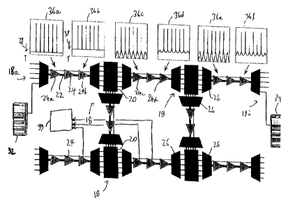
Figure 1 shows a ''~VDM optical cozxununicatioas network comprising a
plurality of
intereotunecLed nodCS 18, cash nods comprising arc optical svvttching
artarigerttent 20 Fur
CA 02375706 2002-03-11
7
per!'uru~iug routing of signals across the network. The nodes are. conne~,rted
together by optical
fibers 22 along which optical amplifiers 24 are placPri. The fibers 22 carry
W'blYl optical
signals, and each node comprises multirlexingldemultiplexing units 26 wLic~lt
provide the
chancels of tJ~.e WDNI system nn individual flbez5 to tLa switching
arrangcmcr~t 20. The
switching arrangement may switch individual cluurxtels or else bands of
channels.
The network enables equipment 32 at a source node 18a (not shown in Wll) to
communicate with cuuipment 34 at a dcsdxiation node 18b (not shown in full).
'.t'hP eduipment
32, 34 is a~.~y device r~rhich provides optical signals for txansmissinn over
the netwozlC or which
is Nrovidcd for receiving signals from the network.
to Each node 18 may be able to pPrfnrm a regenezation function Iuz~ some of
the signals
passing through the code:. This involves conversion of the signal from the
optical domain to
the electzieal domain, with subsequcnl coizversion back into the optical
domain. The
regez~Prarion function is typically carried out by transponders, which
perforzxt not only receiving
and transmitting Iuncl,ions, but also cr~able wavelen~ translations to bP
carried out. This
!5 e:uahles different sections of the selected path between t.hP source and
destination nodes lu use
different carrier freduencies, which may bP re,~uired by the netwozk
mauaxCment system,
which allocates bandwidth. rn the communication paths.
Although Fiyre: 'I only shawS the source aua Jcstinadon nodes os providing
signals to,
or taking signals from the nelwurk, each ztode of the netwrork may also have
add/drnp
capability.
Figure 1 also shows the optical specavm o~ the W.1~I1A Signal carded by the
fiber 22, at
various locations through the network. Hint 36a shows the laz'ge Spr~:4al
components at the
channel frequencies, supezimpose~l on a smooth noise floor 38. The plot 36a is
the spectrum at
the output of a first amplifier 24a., and lice nuisa r(7.uor 38 represents
noise introduced by the
~.5 amplifier 7.4a, resulting from ampliCmcl spoutancous emission (h,SE). As
the signal passAc
through amplifiers 24, lhC LIUiSC floor 3$ z-isca, and the plot 36b represents
the spectrum at the
output of amplifier 24b. Although the noise floor is shown as flat, it may be
'heavily slaapcd.
:Fur simplicity, the term "floor" is used in this text to describe any noise
pzoi-ile.
When the signals pass thrny~gh a node 1$, they untlrxko dcmultiplc~ing an,d
3o puultiplexix~.g operations at the unirs zti_ These operations resole in
shaping of the noise floor
38, cad in particular tilhering at the inter-charuml frequencies. This 15
Shown m plot 36c, whicbi
shows the output of amplifier 2~4c. ,~ tliv signal propagates through further
ampliiierc, the
noise level tends lir increase as further ASE is added, as shown in plot 3tid.
For simplicity, a
CA 02375706 2002-03-11
s
uniform increase in the noise floor is shown between plots 36c arid 36d,
although in practice
the added noise will mot gcocrally be constant with respect to wavelength.
The noise undergoes ~ur<her shaping as the signals pass thrnugh additional
nodes 18, as
shown in plot 36e, and the propagation through actctition.al amplifiers 24
again ,iu~wases the
noise level as showzc in plot 3(.,h.
As desnnhed ahwe, a known method of rrlGa,sucicrg tlic signal to noise zyatio
is to derive
the channel noise level by analysing the infer-c;luuanel noise level. rn the
case of plots 36a and
3fib, a simple interpulaliuca lretwccn the inter-chfmnel noise levels on
either side of a eha~nnPl
will give au ac;cuc.ate estimation of the ehann~1 noise level. However, whran
there: hoc heen
o,oisc shaping, ns in plots 36c to 36f, the noise no longer hay a constant
slope, so that linear
interpolation between the inter-channel noise levels C.1APS not give an
aCCw~'ate W diualxuu of the
channel noise level. Thus, the (.).S I N t( is not an accuzate estimate of
tliC OSNR. Tt is, however,
desirable to obtain signal tn noise ratio measurciuacrt usip analysis of the
spectral content at
ivter-channel frequencies, because: umasur4ment of the spectral content caxc
be carried out
relatively easily.
Fixure 2 shoves is more detail plots 36b to 36d of Figure: :l, tn Pxniain the
Calculation
process for cvaluuting the true optical signal to noise ratio. In order to
determine Ilic uUlical
signal to noise ratio (OSNR) at a desirPrl Ineat~on within the netwoa'k, fur
cx~uiylo at the output
crf amplifier 2.4~i represented by plot 3bd, the uplic:al signal to inter-
channel noise ratio
(c_WTNR) upstream of the Firsmuclc 18, for example at the output of annplifier
2db (represe.nte~d
by plot 36b), is first (~GLG11111t1Bd. This is derived from xneasurezzient of
the c.hannPi signal level
r~ aucl llrG channel noise level B, the latter bei~ag determined by
iz~tPrrofating the inter-channel
noise levels I31 and ~~, from each side of the channel. This is still an
accurate deternulnatiun dl
the amplifier 24b as no noise shaping ha.s yet affected the optical si~ial, so
that D-(B~ + Bz)/2.
'.Che OSINR is representP.ct ac ~ in plot 3a'b. Then, the uplic;al signal to
inter-chaancl noise ratio
(051N1t) is determined at Lhe downstream output of the first node 18, ix~ this
example at the
otrrpnt of amplifier 24c. This is roprracuted as y in plot 36c and is derived
from the channel
signal level C and llc i~itolpolatcd noise level D. The OSIIVR is also
detcrmi..nP.o at the desired
location, which in this example is the output of amplifier '7.4ct. 'this is
represented as x in plus
3o :D6d and is derived froxu the channel signal level H. and the interpolated
noi~5e 1CVC1 P. Finally,
the OSNR at floe desired lacatiozc., represented as w in plot 36c1, is
estimated from the channel
signal level E and an estim~atP~i channel noise level F° which tdkGS
into account noise shaping_
'fhe use of OSINR values Cccaulcs the calculation of noise level to take into
account the
general attenuation (or gain) within the systc~on. rn other words, the noise
shaping can not be
~.. ,....,.w. ~..e~........,.,.-.~".,W-~".~.. .m.~.w.........~. .....M...
....._.........__........
CA 02375706 2002-03-11
9
aclrr~uinod only ~t-om mcasurcznents of inter channel noise levels, but must
also take i.z~tn
account attenuation across the frequency spectrum. The US11VH valnrs rake into
account the
signal levels at the channel frequ~extcies, and thereby take account of this
anet~uauon.
For the simplified case where tb.P siEnal level at tile ehanx~el frrducuc_y is
the SamC at
locations 24b, .7.4e and h4d, as shown schematically in Figure 2, the
estimated channel noise
le~rel F' is obtained as:
F' = B +(F-D), auJ. the OSNI; is obtained from E and F'. Zn practice, the
OSINR values
x, y, z enable the OSNR value w to be obtained e~ren when tlae general signal
levels are
~Yifferent at dif~fercnt locations. 4f course, OSrNR values do trot need to he
calculated, as the
C3SNR calculation can be derived from the signal measurements I;A, to F)
witJaout actually
zxeeding to calculate the US1NK valnPC x, y, ~.
.F,ach ortical ampliflez in the network is ,prvvi~tc~3 with t7hc apparatus for
measuring
inter-channel noise level and fut. jmeasuring the chatmcl signal lev~1. 8y
measuring the OSNR
before any noise slrapiaig occurs (at the upstrcaxn input of the first node),
then axaeasuring the
i5 OSINR at each subsequent amplifier, the amount of noise added to the Signal
by each
s.ubsequcnt amplifier can be deter~nnined, and the OSNR at P,aah amplifier
calculated.
Although not shown ix~. riPra.il m t;'igure 1, the upstream and dvwmUCam
asnplificzs (for
example 24b and 7.4e) may comprise part of the node ilselx, fur cxaz~nple
compzising a pre
amrlifier and a pose-amplifier.
Figure 3 slruws schematically one possible apparatus enabling the signal level
to he
z~netusura~l Gitl~r at the channel frequencies or at the inter-channel
frequenci.Ps. At the output of
the amplifier 24, a eplitter 40 is provided, which wares a propo~ion of the
signal to a lunralrlc
filter X1.2, the output of which is sr~hj@.cted to signal measurement, fUl'
Gxauzple using a
photodiode. arrangement 44. C~tical signal measureuiaut may <also be carried
out using a"
25 l~abry-Pesat interferometer sensor. Ocher upticaa spectmm analysis
techniques will be well
known to those skilled in tlic ~c, and the izwcntion can be irnpl~mented by
any such apparah~a
providing it erm ba tuned to zncasurE signal levels at channel and inter-
channel frP,rloPncies.
As discussed above, a parameter which is increasingly heing used for
wepre5enting the
performance of optical networks is the (1 valve:. This can be measured aClcr
co~t'version froze
3o the optical domain to the electrical dam.ain, and is therefore easily
c:arriCr~ nut at rcgczrerator
sites, within the nodpc 1 X.
Fiyre 4 shows a possible O measureiuct~t ~u'cuit which can bo used at the
regenerator
rite. The receivCr GO of a rcgcneratar supplies th~ signal to a clock
extraction cineuit 62, which
~;lock5 LhC ~cision circuits of the Q measurement circuitry. "fhe clock
extrdelion CiTCUitt 62 t;au
CA 02375706 2002-03-11
pruvidc aTlaNtive clock recovery, so that the error measurement is bit rate
independent. '.I'hP
Gr.~ror ratio is obtained by comparing the measured signal from one dericinn
circuit D1
(essentially a comparator) which uses a fixed derision rhrechold ~''~ (the
z~ornlal operating
point for the decision threshold of the rha.nnel j with the measured signal
fium another decision
5 circuit f~2 whych uses a variable decision threshold Vv,~~~.
The variable decision thrcsliula sca.iis various values, in known manner. The
further the
decision threshold is from ttic ca~ulxo of the cyc, the higher the error
:ratio that is measured.
The lwu measured signals r~rc supplied to an Oft element ei6 which providp:~
an output
Irulse when the inputs arc different. Each output pulse represents an ezrnr,
which assumes the
1o normal operating point Vprovides an PT-r~r tree signal, so that all
differences lu lLis nm
errors. The pulse rate is measured r~ nhrain the BEIZ fbit Crrur .raliu) for
different decision
threshold voltages. 'These BER values can be used to dGLCi'~~ritlc tlZC Q
value, csscz~tit~lly by a
process of extrapolation, and this pru~css will be well known to tho3e skilled
in the art. High
error ratio counts are of cuurse less accurate thazi Iow error ratio eouxats
if the errors cxoss the
ikurulal decision threshold. However, in this case, there are still ~an.any
more errors frorrx the
comparator with the offset threshold these the compar.~tnr with the norrllal
tht~eshold allowing
the eutimation of Q to remain reasvza.ahly accurate.
The output of the fixed threshold deClslon circuit pruvidcs the normal
receiver output
C8, which m then used to drive the transualler of chc converter, either at the
game or a different
optical frequency (~lC~oudin~ oz~ vvhcthcr frequency translation is
r~eduired)_
This Q mcasuremcnt circuitry can be provided at each node. However. the
amplifiers
2~ do not require opto electric cvz~x~ersion, acrd theretnrr do not have the
required rec:eivcr 60.
IIowcvcr, the accurate knowledge of the optx~al signal to noise ratio at each
amNlirer sift
enables the Q value at that rote also to be determined. Thi' i~uvolves
comparing the optical
~s signal to noise ratio at the amplifier site with lhc OSNR at flat
preccdiaag node, at which the Q
value is lcntown. The de~rtalatiuu of the 05NIt can then be used to modify the
Q valTaP, to
provide a reasonably ac:ow:ate cstin xation of the Q value at the atr~plifier
site_
Il sllould be apprcciatcd by those skilled zn the art that the dPrPrmination
of the Q value
ehroughout the network is e>ztirely optional, and in many cases fault
detection and luc;ation can
3o be brased solely an the optical signal to noise ratio calculations at eat:h
silo willuu the nctvvork.
As will 1~ aPrarent from the above descriptiuu, the calculation of the OSNR at
any
lOCatlon ~~'-fllaTTeS data to be provided to that luualiuu relating to signal
mcasurexnents upstream
and downstream of the nudes in the path of the signal to that location. This
may hp c:oordinated
by a network luauagcmcnt systcrr<> shown schematically as 35~ is .~iglarP y .
The system receives
... . . ...m ... . T .. .~. ....... .. .... , .. ....r.~ e. ... ~..... .. .
...._... . ._...
CA 02375706 2002-03-11
m
iliputs frou~ all of the locations at which OSNR is zequ3red, and from all of
the loeatinnc
upstream and downstream of each made. Only three inputs to tk~P r~e~ruvnrk
management system
39 same shown in Figure 1 for clarity. The network nlanagemant system includes
suflw~u~ fvr.
performing the analysis ox the, in,put.S in order to catculale the OSN~', at
each locatioa.
s AItPrnatively, a distributed system may be implCUiGutzcl, by which Gash node
passes an
the measurements upstzieaur. autl duwust~~caxn of the node to the aext nude in
the signal path.
7.'his lnforma,liun uu~y, for exaa~aple, be ctu~ried by the Optical Service
Channel. Zn, the:
distributed systcna, ouch amplifier site at which OSNR is to 'hP ralanlatpc!
will include a
proccssox apparatus havinS an input for rece.~iv;.~ng signal ).P'VPi rtat» at
frequencies bout at and
in-l~tween the channel frequencies far Ic~cati~ns immediately upstream and
downsLrCraui of
each node in the path of the nrtical signal and at the lvcraliucz at wliich
the optical signal to
nnlCP fatto 1C to be measured. The IJ~t7CCSbUI WJ,11 /~l'OCCSS the inputs to
determine the OS~1R at
the loCatioz~, taking ilrlu account the noise shaping of the multiplexing
~dlor demultxple~cing
Li<t;Yli:G uT 111G 110C1G5 In thG pElth of the optical Signal.
1~ Various modifications will be apparent to those skilled an thr. art.
_..a _.... .... .~...~...:......,~...~..., .~...w..__.. ._
....~..,.~......",..~..:.".:.,.n
......~,..~.~._~....~.._.._.......~.~.._...._....... .