Note: Descriptions are shown in the official language in which they were submitted.
CA 02375730 2001-11-29
WO 00/76156 PCT/US00/15266
-1-
TITLE OF THE INVENTION
ARCHITECTURE FOR A HYBRID STM/ATM ADD-DROP MULTIPLEXER
CROSS REFERENCE TO RELATED APPLICATIONS
NOT APPLICABLE
STATEMENT REGARDING FEDERALLY SPONSORED RESEARCH OR
DEVELOPMENT
NOT APPLICABLE
BACKGROUND OF THE INVENTION
The invention relates generally to communication
systems, and more specifically to an architecture for a
hybrid STM/ATM add-drop multiplexes.
As it is generally known, SONET (Synchronous
Optical Network) defines a set of standards for a
synchronous optical hierarchy that has the flexibility
to transport many digital signals having different
capacities. A corresponding international synchronous
digital hierarchy (SDH) standard provides a set of
definitions analogous to those of SONET. The synchronous
nature of SONET is provided by a receive side and a
transmit side clock in each network element (NE). In
order to synchronize the receive and transmit clocks, a
SONET network element, such as an add-drop multiplexes,
includes circuitry to recover clock signals from various
sources that may be available, and to distribute highly
accurate clocks internally based on such recovery.
A central timing source provides a Building
Integrated Time Source, also referred to as a "BITS"
clock, that may be provided out-of-band to each network
element in a SONET ring. If a network element is for
some reason not able to receive the BITS clock directly,
an embedded clock may be recovered by that device from
an incoming line that should reflect the centrally
provided BITS clock.
CA 02375730 2001-11-29
WO 00/76156 PCT/US00/15266
-2-
The basic building block in SONET is a synchronous
transport signal level-1 (STS-1), which is transported
as a 51.840-Mb/s serial transmission using an optical
carrier level-1 (0C-1) optical signal. Higher data rates
are transported using SONET by multiplexing N lower
level signals together. To this end, SONET defines
optical and electrical signals designated as OC-N
(Optical Carrier level-N) and STS-N (Synchronous
transport signal level-N), where OC-N and STS-N have the
same data rate for a given value of N. Accordingly,
just as STS-1 and OC-1 share a common data rate of 51.84
Mb/s, OC-3/STS-3 both have a data rate of 155.52 Mb/s.
Information transported via an STS-1 signal is
organized as frames, each having 6480 bits (810 bytes).
An STS-1 frame includes transport overhead and a
Synchronous Payload Envelope (SPE). The SPE includes a
payload, which is typically mapped into the SPE by what
is referred to as path terminating equipment at what is
known as the path layer of the SONET architecture . Line
terminating equipment, such as an OC-N to OC-M
multiplexer, is used to place an SPE into a frame, along
with certain line overhead (LOH) bytes. The LOH bytes
provide information for line protection and maintenance
purposes. The section layer in SONET transports the STS-
N frame over a physical medium, such as optical fiber,
and is associated with a number of section overhead
(50H) bytes. The SOH bytes are used for framing,
section monitoring, and section level equipment
communication. Finally, a physical layer in SONET
transports the bits serially as either electrical or
optical entities.
The SPE portion of an STS-1 frame is contained
within an area of an STS-1 frame that is typically
viewed as a matrix of bytes having 87 columns and 9
rows. Two columns of the matrix (30 and 59) contain
fixed stuff bytes. Another column contains STS-1 POH.
The payload of an SPE may have its first byte anywhere
CA 02375730 2001-11-29
WO 00/76156 PCT/US00/15266
-3-
inside the SPE matrix, and, in fact may move around in
this area between frames. The method by which the
starting payload location is determined is responsive to
the contents of transport overhead bytes in the frame
referred to as H1 and H2. H1 and H2 store an offset
value referred to as a "pointer", indicating a location
in the STS-1 frame in which the first payload byte is
located.
The pointer value enables a SONET network element
to operate in the face of certain conditions which may,
for example, cause the STS-1 frame rate to become faster
or slower than the SPE insertion rate. This situation
may arise when the clock of the NE must be derived from
a relatively less accurate clock source, in order to
continue operation, when a more accurate source, such as
the BITS clock itself, has been lost. In such a case,
an extra byte may need to be transmitted in what is
known as a negative justification opportunity byte, or,
one less byte may be transmitted in a given STS-1 frame
so as to accommodate the SPE, thus causing the location
of the beginning of the payload to vary.
Various digital signals, such as those defined in
the well-known Digital Multiplex Hierarchy (DMH), may be
included in the SPE payload. The DMH defines signals
including DS-0 (referred to as a 64-kb/s time slot), DS-
1 (1.544 Mb/s), and DS-3 (44.736 Mb/s). The SONET
standard is sufficiently flexible to allow new data
rates to be supported, as services require them. In a
common implementation, DS-is are mapped into virtual
tributaries (VTs), which are in turn multiplexed into an
STS-1 SPE, and are then multiplexed into an optical
carrier-N (OC-N) optical line rate.
The payload of a particular SPE may be associated
with one of four different sizes of virtual tributaries
(VTs). The VTs are VT1.5 having a data rate of 1.728
Mb/s, VT2 at 2.304 Mb/s, VT3 at 3.456 Mb/s, and VT6 at
6.912 Mb/s. A superframe consists of four STS-1 frames,
CA 02375730 2001-11-29
WO 00/76156 PCT/US00/15266
-4-
and is used to transmit a VT. The alignment of a VT
within the bytes of the payload allocated for that VT is
indicated by a pointer contained within two VT pointer
bytes, which contain a pointer offset similar to the
STS-1 pointer described above.
Existing add-drop multiplexers (ADMs) are SONET
multiplexers that allow DS-1 and other DMH signals to be
added into or dropped from an STS-1 signal. Traditional
ADMs have two bi-directional ports, and may be used in
self-healing ring (SHR) network architectures. An SHR
uses a collection of network elements including ADMs in
a physical closed loop so that each network element is
connected with a duplex connection through its ports to
two adjacent nodes. Any loss of connection due to a
single failure of a network element or a connection
between network elements may be automatically restored
in this topology. Existing ADMs have additionally
included a cross-connect matrix for directing STM
signals from one interface to another. Such a cross-
connect matrix is referred to as an STM switch fabric.
The manner in which specific STM signals are directed
between interfaces of the STM switch fabric depends on
how the network bandwidth has been "provisioned" to the
various customers using the network. The path of a
signal through a given cross-connect matrix is
statically defined based on provisioning information
provided from a central office or "craft" technician.
As mentioned above, SONET provides substantial
overhead information. SONET overhead information is
accessed, generated, and processed by the equipment
which terminates the particular overhead layer. More
specifically, section terminating equipment operates on
nine bytes of section overhead, which are used for
communications between adjacent network elements.
Section overhead supports functions such as: performance
monitoring (STS-N signal), local orderwire, data
communication channels (DCC) to carry information for
CA 02375730 2001-11-29
WO 00/76156 PCT/US00/15266
-5-
OAM&P, and framing. The section overhead is found in
the first three rows of columns 1 through 9 of the SPE.
Line terminating equipment operates on line
overhead, which is used for the STS-N signal between
STS-N multiplexers. Line overhead consists of 18
overhead bytes, and supports functions such as: locating
the SPE in the frame, multiplexing or concatenating
signals, performance monitoring, automatic protection
switching, and line maintenance. The line overhead is
found in rows 4 to 9 of columns 1 through 9 of the SPE.
Path overhead bytes (POH) are associated with the
path layer, and are included in the SPE. Path-level
overhead, in the form of either VT path overhead or STS
path overhead, is carried from end-to-end; it is added
to DS1 signals when they are mapped into virtual
tributaries and for STS-1 payloads that travel end-to-
end. VT path overhead (VT POH) terminating equipment
operates on four evenly distributed VT path overhead
bytes starting at the first byte of the VT payload, as
indicated by the VT payload pointer. VT POH provides
communication between the point of creation of an VT SPE
and its point of disassembly.
STS path terminating equipment terminates STS path
overhead (STS POH) consisting of nine evenly distributed
bytes starting at the first byte of the STS SPE. STS POH
provides for communication between the point of creation
of an STS SPE and its point of disassembly. STS path
overhead supports functions such as: performance
monitoring of the STS SPE, signal labels (the content of
the STS SPE, including status of mapped payloads), path
status, and path trace. The path overhead is found in
rows 1 to 9 of the first column of the SPE.
Asynchronous Transfer Mode (ATM) is a cell-based
transport and switching technology. ATM provides high
capacity transmission of voice, data, and video within
telecommunications and computing environments. ATM
supports a variety of traffic types, including constant
CA 02375730 2001-11-29
WO 00/76156 PCT/US00/15266
-6-
bit-rate (CBR) traffic - like full-motion video and
voice - where delays and cell loss cannot be tolerated.
ATM also supports variable bit-rate (VBR) applications
- like LAN traffic and large file transfers - where
delay can be tolerated.
ATM establishes virtual connections which may be
shared by multiple users. Each ATM virtual connection
is identified by a combination of a Virtual Channel
Identifier and a Virtual Path Identifier, referred to as
a VCI/VPI value. ATM is a transport technology that
formats all information content carried by the network
into 53-byte cells. Since these cells are short in
length and standard in size, they can be switched
through network elements known as ATM switches with
little delay, using what is referred to as an ATM switch
fabric. Since various types of traffic can be carried
on the same network, bandwidth utilization can be very
high. These characteristics make the network very
flexible and cost effective.
An ATM switch fabric operates to direct ATM cells
from one interface to another. For a given received
cell, the specific output interface of the ATM switch
fabric is determined in response to a VCI/VPI value
contained within the cell. Virtual channel and virtual
path routing information is dynamically modified in the
switch fabric as connections are established and torn
down in the network. In this way the ATM switch fabric
operates in response to dynamically changeable virtual
connection information.
ATM cells may be encapsulated and transmitted over
SONET for example using STS-1 or STS-3c, which is a
concatenation of three STS-1 signals. STS-1 transports
may generally be concatenated, and the combination then
referred to as STS-Nc, where N is the number of STS-1
signals that are combined. In the case of STS-3c, the
SPE of the resultant STS-3c frame consists of 3 x 783
bytes, together with POH. The concatenated STS-is are
CA 02375730 2001-11-29
WO 00/76156 PCT/US00/15266
multiplexed, switched, and transported as a single unit.
An overhead byte of the STS-3c frame transport
overhead, referred to as the H4 byte, contains an offset
indicating the number of bytes between the H4 byte and
the first ATM cell that is contained in the SPE.
In many cases customers require support for both
ATM switching and STM switching in their communications
systems. However, devices provided by vendors to
support SONET have typically lacked the capability to
also support ATM. In particular, typical existing ADMs
have supported only SONET rings, while existing ATM
switches have generally supported only ATM.
Accordingly, if a customer has needed both SONET and ATM
networks, they have necessarily had to purchase
dedicated SONET equipment (ADMs), in addition to ATM
switches. This is costly in terms of necessitating
multiple devices. In addition, most customers cannot
predict what their future communications requirements
will be when they buy one piece of equipment. Because
existing systems have been restricted to supporting only
one of either SONET or ATM switching, they have not been
flexible or scalable with regard to adding support for
the other protocol. As a result of such inflexibility,
changes in customer requirements may require the
purchase of completely new devices to support a
previously unsupported protocol.
Accordingly, there is a need for a communication
device which combines the functions of a SONET add-drop
multiplexer with the functions of an ATM switch. The
device should be capable of multiple configurations to
support STM only, ATM only, or hybrid STM/ATM operation.
Moreover, the device should be scalable such that
additional functionality may be conveniently added as
the needs of the customer change over time.
CA 02375730 2001-11-29
WO 00/76156 PCT/US00/15266
_g_
BRIEF SUMMARY OF THE INVENTION
An architecture for a hybrid STM/ATM add-drop
multiplexer is disclosed. The disclosed architecture
includes an interconnection system for a network
element, having at least one line unit slot, a switch
fabric slot, and two or more service unit slots. The
line unit slot is connected as a hub to the switch
fabric slot and the service unit slots in a first star
interconnection configuration. The switch fabric slot
is connected as a hub to the line unit slot and the
service unit slots in a second star interconnection
configuration. In a preferred embodiment, the switch
fabric slot and one of the service unit slots comprise
the same slot, thus permitting flexible configuration of
the device. To support a configuration providing non-
STM switching, the switch fabric slot is operable to
receive a switch fabric unit that includes a non-STM
switch fabric.
In an illustrative embodiment, a control unit slot
is provided in the interconnection system, and connected
as a hub to the line unit slot, the switch fabric slot,
and the service unit slots to form a third star
interconnection configuration. Each star
interconnection configuration for example consists of
dedicated point to point connections between the hub and
each other slot in the configuration. The point to
point connections employ a low voltage, complementary
signaling mechanism, such as Low Voltage Differential
Signaling (LVDS), in order to achieve high speeds, while
controlling electromagnetic interference (EMI).
Redundant line unit and switch fabric slots are
provided, as well as respective redundant star
configurations, to permit line units and switch fabric
units to be configured in "active/standby" pairs, thus
supporting greater system availability and robustness.
A line unit is also disclosed which may be disposed
within the line unit slot. The disclosed line unit
CA 02375730 2001-11-29
WO 00/76156 PCT/US00/15266
-9-
includes an STM switch fabric, as well as an optical
interface to a SONET ring. The line unit module further
includes two or more service unit interfaces for
coupling the STM switch fabric to point to point
interfaces within the first star interconnection
configuration, so as to permit communication of
information contained within the SONET frames between
the line unit and service units disposed in the service
unit slots. The disclosed line unit further includes at
least one ATM interface, for communicating ATM cells
between the line unit and an ATM switch fabric unit
disposed in the switch fabric slot. The disclosed line
unit provides what are referred to herein as the
"service affecting" functions of the device with regard
to STM. STM service affecting functions are those
functions necessary to maintain continued operation of
STM communication through the device. Accordingly, to
provide fault recovery and avoid STM service
interruptions, the device may be advantageously
configured with an active/standby pair of line units.
An ATM switch fabric unit is disclosed which may be
installed within the switch fabric slot. The disclosed
ATM switch fabric unit includes two or more service unit
interfaces which are coupled to point to point
connections within the second star interconnection
configuration. During operation of the device, ATM
cells are communicated in ATM cell stream format between
service units in the service unit slots and the switch
fabric unit over the second star interconnection
configuration. The disclosed ATM switch fabric unit
provides what are referred to herein as the "service
affecting" functions of the device with regard to ATM.
ATM service affecting functions are those functions
necessary to maintain continued operation of ATM
communication through the device. Accordingly, to
provide fault recovery and avoid ATM service
interruptions, the device may be advantageously
CA 02375730 2001-11-29
WO 00/76156 PCT/iJS00/15266
-10-
configured with an active/standby pair of ATM switch
fabric units.
A management and control unit (MCU) is disclosed
which may be installed in the control unit slot. The
disclosed MCU communicates SONET overhead information
over the third star interconnection configuration. The
MCU further operates to download executable software
images to service units installed in the network element
over the third star interconnection configuration. The
MCU provides what are referred to herein as the "non-
service affecting" functions of the device.
A service unit for a network element is also
disclosed, which includes a first backplane interface
for connecting with the first star interconnection
configuration within the network element. The first
backplane interface to the first star interconnection
configuration permits transport of STM frames to an STM
switch fabric. The service units include a second
backplane interface for connecting to the second star
interconnection configuration. The second backplane
interface to the second star interconnection
configuration permits transport of ATM cells to the ATM
switch fabric. In a preferred embodiment, the service
unit further includes a third backplane interface to
connect with the third star interconnect configuration
for communication with the MCU within the network
element.
Thus there is provided a communication device which
combines the functions of a SONET add-drop multiplexer
with the functions of an ATM switch. The disclosed
device supports multiple configurations, including STM
only, ATM only, or hybrid STM/ATM operation. Moreover,
the disclosed device is flexible and scalable such that
functionality may be added or modified as the needs of
the customer change over time. The disclosed system
advantageously applies low voltage, complementary
signaling techniques such as Low Voltage Differential
CA 02375730 2001-11-29
WO 00/76156 PCT/US00/15266
-11-
Signaling (LVDS) to provide high speed, serial point to
point links in star configurations. The use of serial
point to point links supports failure isolation, since
failure of a single non-hub unit will not affect the
connections of other units to the hub of the star.
Accordingly, replacement of a non-hub unit is possible
without disturbing the operation of the other units in
the star. The disclosed system supports failure
protection in hub units, such as the line units and ATM
switch fabric units, by providing connectivity for
active/standby unit pairs of the line unit and ATM
switch fabric unit. In addition, by use of multi-
function service unit slots, which can also serve as ATM
switch fabric unit slots, the disclosed system supports
a wide variety of configurations in a minimum amount of
space.
BRIEF DESCRIPTION OF THE SEVERAL VIEWS OF THE DRAWING
The invention will be more fully understood by
reference to the following detailed description of the
invention in conjunction with the drawings, of which:
Fig.l shows module partitioning in an illustrative
embodiment of the disclosed network element;
Fig. 2 shows the layout of slots in an illustrative
embodiment of the disclosed network element
interconnection system;
Fig. 3 illustrates multiple star interconnection
configurations employed in the disclosed network
element;
Fig. 4 shows an illustrative configuration of the
disclosed network element providing synchronous transfer
mode (STM) support;
Fig. 5 shows an illustrative configuration of the
disclosed network element providing asynchronous
transfer mode (ATM) support;
Fig. 6 shows an illustrative configuration of the
disclosed network element providing asynchronous
CA 02375730 2001-11-29
WO 00/76156 PCT/US00/15266
-12-
transfer mode (ATM) support and synchronous transfer
mode (STM) support;
Fig. 7 is a functional block diagram of an illustrative
line unit employed in the presently disclosed network
element;
Fig. 8 is a block diagram illustrating the STM and ATM
inbound datapath within the line unit;
Fig. 9 is a block diagram illustrating the STM and ATM
outbound datapath within the line unit;
Fig. 10 is a block diagram of a control architecture for
the line unit;
Fig. 11 is a block diagram of a signal routing ASIC;
Fig. 12 is a block diagram of an extended
synchronization module;
Fig. 13 is a block diagram of software and hardware used
to download a software image into a management and
control unit;
Fig. 14 is a block diagram showing hardware components
within a management and control unit and an intelligent
service unit;
Fig. 15 is a block diagram showing interfaces of a
management and control unit;
Fig. 16 is a block diagram showing a gateway network
element and a remote network element; and
Fig. 17 is a flow chart showing steps performed to
download a software image to a network element.
DETAILED DESCRIPTION OF THE INVENTION
A network element (NE) architecture is disclosed
which conveniently and efficiently combines the
functions of a SONET add-drop multiplexer (ADM) with the
functions of an ATM switch. As shown in Fig. 1, the
disclosed network element 10 may be physically embodied
as a set of hardware ~~units" interconnected across an
interconnection system, also referred to as a backplane.
The units, for example, include line units (LU) 30, a
management and control unit (MCU) 32, ATM switch fabric
CA 02375730 2001-11-29
WO 00/76156 PCT/US00/15266
-13-
units (ATMU) 34, and service units (SU) 36. The ATMU 34
provides ATM cell-relay related functionality, such as:
VP and VC switching, segmentation and reassembly,
signaling, routing, call control, traffic management,
and Operations Administration, Management, and
Provisioning (OAMP). In this regard, the ATMU may
specifically provide address translation, an application
programming interface (API) for user to network
interface (UNI) signaling, an interim local management
interface (ILMI) server, full ILMI and user network
interface/network to network interface (UNI/NNI)
signaling stacks, a private node-to-node interface
(PNNI) server for routing, and connection admission. In
an alternative embodiment, such ATM functionality may be
split across two separate unit types: ATM Switch units
(ATMSU) containing primarily the ATM switch fabric, and
ATM Processing units (ATMPRU) providing other ATM
functions.
In another alternative embodiment, an Internet
protocol (IP) switch fabric unit may be substituted for
one of the ATM switch fabric units. The IP switch
fabric unit performs switching (also known as rerouting")
at the IP layer of the TCP/IP protocol stack, using what
is referred to herein as an IP switch fabric. The IP
switch fabric unit may also provide an ATM switch
fabric, together with such ATM functionality as
described above.
The network element 10 provides (1) a SONET line
interface on a line side 15, (2) connection of ATM
traffic from either the line side 15 or a service side
20 to an ATM switch fabric unit 34, (3) connection of
STM traffic from either the line side 15 or the service
side 20 to STS/VT switch fabrics within the line units
30, (4) various service interfaces on the service side
30 through the specific service units 36. The ATM
switch fabric unit 34 performs activities associated
with ATM cell-relay. These for example include VP and
CA 02375730 2001-11-29
WO 00/76156 PCT/US00/15266
-14-
VC switching, signaling, routing, call control, and
traffic management.
The line units 30 may support various SONET optical
media line interfaces, such as OC-3, OC-12, or any other
suitable optical interface. The line unit provides
interfaces to the ATM switch fabric unit 34 from a SONET
ring on the line side 15, as well as to the various
service units 36. The line unit also includes an STM
switch fabric 39 capable of performing STM switching at
both the STS and VT levels. Examples of ATM switch
fabric unit 34 include modules providing connectivity to
the line units 30, as well as to the service units 36,
and which also include an ATM switch fabric 41.
Service units 36 include modules supporting various
telecommunication or data communication interfaces to
the service side 20, including for example DS-1, DS-3,
Token Ring, FDDI (fiber distributed data interface),
lOBaseT, 100BaseT, lOBaseF, or 100BaseF Ethernet, EC-1
(electrical carrier 1, also referred to as STS-1
electrical, or STS-1/EC-1), OC-3, OC-12 or any other
suitable service. The service units 36 may communicate
with the ATM switch fabric 41 installed in the ATM
switch fabric unit 34 of the network element, as well as
with the STM switch fabrics 39 contained within the line
units 30. Accordingly, service units 36 for the network
element 10 contain interfaces within the network element
which may be considered to fall within three categories:
STM, ATM, and STM/ATM. For example, STM service unit
36a formats data received from the service side 20 into
STS frames to be forwarded to the line units 30, while
ATM service unit 36c formats data received from the
service side 20 into ATM cell streams to be forwarded to
the ATM switch fabric unit 34. Since each service unit
36 is connected to both ATM and STM services, a single
STM/ATM service unit 36b may simultaneously use ATM and
STM switching services by selectively communicating the
CA 02375730 2001-11-29
WO 00/76156 PCT/US00/15266
-15-
data it receives to the line units 30 and/or the ATM
switch fabric unit 34.
Management and control unit 32 includes a subsystem
employing a microprocessor 33 coupled to microprocessor
bus 37. The illustrative MCU 32 provides a basic
control infrastructure for the network element 10, using
what is referred to herein as a "serialized hardbus".
During operation of the network element 10, the
components of the serialized hardbus convert a parallel
bus communication protocol into a master/slave,
serialized communication between the MCU 32 and the
other units in the network element 10. A serialized
hardbus master logic unit 35 is coupled to
microprocessor bus 37 of the MCU and maps control and
status registers and/or memory locations of other units
in the network element onto the microprocessor memory
map. Units within the device 10 which are managed by
the MCU 32 include serialized hardbus termination logic.
The serialized hardbus also provides notification of
certain autonomous events and/or alarms, occurring on or
detected by other units, by interrupting the
microprocessor 33.
In addition to the serialized hardbus, the MCU 32
uses a SONET overhead link from each line unit 30 and
service unit 36, to support maintenance communications
such as Data Communications Channel (DCC) and OrderWire
information. The MCU 32 further includes various
management and control capabilities, such as DCC and
Orderwire processing functionality, which may include a
combination of hardware and software, and which are used
to process the received maintenance information.
Fig. 2 shows an illustrative slot layout 40 for the
disclosed interconnection system. The slot layout 40 of
Fig. 2 includes several different types of slots,
specifically line unit slots 42, management and control
unit slot 44, and service unit slots 46. The service
unit slots 46 include two slots 48 which may also be
CA 02375730 2001-11-29
WO 00/76156 PCT/US00/15266
-16-
used as ATM switch fabric slots. The slots 48 are
accordingly also referred to as switch fabric slots, or
ATM switch fabric slots. The slots shown in Fig. 2 are
each operable to receive hardware units as described in
Fig. 1 of the corresponding type. For example, line
unit slots 42 are operable to receive line units 30,
service unit slots 46 are operable to receive service
units 36, ATM switch fabric unit slots 48 are operable
to receive ATM switch fabric units 34 or service units
36, and MCU slot 44 is operable to receive the MCU 32.
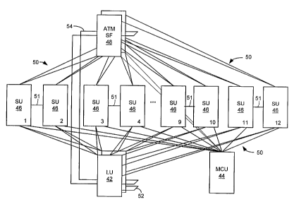
Fig. 3 illustrates the multi-star architecture of
the disclosed interconnection system. As shown in Fig.
3, a number of point-to-point connections 50 form star
configurations having the management & control unit slot
44, line unit slots 42, and ATM switch unit slots 48 as
hubs. In a preferred embodiment, the point-to-point
connections 50 are implemented using a low voltage,
complementary signaling technique to achieve high
speeds, such as Low Voltage Differential Signaling
(LVDS). In addition, the point-to-point connections 50
are terminated in the backplane, without the presence of
a service unit within any of the respective service unit
slots 46. Accordingly, no additional physical
termination is required for empty one of the service
unit slots 46.
In the depiction of Fig. 3, and as shown in Fig. 2,
two of the service unit slots 46 are the same as ATM
switch fabric slots 48. Accordingly, when ATM switch
fabric slots 48 are used to connect ATM switch fabric
units, these same slots may not simultaneously be used
to install service units. However, as shown in Figs. 2
and 3, those two "multifunction" slots may alternatively
be used to connect service units to the device in
configurations where the ATM switch fabric units are not
needed.
More specifically, in a preferred embodiment, each
line unit slot 42 has two star configurations emanating
CA 02375730 2001-11-29
WO 00/76156 PCT/US00/15266
-17-
from it. An STM datapath star communicates STM type
data with each of the service unit slots 46. The second
star emanating from each line unit slot 42 is a
synchronization star for conveying a frequency reference
and a frame alignment pulse (FP) to the service unit
slots 46, in order to synchronize STM communication
between each service unit and the STM switch fabrics
within the line units. An extended synchronization
module (ESM) may be provided to accept and distribute an
extracted clock from the service unit slots 46 or,
alternatively, a BITS clock from further
interconnections within the device. The ESM is for
example implemented on a sub-board module which is
electrically and mechanically coupled to an alternative,
enhanced version of the illustrative line unit.
In addition to the STM datapath and synchronization
interconnection stars, a private datapath 52 is provided
for communicating STM data between active and standby
line units installed in respective ones of the line unit
slots 42. The private datapath 52 facilitates a pass
through path between the line units which may be
required under certain conditions.
Further, in the illustrative embodiment of Fig. 3,
the line unit slots 42 each have a datapath connection
54 to each of the ATM switch fabric slots 48. This
interface supports ATM cell stream traffic between the
ATM switch fabric slots 48 and the line unit slots 42.
During operation of the device, ATM traffic from both
line unit slots 42 (active and standby) is forwarded to
each of the ATM switch fabric slots 48. Accordingly,
per unit fault protection of the units in the line unit
slots 42 and ATM switch fabric slots 48 may be provided
independently, on a unit by unit basis.
Further, in the illustrative embodiment of Fig. 3,
the MCU slot 44 has two star interconnect configurations
emanating from it. First, an MCU control star is
provided to support the serialized hardbus between the
CA 02375730 2001-11-29
WO 00/76156 PCT/US00/15266
-18-
MCU and each other unit in the device. Second, a SONET
overhead star supports communication of SONET overhead
information, such as DCC and Orderwire data, as well as
other information in the section, line, or path overhead
portions of a SONET signal, between the MCU and other
units in the device. The SONET overhead star connects
the MCU slot 44 to each other slot in the device, via
respective ones of the point to point connections 50,
thus enabling communication of SONET overhead between
the MCU and any other unit in the device, including
service units installed in the service unit slots 46.
The MCU slot 44 is further provided with a software
image download interconnection with the ATM switch
fabric slots 48 to facilitate communication of software
executable image data between an ATM switch fabric unit
installed in the ATM switch fabric slots 48 and the MCU,
for example using the High-Level Data Link Control
(HDLC) protocol. Such software executable image data
may further be communicated from the MCU to individual
ones of the services units installed in the service unit
slots, over the serialized hardbus.
The ATM switch fabric slots 48 each have a datapath
star emanating from them to all other service unit slots
46. Because these ATM datapath stars are routed to the
other service unit slots 46 independently from any other
star configuration, the cost of adding ATM features is
independent of the costs associated with other
functionality provided by the device.
The disclosed interconnection system supports ATM
VP Path Switching within an active ATM switch fabric
unit coupled to one of the ATM switch fabric slots 48,
through the datapath connection 54. The datapath
connection 54 between each of the ATM switch fabric
slots 48 and both line unit slots 42 enables maintenance
of a current switch state in both of the ATM switch
fabrics within ATM switch fabric units in the switch
fabric slots 48. Unlike support provided in the device
CA 02375730 2001-11-29
WO 00/76156 PCT/US00/15266
-19-
for the SONET Unidirectional Path Switched Ring (UPSR),
in which the pass through path is independently carried
between the line units over the private datapath 52, the
VP pass through path is internal to an active ATM switch
fabric unit. Accordingly, each ATM switch fabric slot
48 supports full ATM bandwidth to and from each line
unit slot 42 simultaneously.
Additionally, the ATM switch fabric slots 48
connect with an ATM Control Bus which extends to two of
the service unit slots 46 which are adjacent to the ATM
switch fabric slots 48, such as the service unit slots
labeled SU09 and SU010 in Fig. 2. This bus enables
division of the ATM switch fabric unit functionality
into separate ATM Switching Unit and ATM Processing Unit
modules. Such a division permits the number of modules
and power allocation for the ATM function to be doubled
by occupying 4 slots with ATM switch fabric units
instead of 2.
For protected services, service unit slots 46 are
allocated in pairs, to support operation of redundant
service units. However, each one of the service unit
slots 46 has independent connections to both the ATM
switch fabric units (in the ATM switch fabric slots 48),
and to both the STM switch fabrics in the line units (in
the line unit slots 42). This allows for a
configuration of up to 12 different unprotected service
units to be supported simultaneously in an STM
configuration, and 10 different unprotected service
units in an STM/STM configuration. Configurable
backplane private connections 51 between selected pairs
of service unit slots 46 are also provided, to support
active/standby service unit pairs, as well as active
standby pairs of ATM switch fabric units in ATM switch
fabric slots 48.
Figs. 4 through 6 illustrate various system
configurations that may be obtained using the presently
disclosed architecture. The disclosed network element
CA 02375730 2001-11-29
WO 00/76156 PCT/US00/15266
-20-
can be configured as an STM system as shown in Fig. 4,
an ATM system as in Fig. 5, or an STM/ATM hybrid system
as shown in Fig. 6, depending on the complement of units
which are employed.
The exemplary configurations of Figs 4-6 include
the following hardware components:
1) line units (LUs) 60a and 60b, which operate as an
active/standby pair, each of which terminates a SONET
ring, for example through an OC-12 connection.
2) a number of service units (SUs), illustrated by the
following specific examples:
STM Service Units 64, which map STM services
provided by the device to their respective STM
service interfaces. Similarly, ATM subtending
ring service units 80e and 80f provide a service
side interface to a SONET ring carrying ATM cells,
and STM/ATM subtending ring service units 90a and
90b provide a service side interface to a SONET
ring carrying both STM and ATM traffic.
Service units 90a and 90b may also be referred to
as ~~Hybrid Service Units", because they provide
both STM and ATM services to their respective
service interfaces. A hybrid service unit
includes three interfaces: an STM internal
interface (to the STM switch fabric), an ATM
internal interface (to the ATM switch fabric), and
a service interface. During operation of a hybrid
service unit, data units such as packets or cells
are forwarded from the interface at which they are
received to either of the other interfaces. Such
forwarding is performed by one or more application
specific integrated circuits (ASICs) and/or a
microprocessor based subsystem. For example, in
CA 02375730 2001-11-29
WO 00/76156 PCT/US00/15266
-21-
another illustrative embodiment, an Ethernet
hybrid service unit is provided. In the Ethernet
hybrid service unit, data units carried in
Ethernet frames are received at an Ethernet
service interface, and are selectively forwarded
to either the STM or the ATM interfaces, based on
information such as addressing included within the
header of each received Ethernet frame.
Similarly, each data unit received at the ATM or
STM internal interfaces may be forwarded to either
the other internal interface, or to the Ethernet
service interface, responsive to information
contained within each data unit, or to
provisioning of individual signals. Hybrid
service units may include any suitable external
service interfaces to the device, including but
not limited to data communications network, such
as Ethernet or ATM, or any traditional
telecommunications system, such as the digital
multiplex hierarchy (DMH) or SONET.
ATM Interworking Service Units 80a, 80c and 80d,
which adapt traditional datacom (10/100BaseT for
example) or telecom (0C-3 or DS-1 for example)
service interfaces to the ATM protocol.
Native ATM Service Unit 80b, which provides an
interface to the ATM services provided by the
device to an ATM service interface, for example an
OC-3 based cell relay connection.
3) ATM switch fabric units (ATMUs) 70a and 70b, which
form an active/standby pair, and which handle ATM VP/VC
switching and other activities associated with ATM cell
relay, such as signaling, routing, call control, and
traffic management.
CA 02375730 2001-11-29
WO 00/76156 PCT/US00/15266
-22-
4) A Management and Control Unit (MCU) 62, which manages
and controls the units within the network element 10.
This unit provides all the administrative interfaces to
the device and processes all the SONET overhead bytes.
The STM system of Fig. 4 includes the two LUs 60a
and 60b, the MCU 62, and some number of STM service
units 64a-64e. Service units 64a and 64b are an
active/standby pair supporting a SONET DS-1 service
interface, service units 64c and 64d are an
active/standby pair supporting a SONET DS-3 service
interface, and service unit 64e supports a SONET OC-3
service interface. The line units 60a and 60b attach
via OC-12 to a SONET ring 61. During operation of the
embodiment shown in Fig. 4, STM signals are routed by
the STM switch fabric in the active one of the line
units 60, between the ring 61 and active ones of the
service units 64 over individual ones of point to point
STS-3 serial links 66.
Fig. 5 shows an ATM configuration of the disclosed
network element, including the two LUs 60a and 60b, the
ATMUs 70a and 70b, the MCU 62 and ATM service units 80a
through 80f. The ATM Interworking service unit 80a
includes a service interface to a 10/100BaseT LAN, the
native ATM service unit 80b includes a service interface
to an OC-3 based cell relay connection, and a pair of
ATM Interworking Service Units 80c and 80d include
service interfaces to a DS-1 frame relay connection.
The service units in Fig. 5 are connected via an
active/standby pair of ATMUs 70a and 70b to a pair of
OC-12 LUs 60a and 60b. The service units 80c and 80d
are configured as an active/standby pair. The ATM
subtending ring service units 80e and 80f provide a
service side interface to a SONET ring carrying ATM
cells.
During operation of the embodiment shown in Fig. 5,
ATM cells carried over STS signals within the SONET ring
CA 02375730 2001-11-29
WO 00/76156 PCT/US00/15266
-23-
61 are routed by the line units 60a-60b over STS-12
datapath connections 81 to each of the ATM switch
fabrics within the ATM switch fabric units 70a and 70b.
The ATM switch fabric units 70a and 70b in turn direct
the ATM cells, based on VPI/VCI values within the cell
headers, to the appropriate destination service units as
indicated by ATM virtual connections established through
the ATM switch fabric.
A hybrid STM/ATM configuration of the disclosed
network element is shown in Fig. 6. In Fig. 6, the STS
signals from the ring 61 which contain encapsulated ATM
cells are routed by the line units 60a-60b to the ATM
switch fabric units 70a-70b. STS signals from the ring
61 that are provisioned to pass through service
interfaces of the device are routed by the line units
60a-60b to the appropriate service units using the STM
switch fabrics contained within the line units 60a-60b.
The service units 64a-64b communicate STM frames with
the line units 60a-60b, while the service units 80a-80b
communicate ATM cells with the ATM switch fabric units
70a-70b. The service units 90a-90b communicate ATM
cells with the ATM switch fabric units 80a-80b, and also
communicate STM frames with the line units 60a-60b.
Fig. 7 is a functional block diagram of an
illustrative line unit 100. The line unit 100 provides
an optical interface to a SONET ring at the line side of
the disclosed network element. The line unit 100 is
shown including a signal routing ASIC 102, which is
coupled to an optical receiver 104, an optical
transmitter 106, ATMU Low Voltage Differential Signaling
(LVDS) receivers 108, ATMU transmitters 110, and an STM
switch fabric ASIC 114. ATMU transmitters 110 and ATMU
receivers 108 are, for example, shown using LVDS
devices. The STM switch fabric ASIC 114 is shown
including service unit transmit interfaces 116 and
service unit receive interfaces 118.
CA 02375730 2001-11-29
WO 00/76156 PCT/US00/15266
-24-
During operation of the line unit 100, the optical
receiver 104 receives for example a SONET formatted OC-
12 or OC-3 optical signal, carrying an STS-12 or STS-3
signal respectively, or any suitably formatted signal.
The optical receiver 104 passes electrical clock signals
124 and data signals 126 that reflect the received SONET
signal to the signal routing ASIC 102. The signal
routing ASIC 102 extracts STS frames from the STS
signal, performs pointer interpretation to locate the
beginnings of payloads and virtual tributaries within
the received frames, and also extracts line, section and
path overhead data. The extracted overhead data 128 is
sent by the signal routing ASIC 102 to a management and
control unit (MCU) for further processing.
According to provisioning information provided to
the line unit 100 by the MCU, the signals in the
received STS signal are interpreted by the line unit 100
as carrying either ATM or STM traffic. The STS-1
signals provisioned as ATM traffic are processed by the
line unit 100 to perform the ATM Transmission
Convergence (TC) layer functions of cell delineation and
STS channel identification. The resulting ATM cells are
then formatted into a cell stream and sent to the active
and standby ATM switch fabric units, via transmitters
110.
The STS signals received by the line unit 100 that
carry STM traffic are sent by the signal routing ASIC
102 via connections 130 to the STM switch fabric ASIC
114, where STS/VT grooming and cross-connection takes
place. The switch fabric ASIC 114 is further coupled
via connection 132 to receive STM traffic from a signal
routing ASIC of a "partner" line unit in an
active/standby pair. Similarly, the output connection
134 of the signal routing ASIC 102 is used to pass STM
traffic to the switch fabric of the partner line unit.
The switch fabric ASIC 114 receives STM traffic
from the line side of the device through one of the two
CA 02375730 2001-11-29
WO 00/76156 PCT/US00/15266
-25-
connections 130 and 132, each of which for example
provides full STS-12 bandwidth, and from the service
side through service unit receive interfaces 118, each
of which for example provides STS-3 bandwidth. The
switch fabric ASIC 114 outputs STM signals through the
output 135 (STS-12) or any of the service unit transmit
interfaces (STS-3) 116.
Further during operation of the line unit 100 as
shown in Fig. 7, the switch fabric ASIC 114 performs
Unidirectional Path Switched Ring (UPSR) path selection,
responsive to path performance information provided by
the signal routing ASIC 102, and passed to the switch
fabric ASIC 114 within some number of over-written
overhead bytes, in order to determine which of the
connections 130 or 132 should be the path for individual
STS or VT signals that are dropped at the service side
of the device. The switch fabric ASIC 114 performs this
selection in response to path performance criteria, in
order to determine the path of highest quality from the
two available paths. The switch fabric ASIC 114
performs this selection at either the STS-1 or VT 1.5
level for each path dropped to the service side of the
device.
The line unit 100 also includes a back-up memory
141 which stores configuration information that may be
used in the event of a failure of the MCU. The contents
of the back-up memory 141 may also be used by a new MCU
that is installed to replace the failed unit. The
physical inventory EEPROM 142 is used to store
information such as the serial number of the unit, a
hardware revision number, and a software revision
number. A serial bus terminator SBT 143 operates to
connect the unit to the serial hardbus for communication
with the MCU, and ZEDS 144 provide a visual indication
of the unit's status.
The line unit 100 further includes various clock
related elements including an extended synchronization
CA 02375730 2001-11-29
WO 00/76156 PCT/LJS00/15266
-26-
module (ESM) 120, which, in combination, provide STM
synchronization clocks to the line unit and other units
within the device. Specifically, a timing reference
switch 145 is controlled by the output of
synchronization switch controller logic 146. A number
of inputs 147 to the synchronization switch controller
logic 146 provide indication of whether the ESM 120 is
present, whether the active/standby partner line unit is
present, and whether the SONET signal on the line side
is present on either the local or partner line unit.
The inputs 148 to the timing reference switch 145
include a SONET minimum clock (SMC) 149 generated by a
clock source on the line unit, and a local line
reference clock from the signal routing ASIC 102, that
is derived from the line side SONET ring. SMC and line
reference signals are also provided to the timing
reference switch 145 from the partner line unit as well.
When the ESM daughter board is present, the reference
signal from the ESM is always selected to pass through
the timing reference switch 145.
The output of the timing reference switch 145 is
passed to distribution phase locked loop 151 which
smoothes out any switching transients and converts the
selected timing reference to a higher distribution
frequency that is passed to the other units in the
device, as well as to frame pulse generation logic 153.
The frame pulse generation logic 153 derives a frame
pulse from the distribution frequency and passes that
frame pulse to the other units in the device, as well as
to the frame pulse generator of the partner line unit.
The distribution frequency is also received by the board
clock logic 155, and passed to phase locked loops 157
and 159 for further frequency conversion to obtain
frequencies needed to support the ATM and STM protocols
within the logic of the signal routing ASIC 102 and
switch fabric ASIC 114.
CA 02375730 2001-11-29
WO 00/76156 PCT/US00/15266
-27-
Fig. 8 is a block diagram illustrating the
operations performed in the STM and ATM inbound
datapaths within the line unit 100 of Fig. 7. An
incoming SONET signal is first converted from optical to
electrical signals (0C-12 to STS-12 for example) by
optical to electrical conversion circuit 150. The
output of the circuit 150 is passed to the signal
routing ASIC 102, which performs section, line and path
overhead extraction, as well as STM and VT pointer
processing in a first functional block 152. In response
to provisioning information, the functional block 152
separates ATM and STM traffic contained within the
received SONET signal. A first output of the functional
block 152 is ATM traffic 154 extracted from the received
SONET signal, which is passed to a second functional
block 156 within the signal routing ASIC 102. A second
output of the functional block 152 is STM traffic 158
extracted from the received SONET signal, which is
passed to both the STM switch fabric of the partner line
unit, and also to the local switch fabric ASIC 114. A
third output of the functional block 152 is the
extracted SONET overhead information 128, which is
passed to the MCU.
The signal routing ASIC 102 further provides path
selection control information to the switch fabric ASIC
114, as well as to the ATM switch fabric units. Such
information reflects monitoring of incoming path
performance by the signal routing ASIC 102, for example
through bit error monitoring, AIS (Alarm Indication
Signal) monitoring, alarm detection, and or path label
monitoring. The path selection information provided to
the switch fabric ASIC 114 may be at the STS signal or
VT level. Path selection information at the STS level
is provided by writing a path status value over an STS
line overhead byte within the STS signal. The status
value reflects which of the input paths to the switch
fabric ASIC 114 is to be used to receive the particular
CA 02375730 2001-11-29
WO 00/76156 PCT/US00/15266
-28-
STS signal associated with the line overhead byte. The
line overhead byte may be overwritten by the signal
routing ASIC because it has previously extracted the
line overhead and sent it to the MCU, prior to
forwarding of the signal to the switch fabric ASIC 114.
For VT specific path selection information, the signal
routing ASIC 102 overwrites one of the VT pointer bytes
for the corresponding VT with path status information.
The VT pointer byte may be overwritten by the signal
routing ASIC 102 because it has previously performed VT
(as well as STM frame) pointer processing. In this way
STM traffic 158 carries path selection information to
the STM switch fabrics of both the local and partner
line units. The signal routing ASIC 102 must align the
STM traffic 158 with the STM traffic 132 received from
the signal routing ASIC of the partner line unit prior
to reception by the switch fabric ASIC 114. Such
alignment must ensure that STS signals received by the
switch fabric ASIC 114 are frame aligned for STS
signals, and frame and SPE aligned for VTs.
The path selection control information provided by
the signal routing ASIC 102 to the active and standby
ATM switch fabric units is similarly reflective of
incoming path performance and availability monitoring as
described above. The path selection control information
for the ATM switch fabric unit is output from the signal
routing ASIC 102, and transmitted as part of a serial
data stream including an ATM cell stream to each of the
ATM switch fabric units. The path selection information
so provided is used by the ATM switch fabric units to
perform ATM VP path selection.
The second functional block 156 in the signal
routing ASIC 102 formats the ATM traffic 154 into an ATM
cell stream. The resulting cell stream is stored in the
output buffer 160 for transmission to the active and
standby ATM switch fabric units. While the output
buffer 160 is shown for example within the signal
CA 02375730 2001-11-29
WO 00/76156 PCT/US00/15266
-29-
routing ASIC 102 in Fig. 8, they may also be implemented
externally to the signal routing ASIC 102.
The STM traffic 158 from the signal routing ASIC
102 is received by the switch fabric ASIC 114, where the
STS-1 signals it contains are groomed for the type of
traffic they are carrying. For example, a VT mapped
STS-1 signal in the STM traffic from the signal routing
ASIC is broken up into 28 VTs 162, which are organized
into two sets of 14 VTs. Each set of 14 VTs is received
from both the local STS switch fabric 163 and the
partner STM switch fabric by the path selector logic 166
for subsequent broadcast to an active/standby service
unit pair. In addition, an STS-1 signal 164 in the STM
traffic from the local and partner signal routing ASICs
is shown for purposes of example being passed to the
path selector logic 166, also for subsequent broadcast
to an active/standby service unit pair.
The path selector logic 166 selects the best
receive path between the path from the local STM switch
fabric, and the path 132 from the STM switch fabric in
the partner line unit, in response to in-band path
selection information provided by the signal routing
ASICs 102 of both the active and standby line units.
The path selection information is contained within
overwritten overhead bytes in each particular STS or VT
signal. The outputs of path selector logic 166 are then
combined by multiplexers 167 for STS-3 transmission to
the appropriate service units.
Fig. 9 is a functional block diagram illustrating
operations performed in the STM and ATM outbound
datapaths within the illustrative line unit 100 of Fig.
7. Fig. 9 shows outbound datapath operation for a line
unit provisioned to insert 1 VT-mapped STS-1 signal 190,
one DS-3 mapped STS-1 signal 192 and one ATM mapped STS
1 signal 194 onto an outgoing STS-12 signal 196, which
is converted to OC-12 by electrical to optical
conversion circuit 175. The 28 VTs of the VT-mapped
CA 02375730 2001-11-29
WO 00/76156 PCT/US00/15266
-30-
STS-1 signal 190 are received from two separate
active/standby pairs of DS-1 service units 184 and 186.
The DS-3 source of the DS-3 mapped STS-1 is an
active/standby pair of DS-3 service units. The ATM
mapped STS-1 signal 194 is received by the line unit 100
via cell streams 181 from the active/standby ATM switch
fabric units within the device.
The 28 VTs from service units 184 and 186 pass
through STS switch fabric 163 to path selector logic 166
where selection between active or standby service unit
sources is performed in response to path selection
information contained within the respective VT and STS
signals received from the service units. In an
illustrative embodiment, each one of the service units
includes a signal routing ASIC such as signal routing
ASIC 102, which embeds path selection information within
each VT or STS signal in response to path performance
and availability monitoring.
The 28 VTs are then multiplexed onto a single STS-1
signal 190 by multiplexers 169, and passed to the signal
routing ASIC 102. The DS-3 mapped STS-1 also goes
through the STS switch fabric 163 to path selectors
within path selector logic 166, also for selection
between active or standby service unit sources. The DS
3 mapped STS-1 is then passed as STS-1 signal 192 to the
signal routing ASIC 102.
Receive buffers 178 within the signal routing ASIC
102 receive the two ATM cell streams 181 from the active
and standby ATM switch fabric units (ATMU-A and ATMU-S).
While the receive buffers 178 are shown within the
signal routing ASIC 102 in Fig. 9, they may also be
provided externally to the signal routing ASIC 102. A
parity bit is included with each cell stream, and is
used by the signal routing ASIC 102 to monitor the
quality of the paths carrying the cell streams to the
signal routing ASIC 102. One of the cell streams 181 is
selected, responsive to path quality information, to
CA 02375730 2001-11-29
WO 00/76156 PCT/US00/15266
-31-
pass from receive buffering 178 to a first logic block
180. Within the logic block 180, ATM Transmission
Convergence layer functions are performed, the cell
stream is delineated, and the STS routing tags are
stripped off. The resulting ATM-mapped STS-1 signal 194
is then processed by functional block 182, and
multiplexed onto the line side SONET ring with the other
STS-1's 190 and 192. Section, line, and path overhead
information are inserted as necessary, and the combined
traffic is sent to the electrical to optical conversion
circuit 175 for optical transmission onto the SONET
ring. For example, STM traffic 190 and 192 includes
path overhead information carried through the STM switch
fabric, and requires line and section overhead to be
inserted by the signal routing ASIC 102. ATM traffic
194 requires path, line and signal overhead bytes to be
inserted by the signal routing ASIC 102.
An illustrative control architecture for a line
unit is shown in Fig. 10. Fig. 10 shows a serial
hardbus terminator 200 coupled to an address/data bus
202. A number of general purpose I/O registers 208 are
further coupled to the address/data bus 202, and made
accessible to the MCU over the serial hardbus via the
serial hardbus terminator logic 200. A memory map 206
consisting of accessible registers in the switch fabric
ASIC 114, and a memory map 204 consisting of accessible
registers in the signal routing ASIC 102 are also made
accessible to the MCU via the serial hardbus terminator
logic 200. During operation of the line unit, the MCU
provides provisioning information through the serial
hardbus to the line unit. The provisioning information
determines the operation of the signal routing ASIC 102
and switch fabric ASIC 114. For example, provisioning
information from the MCU controls how the switch fabric
ASIC 114 routes STS signals it receives, and determines
which of the STS signals on the line side SONET ring are
treated as containing ATM cells. In addition, the MCU
CA 02375730 2001-11-29
WO 00/76156 PCT/US00/15266
-32-
detects failures and error conditions through interrupts
received over the serial hardbus. In response to
detection of such failures and error conditions, the MCU
provides path selection information to the line unit
over the serial hardbus, for example determining which
one of an active/standby pair of service units is to be
the source for a particular VT at any given time.
Fig. 11 shows an illustrative embodiment of the
signal routing ASIC 102 provided within the line unit,
and which may also be provided within a service unit.
The signal routing ASIC 102 is capable of receiving data
from and transmitting data to optical drivers that
interface to a SONET ring on the line side or the
service side of the device. The signal routing ASIC 102
further contains an ATM interface for processing ATM
cells, such as are communicated between a line unit and
an ATM switch fabric unit. Finally, the signal routing
ASIC 102 includes an STM interface for transmitting data
to and receiving data from an STM switch fabric ASIC.
The signal path for data received by the signal
routing ASIC 102 from the SONET ring is first described.
Data received from the SONET ring is converted from an
optical signal to an electrical signal by an optical
receiver outboard of the signal routing ASIC 102, and is
serially coupled to one input of a line selector 225
within the signal routing ASIC 102. In a preferred
embodiment, the serial input to the line selector 225
comprises a 155 megabit per second unidirectional path.
The signal at the serial input to the line selector 225
may for example be 1 STS-3c signal, 3 STS-1 signals, 84
VTs, or any combination of STS-1 and VT signals within
the specified signaling bandwidth.
The signals received from the SONET ring are passed
from the output of the line selector 225 to both a
synchronous payload envelope (SPE) splitter 227, and an
overhead bit drop (OHB) recovery circuit 229. Overhead
bits carried on the received STM signal are segregated
CA 02375730 2001-11-29
WO 00/76156 PCT/US00/15266
-33-
by the OHB recovery circuit 229 and coupled to a RX OHB
Serial Link interface 231. In a preferred embodiment,
the RX OHB Serial Link interface 231 transmits the
overhead bits of the signals on the SONET ring over a
9.72 mbps serial link to the MCU for processing.
The SPE splitter 227, in response to previously
received provisioning information from the MCU, extracts
STM, VT, and/or ATM traffic streams from the STS signals
on the SONET ring, and passes each one of these traffic
streams into a respective one of three elastic stores .
In the case of ATM traffic, the ATM cells are
unencapsulated prior to being stored in the ATM cell
FIFO 233.
More specifically, the output of the synchronized
payload envelope splitter 227 is coupled to three
elastic stores. The elastic stores are fabricated as
first in first out storage (FIFOs) and serve a rate
decoupling function. In the preferred embodiment, the
first elastic store 235 receives STS-1 and STS-3c
traffic and is used to perform rate decoupling for such
traffic. The second elastic store 237 receives VT
traffic. The third elastic store is an ATM cell FIFO
233, and is employed to provide rate decoupling for ATM
cell traffic. Outputs of the of the first and second
elastic stores 235 and 237 are coupled to a synchronized
payload envelope multiplexer (SPE MUX) 239, which is
employed to multiplex the various STS signals to the STM
switch fabrics on each of the active/standby line unit
pair. The output of the SPE MUX 239 is broadcast to the
STM switch fabrics on both active and standby line units
in the event two such cards are provided for purposes of
redundancy.
The output of the ATM cell FIFO 233 is coupled to
the ATM receive link interface (ATM Rx Link) 241. The
output of the ATM receive link interface 241 is coupled
to the ATM switch fabric unit via a four bit wide
parallel data bus which is clocked at 39 Mhz to a 156
CA 02375730 2001-11-29
WO 00/76156 PCT/US00/15266
-34-
Mb/s bandwidth between the signal routing ASIC and the
ATM switch fabric. Since, in the illustrative embodiment
of Fig. 11, the bandwidth between the signal routing
ASIC 102 and the ATM switch fabric unit exceeds the
ingress bandwidth of 155 Mb/s, the ATM cell FIFO 233
cannot overflow. In the foregoing manner, ingress SONET
traffic carrying STS-l, STS-3c, VT or encapsulated ATM
cells is forwarded to either an STM or ATM switch fabric
as applicable.
Data destined for the line side SONET interface is
received by the signal routing ASIC 102 from either the
STM switch fabric or the ATM switch fabric. More
specifically, an active/standby switch 243 receives STM
data from both a first STM switch fabric, for example
which is co-resident on the local line card, as well as
from a second STM switch fabric, for example located on
a separate line card, in the event the separate line
card is present and configured with the first line card
as a redundant pair. The active/standby switch 243 is
controlled by provisioning information received from the
MCU to select STM data from one of two STM switch
fabrics to which is it coupled. The selected STM data
is passed to an SPE multiplexer 245.
Similarly, ATM cells destined for a SONET interface
of the device are received at an ATM Transmit Link
interface 247 either from a single ATM switch fabric or
from two ATM switch fabrics (active and standby) in the
event that two ATM switch fabrics are provided in a
redundant configuration. In a preferred embodiment, ATM
data is received from the respective active/standby ATM
switch fabrics over a 4 bit wide parallel interface
running at approximately 39 mbps. The ATM data received
from one of the active/standby pair of ATM switch fabric
units is selected, and passed to the ATM cell FIFO,
which performs rate decoupling. The ATM data is then
passed on to the SPE MUX 245. The SPE MUX 245
multiplexes the ATM cell data from the ATM cell FIFO 249
CA 02375730 2001-11-29
WO 00/76156 PCT/US00/15266
-35-
together with the STM data from the active/standby
switch 243 for subsequent STM transmission.
The output of the SPE MUX is then coupled to an
overhead byte multiplexes (OHB MUX) 251. The OHB MUX
251 also receives as an input management and control
information, generated by the MCU, via a transmit OHB
serial link interface 253 to the MCU. The OHB MUX 251
inserts the received overhead information in the
appropriate overhead channels of the resulting SONET
signal.
In a preferred embodiment, the output of the OHB
MUX 251 is provided both in the form of an 8 bit
parallel interface, as well as to a parallel to serial
converter 257, which provides a serial output interface
259. The parallel interface to the signal routing ASIC
102 may be coupled to a parallel bus, for example in an
alternative embodiment in which the signal routing ASIC
is included within a service unit. The parallel data
would then be processed as required by the particular
service unit. The serial output 259 is illustratively
coupled to an electrical to optical converter, as in the
preferred embodiment in which the signal routing ASIC is
employed within the line units of the device. The
optical converter then passes the serial data to the
line side SONET interface. In the foregoing manner, the
signal routing ASIC 102 is capable of routing STM and
ATM formatted traffic between a line side SONET
interface, ATM switch unit interface, and STM switch
fabric interface.
In an alternative embodiment of the signal routing
ASIC 102 shown in Fig. 11, which is designed to support
a line side interface to an OC-12 SONET signal, the
second elastic store 237 is provided between the first
elastic store 235 and the SPE multiplexes 239. Such a
configuration allows the second elastic store 237 to
utilize the same clock domain as the output of the first
elastic store 235 and the input of the SPE multiplexes
CA 02375730 2001-11-29
WO 00/76156 PCT/US00/15266
-36-
239; in order to eliminate the clock fitter effect and
reduce the number of gates needed to fabricate the
signal routing ASIC 102.
Fig. 12 shows an extended synchronization module
(ESM), including a timing source selection ASIC 312.
The ASIC 312 is shown having inputs including a 12.96
Mhz clock source 300 from an ESM on a partner line unit,
as well as 16 inputs 302 from each service unit in the
device. A pair of 1.544 Mhz clocks, which are output
from a T1 receiver 308, are also input to the ASIC 312.
The Tl receiver 308 is operable to receive an
externally generated 1.544 Mhz BITS clock 310.
The ASIC 312 selects one of the input clocks it
receives at each of multiplexers 311, and detects which
of the input clocks are not present in loss of signal
(LOS) circuit 313, and informs the digital phase locked
loop 320 of any such loss. The selected clock is passed
to frequency measuring logic 314, fractional divider 316
and fractional divider 318 within the ASIC 312.
Frequency measuring logic 314 compares the selected
clock with a target clock based on its own internal time
base. The results of this comparison are passed to the
digital phase locked loop 320. The ASIC 312 may select
a new clock source using multiplexers 311, in response
to feedback control signals from the digital phase
locked loop 320.
The fractional divider circuit 316 derives an 8Khz
reference clock from the selected clock source, which is
passed to the digital phase locked loop 320. The
fractional divider 318 derives a 1.544 Mhz clock from
the selected clock source, which is passed to the T1
receiver 308, in order to provide an alternative 1.544
Mhz source to the Tl receiver 308.
The digital phase locked loop 320 generates a 3.24
Mhz clock, that is passed to phase locked loop 322 which
converts the signal to 12.96 Mhz. The converted signal
is passed to protection switch logic 324 and to any ESM
CA 02375730 2001-11-29
WO 00/76156 PCT/US00/15266
-37-
on the partner line unit. The protection switching
logic 324 selects between either the 12.96 Mhz clock
from phase locked loop 322 or the 12.96 Mhz clock from
the ESM of the partner line unit. The selected 12.96
Mhz signal is passed through phase locked loop 326 for
smoothing and into clock distribution buffer 328 for
distribution to the other units in the device.
Fig. 13 shows components for performing a software
image download to or from an MCU 400. A craft personal
computer (PC) 420, operations support station (OSS) 422,
and remote network element (NE) 418 are shown
communicably coupled with the MCU 400 via a first
communications network 416. A transmission control
protocol/internet protocol (TCP/IP) functional unit 410
operates in conjunction with a file transfer protocol
(FTP) functional unit 408 to support file transfers
between the RAM disk 404, and the OSS 422, craft PC 420,
or network element 418.
An Open Systems Interconnect (OSI) protocol stack
414 operates in conjunction with a file transfer access
method, (FTAM) functional unit 4I2 to support file
transfer between the RAM disk 404 and the OSS 428
network element 426 on a second communications network
424. A download agent 430 operates to maintain a
software download management information base (MIB) 432,
as well as to process software download commands 427
received by the MCU. A software management agent 434
maintains version control over software images stored in
either the RAM disk 404 or the FLASH disk 406. Software
image files received by the MCU 400 are copied from the
RAM disk 404 to the FLASH disk 406, and then loaded into
appropriate ones of service units 402, over serial
hardbus connections 403. The service units 402 each
receive a respective software image initially into a
"standby" RAM 440, and subsequently copy it to an
"active" FLASH RAM 442. The image is then copied into
storage referred to as the "executable" RAM 444, from
CA 02375730 2001-11-29
WO 00/76156 PCT/US00/15266
-38-
which the image may be executed on a microprocessor 446.
As the active FLASH RAM 442 and FLASH disk 406 are non-
volatile stores, the software images stored within them
persist following removal of power from the device.
Fig. 14 shows hardware components within a DCC
processor 500 of an MCU card, and within an intelligent
service unit 502. The DCC processor 500 includes a
FLASH disk 504, CPU 506, "boot" FLASH RAM 508, RAM disk
510, "executable" RAM 512, "active" FLASH RAM 514,
" standby" RAM 516, and serial hardbus master logic unit
518. During operation, a software image received by the
DCC processor 500 is initially stored in RAM disk 510.
The image is then copied to FLASH disk 504. The FLASH
disk 504 maintains a software image for the MCU, as well
as for each intelligent service unit in the device, and
for any ATM processor associated with an ATM switch
fabric unit installed in the device. A received
software image for the MCU itself is copied from the
FLASH disk 504 to the standby RAM 516 and then to the
active FLASH RAM 514. The MCU software image is
subsequently passed to the executable RAM 512, from
which it is executed on the CPU 506.
A software image for the intelligent service unit
502 is copied from the FLASH disk 504 over the serial
hardbus 519 to the standby RAM 524 of the intelligent
service unit 502, and then to the active FLASH RAM 528
and executable RAM 526. During operation, the software
image within the executable RAM 526 is executed on the
CPU 520.
Fig. 15 shows a number of interfaces to an MCU 550,
including an RS232 interface which may be connected to a
craft terminal, a SONET overhead connection 564, for
receiving SDCC information from a SONET ring connected
to the device, an X.25 connection 566, a local
communications network (LCN) interface 568, an Ethernet
connection 570 to which a craft PC may be connected, and
an ATM virtual connection 572 which may be a permanent
CA 02375730 2001-11-29
WO 00/76156 PCT/US00/15266
-39-
virtual circuit (PVC). The ATM virtual connection 572
is for example, one of a number of permanent virtual
connections provisioned to carry software image data or
other maintenance information between MCU 550 and MCUs
of other network elements.
During operation of the MCU 550, software image
files may be communicated to and from the MCU 550 using
an FTP functional unit 556 in conjunction with a TCP/IP
functional unit 558, via the ATM VC 572, Ethernet 570,
or LCN 568. In addition, software image files may be
communicated with the MCU 550 using the OSI stack
functional unit 560 and FTAM functional unit 554 via
SDCC over the SONET overhead connection 564, or via the
X.25 566, LCN 568, or Ethernet 570 interfaces. A
command interpreter 552 operates to process Transaction
Language 1 (TL1) commands received from a craft terminal
over the RS232 connection 562.
Fig. 16 shows a "gateway" network element (GNE)
600, operations support station (OSS) 604, and a remote
network element 602. The network element 600 is
referred to as a "gateway", for example, because it
provides a central management station such as the OSS
604, a connection to a SONET ring to which the remote
network element 602 is connected. To initiate a download
of a software image from the gateway network element 600
to the remote network element 602, a command is first
issued by the OSS 604. Processing of the command
results in an FTP request, which causes the FTP
functional unit 610 to operate with the TCP/IP
functional unit 608 to form a number of IP packets
containing the software image. A number of HDLG frames,
which contain the IP packets storing the software image,
are then passed by the MCU 606 to the ATM switch fabric
unit 614. The MCU 606 also passes a VCI/VPI value to
the ATM switch fabric unit 614. The VCI/VPI value
indicates one of a number of provisioned PVCs that are
used to pass software image files from the gateway
CA 02375730 2001-11-29
WO 00/76156 PCT/US00/15266
-40-
network element to remote network elements. In a first
embodiment, each of the provisioned PVCs connects the
gateway network element with one remote network element.
In this way a star configuration is formed with the
gateway network element as a hub. In a second
embodiment, a PVC is provisioned only to the next
network element adjacent to the gateway network element.
In this alternative embodiment, the software image file
is passed from adjacent network element to adjacent
network element, until it arrives at an MCU having an IP
address matching the destination IP address of the IP
packets carrying the software image file. In this way,
the software image file is passed from network element
to network element. An IP termination and forwarding
function 612 in the ATM unit 614, extracts the ATM
VCI/VPI value contained in the HDLC frames, and performs
segmentation of the file to form ATM cells, for example
using a segmentation and reassembly (SAR) unit within
the ATM switch fabric unit 614. The IP termination and
forwarding function 612 then passes the ATM cells to the
switch fabric 616, which determines either that the
VCI/VPI value in the cells indicates a permanent virtual
circuit (PVC) 620 between the GNE 600 and the remote NE
602 or, alternatively, between the GNE 600 and an
adjacent network element, which may or may not be the
remote NE 602. The ATM switch fabric 616 forwards the
cells over the PVC 620, by way of the line unit 618.
The cells are eventually received by the line unit
622 of the remote network element 602. The line unit
622 forwards the received cells to the switch fabric 626
within the ATM switch fabric unit 624. The switch
fabric 626 recognizes that the PVC identified by the
VCI/VPI value contained within the cells is terminated
in the remote network element 602, and accordingly
forwards the received cells to an IP
termination/forwarding function 628. The IP
termination/forwarding function then employs a
CA 02375730 2001-11-29
WO 00/76156 PCT/US00/15266
-41-
segmentation and reassembly unit to reassemble the IP
packets from the ATM cells, and forms a number of HDLC
frames in which to forward the IP packets to the MCU
630. The MCU 630 then examines the IP destination
address in the IP packets, and determines that the IP
destination address is an IP address of the MCU 630. The
FTP function then loads the software image file within
the IP packets into a memory associated with the MCU
630.
Fig. 17 shows steps performed during downloading of
an executable software image from a gateway network
element to a remote network element. As illustrated at
step 650, a software download command is received by the
MCU of the gateway network element. The download
command is for example, a TL1 copy-file command which
indicates a source of the software image file, as well
as the destination network element to which the software
image file is to be copied. The download command is for
example, received over an interface to the MCU such as
an RS232 connection to a craft terminal. Alternatively,
the command may be received over an LCN, X.25, Ethernet
connection to the MCU, or any other suitable connection.
The software image file to be downloaded may, for
example, be received within a number of IP packets, or,
alternatively over an X.25, LCN, or Ethernet interface
to the MCU of the gateway network element.
The download command is processed by software
executing in the MCU of the gateway network element,
which issues an FTP Request to an FTP functional unit
also within the MCU. The FTP functional unit uses a
TCP/IP functional unit to form a number of IP packets
having IP destination addresses equal to an IP address
of an MCU within the remote network element, and
containing the software image file indicated in the
download command received at step 650. In an
alternative embodiment, the IP destination address is a
multicast address recognized by each device which uses a
CA 02375730 2001-11-29
WO 00/76156 PCT/US00/15266
-42-
common executable software image, and which is being
provided a new executable software image by the download
being performed.
Software within the MCU of the gateway network
element then determines a VCI/VPI value of a permanent
virtual circuit (PVC). In a first embodiment, the PVC is
between the gateway network element and the remote
network element. In an alternative embodiment, the PVC
is between the gateway network element and an adjacent
network element (which may or may not be the remote
network element in which the software image is to be
loaded and executed). The MCU software then forms a
number of HDLC frames containing the IP packets, as well
as the VCI/VPI value of the PVC, and forwards these HDLC
frames at step 654, over a serial point to point
connection to an ATM switch fabric unit within the local
network element.
Upon receipt of the HDLC frames from the MCU, as
illustrated at step 656, software within the ATM switch
fabric unit employs a SAR unit, also within the ATM
switch fabric unit, to form a number of ATM cells having
the VCI/VPI value provided from the MCU in their header.
The cells are then passed to an ATM switch fabric
within the ATM switch fabric unit, which forwards the
cells to an output interface of the ATM switch fabric
unit associated with the PVC. The selected output
interface of the ATM switch fabric unit is, for example,
coupled to a line unit within the local network element,
which receives the cells, encapsulates them into an STS
signal, and transmits them onto a SONET ring.
As depicted at step 658, the remote network
element, which is, for example, also coupled to the
SONET ring, receives the STS signal containing the ATM
cells storing the software image. The remote network
element determines that the STS signal contains ATM
cells. The remote network element further determines
that the STS signal is provisioned such that the ATM
CA 02375730 2001-11-29
WO 00/76156 PCT/US00/15266
-43-
cells it contains are extracted and forwarded to an ATM
switch fabric unit within the remote network element.
The switch fabric within the ATM switch fabric
unit, responsive to the VCI/VPI value in the received
cells, forwards the received cells to an IP termination
and forwarding functional unit within the ATM switch
fabric unit. The IP termination/forwarding unit uses a
SAR unit within the ATM switch fabric unit to reassemble
the IP packets from the ATM cells. At step 660, the IP
packets are then encapsulated into a number of HDLC
frames, which are forwarded to the MCU of the remote
network element.
At step 662, the MCU of the remote network element
receives the HDLC frames containing the IP packets, and
compares the destination IP address of those packets
with an IP address of the MCU of the remote network
element. In response to a match, the MCU software
extracts the software image file within the IP packets
and loads it into a memory within the MCU at step 664.
In the alternative embodiment in which the PVC from the
gateway network unit is with an adjacent network
element, and where that adjacent network element is not
the remote network element for which the software image
is destined, there would not be a match between the IP
destination address of the packets and the IP address of
the MCU of that adjacent network element. In that case,
the MCU software of the adjacent network element would
look up a VCI/VPI value associated with a PVC to an
adjacent network element, and forward the packets back
to the ATM switch fabric unit, along with the new
VCI/VPI value. The ATM switch fabric unit would then
form cells having the new VCI/VPI value in their
headers, and forward the cells to an output interface
associated with that PVC. The IP packets would then be
received by the next adjacent network element, which
would again determine if the destination IP address of
the packets is the IP address of an MCU within that
CA 02375730 2001-11-29
WO 00/76156 PCT/US00/15266
-44-
network element. In this way the IP packets continue to
be forwarded from network element to network element
until they reach the target network element, into which
the software image is downloaded.
The functions herein described can be implemented
in many forms, including one or more Application
Specific Integrated Circuits or any other suitable
hardware implementation, or some combination of hardware
components and software. Where a portion of the
functionality is provided using software, that software
may be provided to the computer in many ways; including,
but not limited to: (a) information permanently stored
on non-writable storage media (e. g. read only memory
devices within a computer such as ROM or CD-ROM disks
readable by a computer I/O attachment); (b) information
alterably stored on writable storage media (e. g. floppy
disks and hard drives); or (c) information conveyed to a
computer through communication media such as computer or
telephone networks via a modem.
While the invention is described through the above
exemplary embodiments, it will be understood by those of
ordinary skill in the art that modification to and
variation of the illustrated embodiments may be made
without departing from the inventive concepts herein
disclosed. Accordingly, the invention should not be
viewed as limited except by the scope and spirit of the
appended claims.