Note: Descriptions are shown in the official language in which they were submitted.
CA 02376325 2002-02-13
WO 01/14823 PCT/US00/22461
APPARATUS AND METHOD FOR VISUALLY IDENTIFYING
MICRO-FORCES WITH A PALETTE OF CANTILEVER ARRAY BLOCKS
This invention was made with Governmental support under Grant (Contract)
No. CTS-9423141 awarded by the National Science Foundation and DARPA N66001-
97-C-8621. The Government has certain rights to this invention.
BRIEF DESCRIPTION OF THE INVENTION
This invention relates generally to sensors that are fabricated using
semiconductor processing techniques. More particularly, this invention relates
to a
batch fabricated cantilever palette with individual cantilever array blocks to
identify
micro-forces.
BACKGROUND OF THE INVENTION
Sensors for measuring strong forces are well known in the art. For example,
sensors to identify strong mechanical, acoustic, magnetic, electrostatic, and
thermal
forces are well known. There is a growing demand for fast, sensitive,
inexpensive, and
reliable sensors to identify micro-forces. As used herein, the term micro-
force refers
to a force that is capable of deflecting, but not destroying, a micron scale
cantilever.
The micro-forces may be in the form of chemical, mechanical, thermal (through
conduction, convection or radiation), acoustic, magnetic, or electrostatic
forces or
combinations of these forces. By way of illustration, the invention is
described in
connection with the sensing of micro-forces arising from biological
interactions, which
create micro-forces in the form of chemical-mechanical forces.
CA 02376325 2002-02-13
WO 01/14823 PCT/US00/22461
In the context of measuring micro-forces associated with biological
interactions, one could focus, for example, on the need to detect disease and
biological
pathogens. As discussed below, conventional methods for biological sensing
suffer
from at least one of several problems, including long analysis time, high
instrumentation cost, lack of sensitivity, and the inability for real-time
monitoring.
Immunosensors utilize the specificity of antibody-antigen (Ab-Ag)
interactions in combination with a variety of transduction techniques.
Electrochemical
devices monitor the current at a fixed potential (amperometry) or voltage at
zero
current (potentiometry), or conductivity or impedance changes due to
biochemical
reaction. Optical methods use the effect of biological events on light
absorption,
fluorescence, refractive index variation, or other optical parameters.
Techniques such
as surface plasmon resonance (SPR) have shown promise in providing direct
measurement of Ag-Ab interactions occurring at the surface-solution interface.
The
major draw back of optical systems is the use of complex optical components
and their
high cost. Thermometric devices operate by measuring enthalpy changes during
the
biological reaction. Piezoelectric devices utilize surface acoustic waves to
detect
changes in resonance in the presence of Ag-Ab reactions. The principal
attraction of
piezoelectric immunosensors is their ability to directly monitor the binding
of Ab-Ag
reactions encountered in affinity sensing. The enzyme linked immunosorbent
assay
(ELISA) is a sensitive technique for diagnosis. Enzyme immunoassays combine
the
specific recognition of antibodies for their target molecules with the
catalytic power of
enzymes into a single sensitive and relatively simple test. Antibodies,
bacterial and
viral antigens, nucleic acids, and many diverse molecules are detected by an
indicator
system in which the bound enzyme convert a colorless chromogenic substrate
into
brightly colored products. ELISA, however, involves multiple steps making it
labor
intensive.
Micron scale cantilever beams are currently used as ultra-sensitive force
sensors in many different applications. Cantilevers can be fabricated in
arrays using
almost any material that is compatible with microfabrication. For example,
semiconductor-based cantilevers are used in atomic force microscopes (AFMs).
The
length, width, thickness, and modulus of a cantilever beam can be controlled
to
produce spring constants, g, between 0.01-10 N/m and with resonant frequency
in the
2
CA 02376325 2002-02-13
WO 01/14823 PCT/US00/22461
range of 10-500 kHz. Cantilever deflections, d, can be optically detected with
resolutions of about 1 ~ or 100 pm, which leads to a force resolution, F = gd,
in the
range of 1-100 pN.
In addition to their wide use in AFMs where the force is applied at a single
point (the tip), microcantilevers have recently been used as sensors for
measuring
extremely small bending moments that are produced by thermally or chemically
generated stresses over the whole cantilever surface. It has been demonstrated
that a
cantilever beam can be used as a calorimeter to detect the heat of a catalytic
reaction.
Cantilevers have also been used as infrared sensors where the thermal stress
is
produced by infrared absorption. Each of these systems relies upon complex and
expensive optical processing equipment.
Microcantilevers have also been used for detecting enzyme-mediated catalytic
biological reactions with femtoJoule resolution, as shown in T. Thundat, et
al.,
"Microcantilever Sensors", Microscale Thermophysical Engr. 1, 185-199 (197).
Thundat and co-workers disclose an antibody-Antigen (Ab-Ag) reaction using a
cantilever sensor, presumably due to surface stresses generated by
intermolecular force
interactions of the Ag-Ab complex. Thundat analyzes frequency changes in a
single
resonating cantilever beam. Thus, the Thundat system requires active circuitry
to
operate the cantilever beam and to measure cantilever beam frequency responses
to
biological reactions.
In view of the foregoing, it would be highly desirable to provide an improved
technique for sensing micro-forces. In particular, it would be highly
desirable to
provide a technique with reduced analysis time, low instrumentation cost, high
sensitivity, and real-time monitoring.
SUMMARY OF THE INVENTION
The apparatus of the invention is a cantilever palette with a set of
cantilever
array blocks. Each cantilever array block includes a set of cantilevers, with
each
cantilever including a set of cantilever fingers surrounded by a frame with
frame
fingers. The cantilever fingers and the frame fingers form a diffraction
grating. Each
cantilever array block is configured to be responsive to a predetermined micro-
force,
such that cantilevers of the cantilever array block deflect in the presence of
the
CA 02376325 2002-02-13
WO 01/14823 PCT/US00/22461
predetermined micro-force, which causes the diffraction grating to diffract
light and
thereby provide a visual indication of the presence of the predetermined micro-
force.
The method of the invention includes the step of forming a cantilever palette
including a set of cantilever array blocks, each cantilever array block
including a set of
cantilevers. Each cantilever includes a set of cantilever fingers surrounded
by a frame
with frame fingers. The cantilever fingers and the frame fingers form a
diffraction
grating. Each cantilever array block is configured to be responsive to a
predetermined
micro-force. The cantilever palette is exposed to the predetermined micro-
force,
thereby causing cantilevers of the cantilever array block to deflect such that
the
diffraction grating produces diffracted light. The diffracted light from the
diffraction
grating is visually observed to identify the presence of the predetermined
micro-force.
Those skilled in the art will appreciate that the technique of the invention
provides sensing with reduced analysis time, low instrumentation costs, high
sensitivity, and real-time monitoring. Advantageously, the real-time
monitoring may
be accomplished through visual observation by a human eye. The visual
observation
may also be augmented with various optical devices.
In the context of biological sensing, the invention exploits the high
specificity
of monoclonal Ab-Ag reactions and the sensitivity of microcantilevers for
ultra-low
force detection. Thus, the invention may be exploited in polynucleotide
hybridization
and protein-nucleic acid interactions (such as, e.g., DNA/RNA, DNA/DNA,
protein-
DNA, and protein-RNA). Further examples of the use of the invention in the
context
of biological sensing include pathogen detection, medical diagonostics,
implantable
biosensors, food processing/monitoring, environmental monitoring,
pharmaceutical
screening, and the like. The sensors of the invention are particularly suited
for
processes that are liquid based, since electrical contact with the liquid is
not necessary.
Advantageously, the invention provides for visual readout, which is
advantageous for
field applications. In addition, the invention utilizes the low cost of
microfabricating
cantilever arrays by standard CMOS or surface micromachining techniques.
4
CA 02376325 2002-02-13
WO 01/14823 PCT/US00/22461
BRIEF DESCRIPTION OF THE DRAWINGS
For a better understanding of the invention, reference should be made to the
following detailed description taken in conjunction with the accompanying
drawings,
in which:
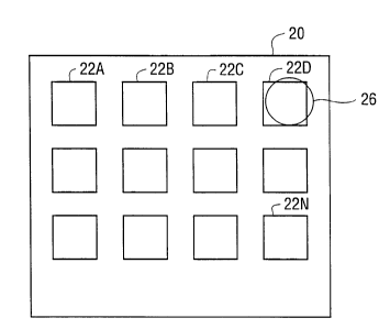
FIGURE 1 illustrates a cantilever palette constructed in accordance with an
embodiment of the invention.
FIGURE 2 illustrates individual cantilevers forming a portion of a cantilever
block of the cantilever palette of Figure 1.
FIGURE 3 illustrates a portion of a diffraction grating utilized in accordance
with an embodiment of the invention.
FIGURE 4 illustrates a cantilever with a force sensing material utilized in
accordance with an embodiment of the invention.
FIGURE 5 illustrates the deflection of the cantilever of Figure 4 in the
presence of a micro-force.
FIGURE 6 illustrates a diffraction grating utilized in accordance with an
embodiment of the invention.
FIGURES 7(a)-7(1) illustrate processing steps utilized to construct an
apparatus
in accordance with the invention.
FIGURE 8 illustrates image enhancement devices that may be used in
accordance with an embodiment of the invention.
FIGURE 9 illustrates a spatial filter with a 3 mm diameter clear aperture
which
allows first order signals to pass in accordance with an embodiment of the
invention.
FIGURE 10 illustrates a pin hole array utilized in accordance with an
embodiment of the invention.
Like reference numerals refer to corresponding parts throughout the drawings.
DETAILED DESCRIPTION OF THE INVENTION
Figure 1 illustrates a cantilever palette 20 constructed in accordance with an
embodiment of the invention. The cantilever palette 20 includes a set of
cantilever
array blocks 22A-22N. Each cantilever array block 22 includes a set of
cantilevers, as
shown in Figure 2, which illustrates a sub-set 26 of the cantilevers of
cantilever array
CA 02376325 2002-02-13
WO 01/14823 PCT/US00/22461
block 22D of Figure 1. Figure 2 illustrates individual cantilevers 28. Each
cantilever
28 includes cantilever fingers 30.
By way of example, the cantilever palette 20 contains N cantilever array
blocks
22, with each cantilever array block 22 being approximately 5 mm x 5 mm in
size,
thus individual array blocks 22 are visible to the naked eye and are
sufficiently large
for loading a substance that is to be sensed. In one implementation, each
cantilever
array block contains an array of approximately 50 x 50 cantilevers 28, with
each
cantilever 28 being about 100 ~m x 100 ~m in size. Each cantilever 28 may be
implemented with a series of 1-2 pm wide cantilever fingers 30.
Figure 3 illustrates a portion of a single cantilever 28 with cantilever
fingers
30. The cantilever 28 is surrounded by a substrate 40, which includes frame
fingers
41. The cantilever fingers 30 and the frame fingers 41 form a diffraction
grating 42.
As discussed below, in the presence of a predetermined force, the cantilever
28
deflects and the diffraction grating 42 produces observable diffracted light.
Figure 4 is a side view of a single cantilever 28. The cantilever 28 includes
a
force sensing material 50. The force sensing material 50 maybe an externally
applied
coating or it may be a material incorporated into the cantilever 28. The force
sensing
material is selected to sense chemical-mechanical, magnetic, electrostatic,
thermal
(conduction, convection, radiation), or other forces.
Figure 5 illustrates that in the presence of a predetermined micro-force, in
this
example illustrated as a substance 52, the interaction between the force
sensing
material 50 and the substance 52 causes the cantilever 28 to deflect. Incident
light 54
is diffracted by the deflected cantilever 28 through the diffraction grating
42 to
produce diffracted light 56, which is visually identifiable.
Figure 6 is a complete illustration of a single cantilever 28 constructed in
accordance with an embodiment of the invention. The cantilever 28 includes
cantilever fingers 30 surrounded by a substrate 40, which includes frame
fingers 41.
The combination of the cantilever fingers 30 and the frame fingers 41 forms a
diffraction grating 42.
Returning to Figure 1, the cantilever palette 20 may be configured in a number
of ways. For example, the cantilever palette may be configured such that each
cantilever array block 22 is used to sense a different micro-force. The micro-
forces
6
CA 02376325 2002-02-13
WO 01/14823 PCT/US00/22461
that may be sensed in accordance with the invention include chemical-
mechanical
forces, magnetic forces, electrostatic forces, thermal-mechanical
(thermomechanical)
forces, and the like. Typically, a cantilever palette 20 is configured to
sense a single
micro-force, for example a chemical-mechanical force induced by a
predetermined
substance. As used herein, the term substance refers to any liquid, gaseous,
or solid
matter.
Each cantilever array block 22 may be configured to be responsive to a
different predetermined substance. In this case, N different substances may be
sensed
with a single cantilever palette 20.
Alternately, each cantilever array block 22 may be configured to be responsive
to a predetermined level of a single substance. In such an embodiment, the
number of
blocks 22 producing visible light specifies the level of the sensed substance.
In another embodiment of the invention, the palette 20 is divided into
cantilever array block subsets. For example, a column of cantilever array
blocks 22
may be assigned to measure varying levels of a single substance. In this case,
the
number of cantilever array blocks 22 within a column that produces visible
light will
indicate the level of the sensed substance.
The foregoing aspects of the invention are more fully appreciated with
reference to a specific example. Consider the case where each of the N
cantilever
array blocks 22 is loaded with a single type of monoclonal antibody (Ab), such
that N
different types of antibodies are tested on a single palette 20. The
antibodies are
attached to one side of the cantilevers 28 in order to produce differential
surface stress.
When the cantilever palette 20 is exposed to a solution of antigens (Ag), the
high
specificity of the Ab-Ag reaction chemically and mechanically induces
deflection of
only the particular array of cantilevers that contains the corresponding
antibody. The
cantilevers deflect with respect to the surrounding stationary frame fingers
41. The
cantilever fingers 30 are designed such that the incidence of white light on
the array of
cantilever-based diffraction grating produces a predetermined color that is
visible to
the human eye.
Once the cantilever palette 20 is fabricated and loaded with antibodies, the
cantilever palette 20 is exposed to antigens and visually observed for color
change in
7
W~ 01/14823 CA 02376325 2002-02-13 pCT/US00/22461
the array. The cantilever palette 20 thereby operates as a micro-mechanical
"litmus
paper" for detection of antigens.
Observe that the cantilever palette 20 does not require external power, since
the
actuation is chemical and mechanical (chemical-mechanical) and the detection
is based
on dispersion of background white light. If necessary, a light source, such as
a light
emitting diode or a laser in conjunction with photodiodes can be used to
detect the
cantilever deflection. Another advantage of the invention is that a single 3
cm x 3 cm
chip can detect about (N=) 25-30 antigens making the process highly parallel.
The
low fabrication and operation costs for the cantilever palette 20 make it
disposable.
The high specificity of Ag-Ab reactions make the test highly selective. The
cantilever
palette is several orders of magnitude more sensitive than existing techniques
Advantageously, the cantilever palette is a "passive" device in the sense that
the
cantilevers are not oscillated, as commonly done with prior art cantilevers
used in
sensing applications. This visual output is achieved by the diffraction
grating
produced between the cantilever fingers 30 and the frame fingers 41. That is,
the
movement of the cantilever 28 causes the cantilever fingers 30 to move with
respect to
the stationary frame fingers 41, thereby producing an optically observable
event.
Since the output from the cantilever palette 20 is visually observable,
expensive
optical processing equipment is not required.
Monoclonal antibodies can be loaded into the cantilever palette 20 in several
ways. As known in the art, antibodies are proteins which tend to have higher
affinity
to glass than metal surfaces, such as gold. Hence, if one surface is coated
with gold
and the other with silicon dioxide, the antibodies preferentially cover more
of the glass
surface than the gold. Dipping the cantilever palette 20 into a solution of
antibodies is
sufficient for coating the glass-side of the cantilever with antibodies.
More sophisticated monoclonal antibody loading methods may also be used.
One method involves a mixed alkanethiol monolayer (self assembled monolayer or
SAM) which maintains a hydrophilic interface for the biomolecule, yet
passivates the
high energy gold surface from nonspecific adsorption. Covalent linkages
between the
biomolecule and the SAM are achieved via peptide linkages. Alternatively, if
the
silicon side of the cantilever (or an oxide coated metal surface) is to be
derivatized,
photodefinable silane monolayers may be used to couple biomolecules to the
surface.
8
CA 02376325 2002-02-13
WO 01/14823 PCT/US00/22461
It is important to avoid the standard silanes (e.g. trimethoxy derivatives)
because they
have a tendency to form three dimensional layers on the surface. This results
in loss of
coupling between the cantilever 28 and the added mass presented by the
antibody or
antibody/colloidal gold conjugate.
The cantilever 28 may be implemented with silicon nitride, polysilicon, and
single crystal silicon. Design parameters include size of the membrane, length
and
width of the cantilever, length and width of the cantilever fingers, the frame
fingers,
the number of fingers, and the like.
Figures 7(a)-7(1) illustrate processing steps that may be used to construct a
cantilever palette 20 in accordance with an embodiment of the invention.
Figure 7(a)
illustrates a semiconductor wafer 60 with 1 micron phosphosilicate glass (PSG)
layers
62. A plasma etch is used to pattern the backside of the wafer 60, resulting
in a
backside patterned PSG layer 64, as shown in Figure 7(b).
Next, the PSG layer on the top side is removed and the PSG layer on the back
side is thinned to 0.5 microns using plasma etching and a PSG wet etch. This
results
in the device of Figure 7(c). Figure 7(c) illustrates the wafer 60 with a
backside
patterned and thinned PSG layer 66.
A 0.5 micron PSG layer is then grown on both sides of the wafer 60. This
results in the device of Figure 7(d). Figure 7(d) illustrates the second PSG
layer 68. A
0.5 micron to 1.0 micron Low Pressure Chemical Vapor Deposition (LPCVD)
silicon
nitride layer is then grown onto the wafer 60, resulting in the structure of
Figure 7(e).
Figure 7(e) illustrates the resultant silicon nitride layers 70.
A silicon nitride cantilever is then patterned and etched using a plasma etch.
This results in the structure of Figure 7(f). Figure 7(f) is a side view of a
cantilever,
showing cantilever fingers 30 formed in a patterned nitride layer 72. Only one
cantilever is shown, but it should be appreciated that a batch process is
disclosed,
resulting in a large number of cantilevers, cantilever array blocks, and
cantilever
palettes being fabricated at the same time.
The next processing step relates to patterning deep alignment holes. Deep
alignment holes 74 are illustrated in Figure 7(g). The deep alignment holes 74
are
used to construct frames that will provide structural integrity for the
cantilevers. As
discussed above, the frames also include frame or frame fingers 41 which form
a
9
W~ 01/14823 CA 02376325 2002-02-13 pCT/US00/22461
portion of the diffraction grating. The frames are constructed by depositing a
thick
(e.g., 5-10 micron) polysilicon layer. Figure 7(h) illustrates a thick
polysilicon layer
76. A polysilicon frame is then patterned and etched, resulting in the device
of Figure
7(i). Figure 7(i) illustrates a PSG frame 78. A top view of the frame 78 would
illustrate frame fingers 41 positioned between the cantilever fingers 30.
The silicon nitride layer 70 on the backside of the wafer 60 is then plasma
etched, resulting in the device of Figure 7(j). The silicon nitride cantilever
is then
released using a wet etch. This results in the structure of Figure 7(k).
Observe in
Figure 7(k) that the cantilever and associated cantilever fingers 30 are
suspended.
The final processing step is to deep etch the silicon substrate 60. This
results
in the final device, as shown in Figure 7(1). The device can now function in
the
manner set forth above.
The invention has now been fully disclosed. Those skilled in the art will
recognize many variations of the invention that are within the general
teachings of the
invention. Further, those skilled in the art will appreciate that the
invention may be
exploited in connection with other physical devices. For example, the
invention need
not be used solely in connection with direct visual read out by a human eye.
The
images created in accordance with the invention may be applied to an imaging
device,
such as a charge coupled device and then be analyzed with image processing
software.
In addition, the invention may be used in connection with various image
enhancement
devices, such as beam sputters, lenses, and filters.
Figure 8 illustrate an image enhancement device in accordance with an
embodiment of the invention. The cantilever palette 20 projects an image
toward a
beam sputter 92, which also receives visible light from a low-power visible
light
source 90. The output from the beam splitter 92 is applied to a first visible
lens 94, a
spatial filter 96, a second visible lens 98, and then an imaging device, such
as a charge
coupled device 100. The output from the imaging device 100 is applied to an
image
processing system 102, which may include a standard computer executing
standard
image processing software.
As indicated above, incident light is diffracted by the diffraction grating.
In
particular, incident light is diffracted by the diffraction grating at a
series of specific
angles corresponding to the particular order of the diffraction. The first
focusing lens
w0 01/14823 CA 02376325 2002-02-13 PCTlUS00/22461
94 performs a spatial Fourier transform and generates the diffraction pattern
on its
focal plane. Because of the structure of the whole focal plane array, the
diffraction
pattern contains two different spatial frequencies: one corresponding to the
periodicity
of the inter-digital fingers (formed by the cantilever fingers and frame
fingers), and the
other corresponding to pixel-to-pixel periodicity within the cantilever array.
The
energy distribution between the diffraction orders depends on the relative
distance
between the movable and fixed inter-digital fingers. As shown in Figure 9, the
primary peaks in the diffraction pattern are determined by the high frequency
part
corresponding to the periodicity of the fingers, while low-frequency
periodicity of the
pixel provides the sub-order secondary peaks within the primary peaks. A
spatial filter
96 with a 3 mm diameter clear aperture allows first order signals to pass.
After the first order primary peak containing the sub-order peaks pass through
the spatial filter 96, a second lens 98 is used to perform an inverse Fourier
transport
and restores the wave-front from the spectral information. The aperture size
of the
spatial filter 96 is large enough to allow most of the sub-orders of the first
main order
to pass through. Thus, the wavefront still contains the cantilever array
information.
Variations on the structure of Figure 8 will be recognized by those skilled in
the art. For example, a subset of the components of Figure 8 may be used to
project
the image directly onto a human eye. In addition, an image enhancement
structure
may be attached directly to the cantilever palette 20. For example, as shown
in Figure
10, the cantilever palette 20 may be attached to a pin-hole array 112 via a
spacer 110.
The base of the pin-hole array 112 includes a dark mirror coating 114 with pin
holes
115 formed therein. Incident visible light 116 and scattered visible light 118
from the
cantilevers 28 pass through the pin holes 115. Each pin hole 115 is placed
directly
above the diffraction grating of each pixel in the array to reduce cross talk.
The pin hole array may be fabricated by depositing a coating of low
reflectivity
and transmissivity on a glass substrate and then patterning to leave 30 ~m
square
apertures. By placing the pin hole array 350 qm away from the cantilever
palette 20, it
was theoretically predicted and experimentally established, that the zeroth
order
intensity changed from bright to dark for a relative displacement of the
grating by 7~/4
(~,=632 nm was the He-Ne laser wavelength used here). Since the human eye can
11
W~ 01/14823 CA 02376325 2002-02-13 PCT/US00/22461
typically detect about 200 shades of gray scale, this results in a resolution
of about 1
nm for measuring cantilever deflections.
The foregoing description, for purposes of explanation, used specific
nomenclature to provide a thorough understanding of the invention. However, it
will
be apparent to one skilled in the art that the specific details are not
required in order to
practice the invention. In other instances, well known circuits and devices
are shown
in block diagram form in order to avoid unnecessary distraction from the
underlying
invention. Thus, the foregoing descriptions of specific embodiments of the
present
invention are presented for purposes of illustration and description. They are
not
intended to be exhaustive or to limit the invention to the precise forms
disclosed,
obviously many modifications and variations are possible in view of the above
teachings. The embodiments were chosen and described in order to best explain
the
principles of the invention and its practical applications, to thereby enable
others
skilled in the art to best utilize the invention and various embodiments with
various
modifications as are suited to the particular use contemplated. It is intended
that the
scope of the invention be defined by the following claims and their
equivalents.
12