Note: Descriptions are shown in the official language in which they were submitted.
CA 02376767 2001-12-07
WO 00/77923 PCT/US00/16208
TRANSISTOR AMPLIFIER HAVING REDUCED PARASITIC OSCILLATIONS
Background of the Invention
This invention relates generally to transistor
amplifiers and more particularly to transistor amplifiers
having reduced parasitic, or parametric, oscillations.
As is known in the art, transistor amplifiers,
particularly high power pHEMT and HBT power amplifiers,
frequently have oscillations that occur only when the
amplifier is driven by a large signal. Under small signal
conditions these oscillations are usually not present. Such
oscillations are sometimes referred to as parametric
oscillations since they depend on variations of particular
external parameters (bias, frequency, input drive, and
temperature). While the amplifier may appear perfectly
stable under small signal conditions, oscillations can
appear as the amplifier is driven harder. These
oscillations tend to be very sensitive to input drive, bias
conditions, and operating frequency. FIG. 1 shows a power
amplifier 10. The amplifier includes a plurality of
transistor devices 12 arranged as shown. Several typical
observated oscillations in such type of amplifier 10 are
shown in FIGS. 4 through 7. FIG. 4 shows subharmonic f/2
and 3f/2 oscillations. FIG. 5 shows a 200 MHz spurious
oscillation that appeared as an amplifier was driven about
0.5 dB into compression. FIGS. 6 and 7 show further
examples of troublesome spurious oscillations under power
drive. Additional examples may be found in "Power
Amplifiers: From Milliwatts to Kilowatts . . . Cool Devices
with Hot Performance, " Short Course Notes of Aryeh
Platzker's section, 1998 GaAs IC Symposium. Existence of
such oscillations can be a major problem in many wide band
radar applications, where the oscillation tones could be
CA 02376767 2001-12-07
WO 00/77923 PCT/US00/16208
mistaken for false signals. Elimination of these
oscillations is essential for the system to work properly.
One technique commonly used to reduce these
parasitic oscillations is to use a parallel R-C filter as
presented in "Power Amplifiers: From Milliwatts to Kilowatts
. . . Cool Devices with Hot Performance," Short Course
Notes Steve Nelson and Aryeh Platzker's section, 1998 GaAs
IC Symposium. Thus, referring to FIGS. 1 and 2, the
transistor devices 12 in FIG. 1 are replaced with the
transistor devices, such as transistor device 12' shown in
FIG. 2. Thus, here each device includes a plurality of
transistor cells 15, here each a FET, having the gate
electrodes G connected to a common node 16. A filter 18,
i.e., the R-C network, is connected between an input node 20
and the common node 16. These R-C filters (i.e., networks)
18 are generally placed on the gate manifold (i.e., the
common node 16) of the transistor cell 15, as shown in FIG.
2, is somewhat removed from the intrinsic transistor device.
As is also known in the art, drive dependent
oscillations were first studied in the 1920s and 30s for
tube amplifiers. Van Der Pol first studied how nonlinear
resistance can introduce forced oscillations. Reference is
made to " Forced Oscillations ina Circuit with Non-Linear
Resistance (Reception with reactive Triode)", by Balth Van
Der Pol, published by The London, Edinburgh, and Dublin
Philosophical Magazine and Journal of Science, series 7,
vol. III, no. 13, Jan 1927, pp. 65-81 and to Nonlinear
Oscillations, by Nicholas Minorsky, published by D. Van
Nostrand Company, Princeton, NJ 1962, page 241. Mandlestam
and Papalexi further investigated subharmonic oscillations
in electron tubes, as reported in Nonlinear Oscillations, by
Nicholas Minorsky, published by D. Van Nostrand Company,
Princeton, NJ 1962, page 469.
- 2 -
CA 02376767 2001-12-07
WO 00/77923 PCT/US00/16208
Over the years, numerous authors have investigated
the subject of large signal oscillations. See: Otward
Muller and William Figel, "Stability Problems in Transistor
Power Amplifiers," Proceedings of the IEEE, Aug. 1967, pp.
1458-1466; W. Mumford, "Some Notes on the History of
Parametric Oscillations," Proceedings of the IRE, May 1960,
pp 848-850; R. Phillips, "Parametric Oscillation in a Damped
Resonant System," IEEE Transactions on Circuit Theory,
December 1963, pp. 512-515; J. Manley and H. Rowe, "Some
General Properties of Nonlinear Elements - Part 1. General
Energy Relations," Proceedings of the IEEE, July 1956, pp.
904-913.
Subharmonic oscillations (f/2, 3f/2, etc.) have been
investigated in depth and many parallels to pumped varactor
diodes can be made to explain the phenomenon in pHEMT
devices. It is well known that a pumped varactor diode
gives rise to subharmonic components due to the nonlinear
capacitance. See also P. Penfield, Jr. & R. Rafuse,
Varactor Applications, The MIT Press, Cambridge, MA, 1962.
To first order, the gate of a FET can be analyzed as a
pumped varactor diode; a primary contributor to subharmonic
oscillations being the nonlinearity in Cgs and Cgd, where
Cgs is the gate to source capacitance and Cgd is the gate to
drain capacitance. See also J. Imbornone, M. Murphey, R.
Donahue, E. Heaney, "New Insight into Subharmonic
Oscillation Mode of GaAs Power Amplifiers Under Severe
Output Mismatch Condition," 1996 GaAs IC Symposium, pp. 307-
310. A simplified FET model is shown in FIG. 8 and its
equivalent input impedance is shown in FIG. 9, where:
G is the gate;
D is the drain;
S is the source;
IDS is the drain to source current;
- 3 -
CA 02376767 2001-12-07
WO 00/77923 PCT/USO0/16208
Rg is the gate resistance;
Cgs is the gate to source capacitance;
Cdg is the drain to gate capacitance; and
Cds is the drain to source capacitance.
Assuming the nonlinear capacitance, C(t), shown in
FIG. 3, varies as:
C(t) =Co+C2sin (2wat)
where t is time and the pumping frequency (input
drive frequency) is 2w0, oscillations will arise at half the
drive frequency provided
1Z1+Rs+ C2 W.
-7woCO Co
where 2coo is the input signal frequency, wo is the frequency
of the f/2 parasitic oscillation, Rs is the series
resistance of the diode (analogous to the gate resistance,
Rg), Z1 is the load impedance seen by the diode at w0
(analogous to the impedance looking back from the gate of
the FET), Co is the small signal capacitance, and C2 is the
nonlinear component of the varactor capacitance. Despite
the oversimplification of this theory, it qualitatively
describes the behavior of pHEMT power amplifiers.
Subharmonic oscillations will not appear under low drive (C2
--> 0), or if Rs is high enough. Adding the R-C filter 18
(FIG. 2) increases the input resistance enough at low
frequencies to eliminate oscillations under drive.
- 4 -
CA 02376767 2001-12-07
WO 00/77923 PCT/US00/16208
The subject of spurious parasitic oscillations has
been studied less, but is also due to nonlinearities in the
transistor. Some insight into spurious parasitic
oscillations may be found in the above-mentioned reference
by Otward Muller and William Figel. There the authors view
the amplifier as the superposition of a nonlinear amplifier
and a linear amplifier with the bias point determined by
input drive. The nonlinear amplifier causes subharmonic
oscillations while linear amplifier component causes
spurious oscillations. Driving the device hard results in a
negative input impedance which in turn can cause
oscillations. The resistance in the R-C filter 18 (FIG. 2)
offsets the negative resistance in the device, thereby
suppressing any oscillation.
Summary of the Invention
In accordance with one feature of the invention, a
transistor device is provided having a plurality of
transistor cells. Each one of the cells has a control
electrode for controlling a flow of carriers through a
semiconductor. The device has an input node. A plurality
of filters is provided. Each one of the filters is coupled
between the input node and a corresponding one of the
control electrodes of the plurality of transistor cells.
In one embodiment of the invention, pairs of the
control electrodes are connected to a common region and
wherein each one of the filters is coupled between the input
node and a corresponding one of the common regions.
In accordance with another feature of the invention,
the semiconductor provides a common active region for the
plurality of transistor cells.
In accordance with another feature of the invention,
each one of the filters comprises a resistor and a
capacitor, the resistor and the capacitor being connected in
- 5 -
CA 02376767 2009-01-21
78625-5
parallel between the input node and the corresponding one of
the control electrodes.
In accordance with another aspect of the
invention, there is provided a transistor device comprising:
a semiconductor; a plurality of transistor cells formed in
an active region of the semiconductor, each one of the cells
having a control electrode disposed between a pair of
regions and extending across the active region for
controlling a flow of carriers through the active regions
between the pair of regions; an input node; a plurality of
filters, each one of the filters being coupled between the
input node and a corresponding one of the control electrodes
of the plurality of transistor cells, each one of the
filters comprising: a conductive layer; a dielectric
disposed on the conductive layer; a resistive layer disposed
over the dielectric; a conductive electrode disposed in
electrical contact with a first portion of the resistive
layer and providing the input node; a connector in
electrical contact with a second portion of the resistive
layer, such second portion of the resistive layer being
displaced from the first portion of the resistive layer,
such connector passing through the dielectric and being in
electrical contact with the first conductor.
With such an arrangement, a compact resistor-
capacitor (R-C) network (i.e., R-C filter) is provided that
connects to pairs of control electrodes, e.g., gate fingers,
in each device. This compact R-C filter has successfully
eliminated parasitic oscillations in several monolithic
microwave integrated circuit (MMIC) power amplifiers. Due
to its compact size, it can be easily incorporated in
existing MMIC designs with little or no need for additional
tuning of the design. The compact R-C filter effectively
- 6 -
CA 02376767 2009-01-21
78625-5
eliminates drive dependent subharmonicc and spurious
oscillations in pHEMT power amlipfiers.
In accordance with another aspect of the
invention, there is also provided a transistor device
comprising: a semiconductor; a plurality of transistor
cells formed in an active region of the semiconductor, each
one of the cells having a control electrode disposed between
a pair of regions and extending across the active region for
controlling a flow of carriers through the active regions
between the pair of regions; an input node; a plurality of
filters, each one of the filters being coupled between the
input node and a corresponding one of the control electrodes
of the plurality of transistor cells, each one of the
filters comprising: a conductive layer; a dielectric layer
disposed on the conductive layer; a resistive layer disposed
over the dielectric; a conductive electrode disposed in
electrical contact with a first portion of the resistive
layer and providing the input node; a connector in
electrical contact with a second portion of the resistive
layer, such second portion of the resistive layer being
displaced from the first portion of the resistive layer,
such connector passing through the dielectric and being in
electrical contact with the conductive layer; and wherein
each one of the filters comprises: a resistor, such
resistor being provided by the resistive layer; and a
capacitor, such capacitor having as one plate thereof
portions of the conductive layer and as another plate
thereof portions of the resistive layer, portions of the
dielectric layer being disposed between the plates.
Brief Description of the Drawing
These and other features of the invention, as well
as the invention itself, will become more readily apparent
- 6a -
CA 02376767 2009-01-21
78625-5
from the following detailed description when taken together
with the following drawings, in which:
FIG. 1 is a schematic diagram of an amplifier
according to the PRIOR ART;
- 6b -
CA 02376767 2001-12-07
WO 00/77923 PCT/US00/16208
FIG. 2 is a schematic diagram of a transistor device
according to the PRIOR ART and adapted for use in the
amplifier of FIG. 1;
FIG. 3 is a schematic diagram of a transistor device
according to the invention and adapted for use in the
amplifier of FIG. 1;
FIG. 4 is a plot showing subharmonic parasitic
oscillation in the transistor devices used in the amplifier
of FIG. 1 when such devices are operated at a drain-gate
voltage (Vds) of 2 volts, a gate to source voltage (Vgs) of
-.562 volts, an input power Pin of 15.4 dBm and an input
frequency fo of 12 GHz;
FIG. 5 is a plot showing spurious parasitic
oscillation in the transistor devices used in the amplifier
of FIG. 1 when such devices are operated at a drain-gate
voltage (Vds) of 2 volts, a gate to source voltage (Vgs) of
-.507 volts, an input power Pin of 13.9 dBm and an input
frequency f0 of 12 GHz;
FIG. 6 is a plot showing spurious parasitic
oscillation in the transistor devices used in the amplifier
of FIG. 1 when such devices are operated at a drain-gate
voltage (Vds) of 2 volts, a gate to source voltage (Vgs) of
-.525 volts, an input power Pin of 13.9 dBm and an input
frequency fo of 9.5 GHz;
FIG. 7 is a plot showing spurious parasitic
oscillation in the transistor devices used in the amplifier
of FIG. 1 when such devices are operated at a drain-gate
voltage (Vds) of 2 volts, a gate to source voltage (Vgs) of
-.627 volts, an input power Pin of 13.9 dBm and an input
frequency fo of 9.5 GHz;
FIG. 8 is schematic diagram of a simplified FET
model equivalent circuit according to the PRIOR ART;
- 7 -
CA 02376767 2001-12-07
WO 00/77923 PCT/US00/16208
FIG. 9 is a schematic diagram of the effective input
impedance of the FET model of FIG. 8 according to the PRIOR
ART;
FIG. 10 is a diagrammatical plan view of the
transistor device of FIG. 3;
FIG. 11 is an exploded view of a portion of the
transistor device of FIG. 3, such exploded portion being
enclosed by the arrow labelled 9-9 in FIG. 10;
FIG. 12 is a diagrammatical cross-sectional view of
the portion of the transistor device of FIG. 11, such cross-
section being taken along line 10-10 in FIG. 11;
FIG. 12A is a schematic diagram of an R-C filter
used by the transistor device of FIG. 3;
FIG. 12B is diagrammatical cross-sectional view of
the portion of the transistor device of FIG. 11, such cross-
section being taken along line 10B-10B in FIG. 11;
FIG. 13 is an exploded view of a portion of the
transistor device of FIG. 10, such exploded portion being
enclosed by the arrow labelled 11-11 in FIG. 10; and
FIG. 14 is a diagrammatical cross-sectional view of
the portion of the transistor device of FIG. 13, such cross-
section being taken along line 12-12 in FIG. 13.
Description of the Preferred Embodiments
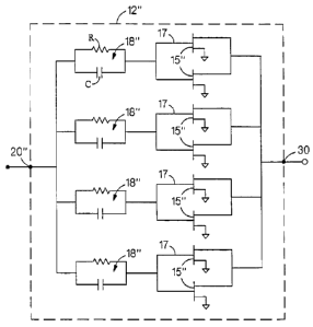
Referring now to FIG. 3, a transistor device 12" is
shown adapted for use in the amplifier of FIG. 1 in place of
the transistor device 12 used in such amplifier. The
transistor device 12" includes a plurality of transistor
cells, here eight cells 15". The cells 15" are formed in
the active region of a semiconductor, here for example, a
gallium arsenide semiconductor. Each one of the cells 15"
includes a control electrode 17, for example the gate
electrode where the cell is a FET, disposed between the
source and drain regions or the base electrode, where the
- 8 -
CA 02376767 2001-12-07
WO 00/77923 PCT/US00/16208
cell is a bipolar transistor, disposed between the emitter
and collector regions. Thus, with either the FET or bipolar
transistor the control electrode 17 (gate or base) controls
the flow of carriers in the active region between the a pair
of regions (source-drain or emitter-collector) in the active
region.
The transistor device 12" includes an input node
20". Each one of the control electrodes 17 is coupled to
the input node 20" through a R-C filter 18". Here, each
pair of the control electrodes 17 share one of the R-C
filter 18". Thus, here, in this example, there are four R-C
filters 18". Here, the transistor devices 15" are FETs with
source electrodes connected to ground and drain electrodes
connected to output node 30.
Referring now to FIGS. 10-14, the transistor device
12" is shown. The device 12" is formed on a semi-insulating
III-V, here gallium arsenide substrate 32 (FIGS. 12, 12B,
and 14). The device 12" includes the input node 20", the
plurality of, here eight, transistor cells 15", and the
plurality of, here four, R-C filters 18". Each one of the
cells 15" is formed in a common, mesa-shaped active region
34 (FIGS. 12, 12B, and 14) on the substrate 32. Each one of
the transistor cells 15" is here a FET having a finger-like
gate electrode 17 (i.e., control electrode) disposed between
a source region S, and a drain region, D. Thus, the gate
electrode 17 is used to control the flow of carriers between
the source S and drain D regions. Referring particularly to
FIGS. 13 and 14, it is noted that the source regions S are
in ohmic contact with source contacts and these are
electrically interconnected by an air-bridge conductor 40,
as shown most clearly in FIGS. 12, 12B, and 14. The source
regions S are connected to a ground plane conductor 43
- 9 -
CA 02376767 2001-12-07
WO 00/77923 PCT/US00/16208
disposed on the opposite surface of the substrate 32 as
shown most clearly in FIGS. 12B and 14.
Referring to FIGS. 10, 11, and 12, it is first noted
that each of the R-C filters 18" is identical in
construction. An exemplary one thereof is shown in detail
in FIGS. 11, 12, and 12B. Thus, such filter 18" includes a
conductive layer 40 disposed on the surface of the substrate
32. The conductive layer 40 is here gold. A dielectric
layer 42, here silicon nitride, is formed on the conductive
layer 40, as shown. A resistive layer 44, here tantalum, is
disposed over the dielectric layer 42. A conductive plate
or electrode 46, here gold, is disposed in electrical
contact with a first portion 50 of the resistive layer 44.
An electrical connector 52, here gold, is in electrical
contact with a second portion 54 of the resistive layer 44,
such second portion 54 of the resistive layer 44 being
displaced from the first portion 50 of the resistive layer
44. The distance between the portions 50, 52 of the
resistive layer 44 provides the resistor R of the R-C filter
18". The conductor layer 40 provides one plate, or
electrode of the capacitor C of the R-C filter 18", the
other plate of the capacitor C is provided by the conductive
plate 46 and the resistive layer 44. The dielectric of the
capacitor C is provided by the dielectric layer 42 disposed
between the resistive layer 44 and the plate 40. The
portion 54 of the resistive layer 44 is electrically
connected to: connector 52, as described; to the conductive
layer 40 by a conductive via 62 (FIG. 12) which passes
through the resistive layer 44 and the dielectric layer 42;
and, to an end of the control electrode 17 (FIG. 12B)
through the connector 52. Thus, the conductive via 62 (FIG.
12) electrically connects the portion 54 of the resistive
layer 44 to the lower plate of the capacitor C provided by
- 10 -
CA 02376767 2001-12-07
WO 00/77923 PCT/US00/16208
the conductive layer 40. The resulting R-C filter 18" is
shown in FIG. 12A. The plate 46 of the capacitor is
connected to input node 20" by an air-bridge conductor 47 as
shown in FIGS. 11, 12 and 12A. As noted above, each
one of the R-C filters 18" comprises a resistor R and a
capacitor C, the resistor R and the capacitor C being
connected in parallel between the input node 20" and the
corresponding one of the control electrodes 17 (FIGS. 12 and
12B). The resistive layer 44 serves both as the resistor
layer of the resistor R (here, for example, 6 ohms/sq) and
the top plate, or electrode of the capacitor, C. In order
to minimize the size of the R-c filter 18", the tantalum
resistive layer 44 layer serves both as the resistive layer
to provide the resistor R and as part of the upper plate or
electrode of the capacitor, C. At low frequencies, the
filter 18" sees only the resistor, R. In the operating
frequency band, however, the capacitor, C, begins to short
out the resistor, R, so that the gain is not degraded too
much.
We found a resistance of 10 ohms per pair of gate
fingers 17 to be adequate. The capacitance, C, was chosen
so that the capacitive reactance was equal to the resistance
at the low end of the band. For our case, using 1.67 pF per
pair of gate fingers 17 placed the 3 dB frequency of the R-C
at 9.5 GHz.
In a typical power amplifier, there will be 30 to 50
compact R-C filters in parallel as opposed to 4 to 8 filters
using the conventional approach. We believe the
conventional approach is less effective at eliminating
spurious oscillations as the size of the cell 12 increases
as compared to our invention. In order to assure stability,
performance of the conventional approach would degrade much
more than according to our invention.
- 11 -
CA 02376767 2001-12-07
WO 00/77923 PCT/US00/16208
Other embodiments are within the spirit and scope of
the appended claims. For example, while each filter 18" is
connected to a pair of control electrodes 17, a filter 18"
may be connected to only one control electrode 17 in which
case the device 12" in FIG. 3 would have 8 filters 18".
What is claimed is:
- 12 -