Note: Descriptions are shown in the official language in which they were submitted.
CA 02376885 2001-12-12
WO 00/77897 PCT/US00/13343
1
BURIED RIDGE SEMICONDUCTOR LASER WITH
ALUMINUM-FREE CONFINEMENT LAYER
1 O BACKGROUND OF THE INVENTION
1. Field of the Invention
The present invention relates generally to semiconductor lasers. In
particular, the
invention relates to a diode laser.
2. Technical Background
Semiconductor diode lasers emitting in the infrared portions of the spectrum
have
been sufficiently developed that they are widely used in a variety of
applications. In one
application, a high-power laser emitting, for example, at around 980nm,
optically pumps an
erbium-doped fiber amplifier (EDFA). It is known that such lasers can be
formed from
layers of, for example, GaInAs or AIGaAs or related materials grown on a GaAs
substrate.
For a typical edge-emitting laser, a p-n junction is formed by differential
doping of the
semiconductor layers, and electrical contacts are formed above and below the
junction to
provide the electrical power to forward bias the laser and thereby to
CA 02376885 2001-12-12
WO 00/77897 PCT/US00/13343
2
electrically pump it. Advanced structures include one or more very thin
undoped active
semiconductor regions formed into quantum wells between much thicker p-doped
and
n-doped semiconductor layers acting-both as optical cladding layers and
forming a
vertical p-n diode structure. Multiple quantum wells are electronically
isolated by barrier
layers. The composition and thickness of the quantum wells allow precise
tuning of the
emission wavelength, and hence the lasing wavelength. A horizontally extending
waveguide for the lasing radiation is formed by vertical and horizontal
optical
confinement structures. Mirrors, typically formed on the edges of the opto-
electronic
chip, define the ends of the laser cavity. The vertical optical confinement
structure is
usually closely associated with the p-n junction by appropriate compositional
profiles.
The horizontal confinement can be achieved by several structures, the two
which will be
discussed here being the etched ridge and the buried ridge.
In the etched ridge structure, the upper semiconductor cladding layer, which
for
example is a p-type layer, is selectively etched down close to but as far as
the active layer
to form a ridge in the upper cladding layer having a width of 2 to Spm, but
leaving a thin
portion of the upper cladding layer. The sides of the ridge are either exposed
to ambient
or covered with a material of low dielectric constant to thus provide a single-
mode
waveguiding structure. The ridge height is usually comparable to its width,
but it
effectively horizontally confines the light to a region mostly below the
ridge. One
electrical contact is made to the top of the ridge while typically the bottom
of the
substrate is electrically grounded for the other contact. The ridge provides
the additional
function of current confinement to guide the biasing current to a narrow
horizontal extent
of the underlying active layer corresponding to the ridge width so that
biasing current is
not wasted in areas outside of the waveguide.
The etched-ridge structure, however, suffers several problems when applied to
a
high power laser. The narrow width of the ridge and its upward projection from
the
substrate increases the series electrical resistance for the biasing current
and also
increases the thermal impedance for heat generated in the ridge. Furthermore,
etching of
CA 02376885 2001-12-12
WO 00/77897 PCT/US00/13343
the ridge is usually performed by diffusion-limited wet chemical etching
resulting in a
flared ridge, but the high power performance depends critically on the etching
profile of
the ridge. As a result, etched ridge lasers suffer poor reproducibility
The buried ridge structure avoids the projecting etched ridge and its
problems.
Instead, the growth of the upper semiconductor cladding layer, for example, of
p+-doped
AIGaAs, is divided into two portions. After a bottom portion of p+-doped
AI~Ga,_~As, is
deposited, a barrier or confinement layer of, for example, n+-doped AlbGa~_bAs
of higher
aluminum content (b>c) is grown on the lower portion of the AI~Ga,_~As, and a
hole is
patterned and etched down to the underlyingp+-doped AI~Ga~_~As layer. An upper
portion of the p+-doped AI~Ga~_~As cladding layer is then regrown both in the
hole over
the exposed p+-doped AI~Ga,_~As and over the top of the oppositely doped
AlbGa,_bAs
barrier layer. The opposite doping of the barrier layer confines the biasing
current to the
hole through the barrier layer. The upper portion of the upper cladding layer
within the
hole operates as a ridge extending upwardly from the lower portion. The
thickness of the
lower portion of the upper cladding layer is less than that needed to
vertically confine the
light, but the additional thickness of the ridge does confine it, both
vertically and
horizontally.
Typically, an n+-doped AIPGa~_PAs protective layer of lower aluminum content
(p<b) is grown on the Al6Ga,_bAs barrier layer prior to the hole etch in order
to prevent
the aluminum-rich barrier layer from being oxidized prior to regrowth.
However, the
protective layer does not protect the sidewall of the barrier layer after the
hole etching and
prior to the regrowth. Oxidation of the sidewall can lead to poor laser
reliability. In
general, to obtain a highly reliable laser, any aluminum-rich layer should be
avoided for
two reasons. Such a layer is subject to a higher degree of oxidation at any
cleaved facet.
Furthermore, it introduces tensile lattice strain relative to the aluminum-
lean layers since
the lattice constant of AIAs is less than that of GaAs.
It is thus desired to obtain a buried ridge laser that does not use an
aluminum-
containing barrier layer or other aluminum-containing layer exposed prior to
regrowth. It
CA 02376885 2001-12-12
WO 00/77897 PCT/US00/13343
4
is also desired to obtain a buried ridge laser that does not use an aluminum-
rich layer that
would be exposed during cleaving.
SUMMARY OF THE INVENTION
The invention includes a buried ridge semiconductor waveguide diode laser
based
on the AIGaAs family of materials. In one aspect of the invention, an aluminum-
free
confinement layer of opposite conductivity type from the upper AIGaAs cladding
layer is
deposited over the lower portion of the upper AIGaAs cladding layer and is
patterned
with a trench extending through the upper cladding layer to define both the
current
injection and the lateral optical confinement. A further layer of AIGaAs,
called an
uppermost cladding layer, is regrown in the aperture and over the confinement
layer. The
portion of the uppermost cladding layer in the trench extending through the
barrier layer
serves as a buried ridge to waveguide light. The confinement layer has the
composition,
for example, of GaInP.
In another aspect of the invention, an aluminum-free etch stop layer of, for
example, GaInAsP, is grown between the lower portion of upper cladding layer
and the
confinement layer. An etchant, for example a liquid such as HC1:H3P04 or
HCI:HBr:CH~COOH:H20, can be chosen which etches through the GaInP confinement
layer but stops on the GaInAsP. Thereby no aluminum-containing surface is
exposed for
the regrowth. The etchant preferably etches a V-shaped groove to form the
aperture in
the confinement layer.
BRIEF DESCRIPTION OF THE DRAWINGS
FIG. 1 is a cross-sectional view of one embodiment of a buried ridge laser of
the
invention.
FIG. 2 is a graph of the relationship between the lateral size of a first-
order optical
mode and the refractive contrast between the cladding and confinement layers.
FIG. 3 is a graph of the dependence of index contrast upon the thickness of
the
CA 02376885 2001-12-12
WO 00/77897 PCT/US00/13343
upper cladding layer.
DETAILED DESCRIPTION OF THE PREFERRED EMBODIMENTS
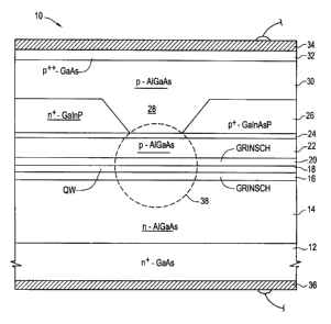
An embodiment of a diode waveguide laser 10 using an aluminum-free
confinement layer is illustrated in cross section in FIG. 1. A heterojunction
diode
structure is epitaxially grown on an n+-doped GaAs wafer 12 with a <001>
crystalline
orientation. The growth may be performed by molecular beam epitaxy (MBE) or
organo-
metallic chemical vapor deposition (OMCVD) among other methods. The diode
structure includes a lower, n-doped AIGaAs cladding layer 14 overlaid by a
lower graded-
index separate confinement heterostructure (GRINSCH) layer 16, an intrinsic
quantum
well structure 18, an upper GRINSCH layer 20, and a p-doped AIGaAs upper
cladding
layer 22. The optical emission wavelength ~,, corresponding to the lasing
wavelength, is
determined by the thickness of the one or more quantum wells in the quantum
well
structure 18 and their composition relative to thin electronic barrier layers
surrounding
and separating each quantum well. Exemplary compositions and thicknesses for
are a
single 6.Snm-thick quantum well of Gao,82lno_~gAs surrounded by 2nm-thick
barriers of
GaAs. The GRINSCH layers 16, 20 produce refractive indices linearly graded
between
the materials on either side so as to better optically confine the light, and
also have
compositional profiles producing an electric field promoting electron
transport through
the active quantum well structure 18. An exemplary GRINSCH layer 16, 20 has a
thickness of 170nm and a composition varying from Alo.osGao,9sAs to
Alo.ZgGao,72As.
This overall structure produces a beam with a far-field angle in the vertical
direction of
29° full-width, half-maximum.
In this embodiment, a thin (5 to l Onm) etch stop layer 24 of p-doped GalnAsP
is
grown over the upper cladding layer 22, and an aluminum-free confinement layer
26 of
n+-doped GaInP is grown over the stop layer 24. The composition of the
confinement
layer 26 is chosen relative to that of the upper cladding layer 22 such that
the confinement
layer 26 has a lower refractive index and a lateral refractive contrast Vin,
is formed
CA 02376885 2001-12-12
WO 00/77897 PCT/US00/13343
6
between the two materials. The confinement layer 26 is photomasked for a
buried ridge
extending along the <110> direction, which defines both the current injection
and the
lateral optical confinement. A sloped trench 28 is etched into the confinement
layer 26,
but the etching stops on the stop layer 24. This anisotropic etching can be
performed with
a wet etchant, such as HCl:H3P04 (1:1 by volume) or HCI:HBr:CH~COOH:H20
(30:30:30:5 by volume) which etches upwardly facing facets in GaInP but does
not etch
GaInAsP containing significant fractions of As.
The wafer is then returned to the growth chamber, and an uppermost cladding
layer 30 of p-doped AIGaAs, typically of the same composition and doping as
the upper
cladding layer 22, is regrown over the stop layer 24 at the bottom of the
trench 28 and
over the confinement layer 26. The AIGaAs filling the trench 28 acts as a
ridge
surrounded by the confinement layer 26 of lower refractive index. Because the
ridge acts
to laterally confine the optical wave in the layers mostly beneath it, the
depth of the
uppermost cladding layer 30 above the top of the confinement layer 26 is not
usually
crucial. It is possible to vary the composition and doping levels between the
upper and
the uppermost cladding layers 22, 30 for improved optical and electrical
effects.
However, they typically are formed of the same material.
A p++-doped GaAs contact layer 32 is grown over the uppermost cladding layer
30. Metal contact layers 34, 36 are deposited respectively on the front and
back of the
wafer to provide contact pads to the electrical biasing circuitry. The wafer
is then diced
into separate chips, and the chip's end faces are formed as mirrors defining
the ends of the
laser cavity, one of which is partially transmitting.
More precise compositions and thicknesses of the cladding and confinement
layers will now be presented as examples of the invention. However, these are
exemplary
only, and other parameters may be used with the invention. The cladding layers
14, 22 of
both conductivity types and the uppermost cladding layer 30 typically have
compositions
of A1o.28Gao.~~As for a laser designed to emit at 980nm. Because AIAs and GaAs
have
nearly the same lattice constants (0.56605 vs. 0.56533nm), the cladding layers
are
CA 02376885 2001-12-12
WO 00/77897 PCT/US00/13343
7
essentially lattice matched to the substrate 12. The composition of the
aluminum-free n+
confinement layer 26 is preferably chosen to be Gao.SiIno.49P, which is also
lattice
matched to GaAs. This composition produces a bandgap energy of 1.904eV, which
is
equal to that of Alo.~gSGao_6~SAs, and a refractive index of 3.268 at 980nm,
which is equal
to that of A1o.45Gaq,55As. The equality of bandgaps of the stop layer 24 and
the upper
cladding layer portions 22, 30 prevents the stop layer 24 from acting as a
barrier to
current injection. Because the confinement layer 26 has a conductivity type
opposite that
of the two upper cladding layer portions 22, 30, it confines the injection of
the biasing
current to the area of the buried ridge 28. However, the horizontal
confinement of the
current injection is restricted to the depth of the confinement layer 26, and
the trench
shape increases the average cross section. As a result, the series electrical
resistance is
minimized.
In view of the relative refractive indices between the confinement layer and
the
upper cladding layer, the aluminum-free GaInP confinement layer of the
invention can
provide similar horizontal optical confinement as the prior-art aluminum-rich
confinement layer. The combination of the vertical optical confinement
provided by the
cladding layers 14, 22, 30 and the GRINSCH layers 16, 18 and the horizontal
optical
confinement produced by the refractive contrast between the confinement layer
26 and
the upper cladding layers 22, 30 produces a waveguiding region 38 extending
along the
<O11> direction. The illustrated shape of the waveguiding region 38 is only
suggestive,
and indeed there is no sharp boundary for the guided wave.
To avoid the anti-guiding effect inducted by carrier injection, the lateral
index
contrast 0n, between the AIGaAs upper cladding layer 22 and the GaInP
confinement
layer 26 should be greater than Sx 10-3 for bulk lasers and greater than 1 x
10-3 for
quantum-well lasers. Further, it is generally desirable that the waveguiding
region 38
support only a single, fundamental mode, but that the lateral extent be
relatively large, for
example, Sp.m even for ~,=0.98~m so as to minimize optical power density on
the output
facet and thus eliminate any thermal damage of the facet. It is known that the
cutoff
CA 02376885 2001-12-12
WO 00/77897 PCT/US00/13343
8
width W~o for the first-order mode can be expressed primarily as a function of
the lateral
index contrast Vin, as
W
~~ 2 2n~~n~
where n is the average effective refractive index. At a waveguide width less
than the
cutoff width W~o, the waveguide supports only the fundamental mode so that the
structure
is single-moded, at least in the horizontal direction. As a result, the cutoff
width W~o
represents the maximum width of a single-mode waveguide. The relationship
between
the cutoff width W~o and the effective lateral refractive index contrast On,
is shown in the
graph of FIG. 2. A small value of 10-3 for On, is desired to increase the beam
size for
single-mode operation. The beam size is predominately determined by the width
of the
bottom of the trench 28 etched through the confinement layer 26.
However, other considerations need to be observed which result in a preferred
value of about 3x 10⁻³ for Vin,. The boundary between the confinement layer
and the
upper cladding layer, that is, the edge of the trench 28, defines both the
lateral
confinement of the optical field and the current injection confinement. With a
very low
index contrast, the optical field extends laterally far in the underlying
upper cladding
layer 22 beyond the edge of the confinement layer 26. As a result, the current
is injected
into only a portion of the waveguiding region. That is, the optical mode is
larger than the
gain region created by current injection. As a result, the optical gain or
efficiency is
degraded. For this reason, it is preferred that the index contrast Vin, be set
at about 3x 10-~
even for ridge widths of 5 to 7~m. The graph of FIG. 2 indicates that both a
fundamental
and a first-order lateral mode will be supported. However, operation with a
single lateral
mode can still be obtained as long as the fundamental mode enjoys sufficiently
higher
optical gain from the confined injected current. It is known that the first-
order mode is
less confined by the index discontinuities than is the fundamental mode for
index
contrasts On, of between 1 x 10⁻³ to 3x 10³ and ridge widths in the S to 7pm
range. Hence,
current confinement favors the fundamental mode.
CA 02376885 2001-12-12
WO 00/77897 PCT/US00/13343
9
The value of the effective index contrast On, depends in large part on the
thicknesses of the upper cladding layer 22 and of the confinement layer 24 as
well as on
their compositions. A model calculation produces the dependence of the index
contrast
0n, upon the thickness of the upper cladding layer 22 shown in the graph of
FIG. 3. A
thickness of 0.18um for the upper cladding layer 22 produces a index contrast
of 3 x 10-
for a far-field angle of 29-°°. Decreasing the far-field angle
to 22-°° increases the thickness
to 0.31 pin. The thicknesses would be about 50% larger for an etched ridge,
rather than
the buried ridge being discussed. Other model calculations show that index
contrast
significantly decreases for small thicknesses of the confinement layer 26,
that is, for
shorter ridges, but that the index contrast Oni saturates at about a thickness
of 0.4um for
the confinement layer 26. A slightly larger thickness is chosen.
In order to achieve a high kink power marking the transition from single-mode
to
mufti-mode operation, the p-type doping of the upper cladding layer needs to
be
optimized in order to match the carrier distribution the optical mode.
The lattice matching of the confinement layer to GaAs need not be precise. It
is
sufficient for lattice matching that the composition of the confinement layer
produces a
lattice constant equal to any combination of GaAs and AIAs.
Although it is preferred that the confinement layer 26 and the stop layer 24
be
completely free of aluminum, a small aluminum fraction, such as 2 atomic %
relative to
the anions, would still provide more than a factor of ten improvement for
oxidation
resistance over the prior art.
This laser design presented above produces optical emission at around 980nm.
The design can be extended to shorter wavelengths, even into the visible, by
increasing
the amount of aluminum in the AIGaAs cladding layers. However, to then obtain
the
higher refractive index in the confinement layer required to optically confine
the light to
the ridge, a substantial amount of aluminum may be added to the confinement
layer,
producing a composition GaAIInP. This aluminum fraction may be up to 10 to 15
atomic
% relative to the anions, but it is less than the aluminum fraction in the
AIGaAs cladding
CA 02376885 2001-12-12
WO 00/77897 PCT/US00/13343
5 layers and is substantially less than the aluminum fraction that would be
required in a
confinement layer not using GaInP as part of the confinement material.
Although the illustrated diode laser contained a quantum-well active region,
the
invention can be advantageously applied to bulk diode lasers in which a p-n
junction is
formed between the oppositely doped cladding layers, or a thin intrinsic
active layer may
10 be interposed to form a p-i-n junction.
The design of the invention offers many advantages over the prior art. The
buried
ridge structure offers much tighter control over the lateral index contrast
since it depends
only on the thicknesses and compositions of deposited layers. In contrast, the
etched
ridge structure produces a planar upper cladding layer having a thickness that
depends
upon the etching time for the ridge. Any variations in thickness uniformity or
etching
characteristics are magnified for the remaining upper cladding layer and its
thickness
effect upon the index contrast. The buried ridge structure also provides lower
series
electrical resistance than the etched ridge structure since the contact for
the buried ridge
structure can be made much larger than the width of the optical waveguide.
Furthermore,
thermal impedance is reduced for the buried ridge structure.
The buried ridge laser diode of the invention offers the advantage over the
prior-
art buried ridge laser diode that both the confinement layer and the stop-etch
layer are free
of aluminum or at least of reduced aluminum content. As a result, less or no
aluminum is
exposed during regrowth. The lack of opportunity for oxidation during the
regrowth
results in a more reliable device.
It will be apparent to those skilled in the art that various modifications and
variations can be made to the present invention without departing from the
spirit and
scope of the invention. Thus, it is intended that the present invention covers
the
modifications and variations of this invention provided they come within the
scope of the
appended claims and their equivalents.