Note: Descriptions are shown in the official language in which they were submitted.
CA 02377116 2002-03-18
FP01-0222-00
TITLE OF THE INVENTION
Optical Waveguide Module
BACKGROUND OF THE INVENTION
Field of the Invention
The present invention relates to an optical
waveguide module having a planar waveguide type of
optical waveguide formed on a substrate.
Related Background Art
In an optical circuit that makes use of an optical
waveguide., such as an optical fiber or planar optical
waveguide, it is sometimes desirable to control the
optical intensity of signal light to a suitable value,
such as by keeping the optical intensity constant for
signal light transmitted through optical waveguides.
In such a case, the optical intensity of the signal
light is monitored in the optical circuit, and
sometimes the optical intensity is also controlled on
the basis of the results of this monitoring.
SUMMARY OF THE INVENTION
This monitoring of the optical intensity~of signal
light used to be accomplished by providing an optical
coupler on an optical waveguide and splitting part of
the signal light. With this method, an optical coupler
is provided at a specific location along the optical
waveguide, a few percent of the signal light is split,
and the optical intensity of this split light is
1
CA 02377116 2002-03-18
FPOl-0222-00
monitored with a photodetector, which allows the
optical intensity of the signal light transmitted
through this optical waveguide to be monitored.
A problem with this use of an optical coupler,
though, is that it increases the number of optical
components that make up the optical circuit, and
furthermore, since these have to be fused together, the
structure and manufacturing process of the optical
circuit become more complicated.
In contrast, methods have been proposed in which
an optical coupler is not used, and instead part of the
signal light is reflected and the optical intensity
monitored. For instance, with the optical device
discussed in Japanese Patent Application Laid-Open H6-
15. 331837, an end face is formed at an angle with respect
to the optical axis at a specific location along an
optical waveguide, reflected light, part of the signal
light reflected from this end face in a direction
different from the optical axis, is detected, and the
optical intensity is monitored. Also, the optical
fiber discussed in Japanese Patent Application Laid-
Open 2000-155235 relates to a light splitting/merging
structure, in which an end face is formed perpendicular
to the optical axis at a specific location along an
optical fiber, part of the signal light is emitted
outside, and part of the emitted light is reflected and
2
CA 02377116 2002-03-18
FP01-0222-00
taken off by another end face that is inclined with
respect to the optical axis.
However, when part of the signal light is thus
reflected and used to monitor the optical intensity,
the reflectivity of the signal light at the inclined
end face varies with the state of polarization of the
signal light being reflected: Consequently, a problem
is that the optical intensity cannot be correctly
monitored unless the state of polarization of the
signal light transmitted through the optical waveguide
is specified. Also, the end face of the optical
waveguide can become contaminated if it is exposed to
the outside atmosphere, resulting in inferior long-term
stability of the reflectivity and so forth.
The present invention was conceived in an effort
to solve the above problems, and it is an object
thereof to provide an optical waveguide module with
which the structure of the optical circuit is simpler,
and the optical intensity can be correctly monitored
regardless of the state of polarization of the signal
light.
To achieve the stated object, the optical
waveguide module according to the present invention is
characterized by comprising (1) a planar waveguide
optical circuit, consisting of a substrate and a planar
waveguide type of optical waveguide formed on this
3
CA 02377116 2002-03-18
w
FP01-0222-00
substrate, and having a groove formed at a
predetermined inclination angle 8 (0° < 8) with respect
to the vertical axis perpendicular to the optical axis
of the optical waveguide so as to cross a specific area
of the optical waveguide, (2) a reflection filter that
is installed on the inside of the groove of the planar
waveguide optical circuit including a portion where
signal light transmitted through the optical waveguide
passes through, and that reflects part of the signal
light according to a specific reflectivity in which the
difference in reflectivity between the orthogonal
polarization has been compensated, (3) a filler resin
installed so as to seal at least the inside of the
groove, and (4) a photodetector that detects reflected
light of the signal light reflected by the reflection
filter.
With the above-mentioned optical waveguide module,
rather than the optical waveguide being split with an
optical coupler, of the signal light is reflected in an
inclined groove provided to the optical waveguide, and
the optical intensity of the signal light can be
monitored by means of this reflected light. As a
result, the structure and manufacturing process of the
optical circuit are simplified.
Also, rather than the reflection of the signal
light being performed on the end face of the groove, a
4
CA 02377116 2002-03-18
FPO1-0222-00
reflection filter that has undergone polarization
compensation for equalizing the reflectivity between
the polarization states is installed in the groove, and
part of the signal light is reflected by this
reflection filter and used to monitor optical intensity.
Here, since the reflectivity of the signal light by the
reflection filter becomes substantially constant
regardless of the polarization state of the signal
light transmitted through the optical waveguide, it is
possible to monitor the optical intensity accurately
regardless of the polarization state of the signal
light. Also, since the inside of the groove including
the reflection filter is sealed with a filler resin,
the end face of the groove and the reflection filter do
not come into contact with the outside atmosphere,
which prevents any deterioration in long-term stability
that would otherwise be caused by contamination of the
end face and so forth.
The present invention will be more fully
understood from the detailed description given
hereinbelow and the accompanying drawings, which are
given by way of illustration only and are not to be
considered as limiting the present invention.
Further scope of applicability of the present
invention will become apparent from the detailed
description given hereinafter: However, it should be
5
CA 02377116 2002-03-18
FP01-0222-00
understood that the detailed description and specific
examples, while indicating preferred embodiments of the
invention, are given by way of illustration only, since
various changes and modifications within the spirit and
scope of the invention will be apparent to those
skilled in the art from this detailed description.
BRIEF DESCRIPTION OF THE DRAWINGS
Fig. 1 is a plan view of the structure in a first
embodiment of the optical waveguide module
Fig. 2 is a cross section and detail enlargement
of the structure of the optical waveguide module shown
in Fig. 1, cut along the optical axis
Fig. 3 is a graph of the change in polarization
dependent loss when the inclination of the reflection
surface is varied with respect to the optical axis
along which the signal light is transmitted;
Figs. 4A to 4D are schematic views illustrating
the shape of the reflected light spot produced by the
reflection filter, and the shape of the light receiving
area of a photodetector;
Fig. 5 is a plan view of the structure in the
second embodiment of the optical waveguide module
Fig. 6 is a cross section and detail enlargement
of the structure of the optical waveguide module shown
in Fig. 5, cut along the optical axis
Fig. 7 is a plan view of the structure in the
6
CA 02377116 2002-03-18
FPO1-0222-00
third embodiment of the optical waveguide module;
Fig. 8 is a cross section and detail enlargement
of the structure of the optical waveguide module shown
in Fig. 7, cut along the I-I line;
Fig. 9 is a plan view of the structure in the
fourth embodiment of the optical waveguide module;
Fig. 10 is a cross section and detail enlargement
of the structure of the optical waveguide module shown
in Fig. 9, cut along the II-LI line;
Fig. 11 is a plan view of the structure in the
fifth embodiment of the optical waveguide modules and
Fig. 12 is a cross section and detail enlargement
of the structure of the optical waveguide module shown
in Fig. 11, cut along the III-III line.
DESCRIPTION OF THE PREFERRED EMBODIMENTS
Preferred embodiments of the optical waveguide
module according to the present invention will now be
described in detail through reference to the drawings.
Those elements that are the same will'be numbered the
same in the description of the drawings, and redundant
descriptions will be omitted. The scale in the
drawings does not necessarily coincide with that in the
description.
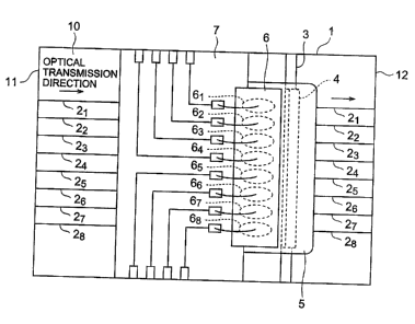
Fig. l is a plan view of the structure in a first
embodiment of the optical waveguide module according to
the present invention. This optical waveguide module
CA 02377116 2002-03-18
FP01-0222-00
comprises a planar waveguide optical circuit 1 having a
substrate 10 and eight (eight channels) planar
waveguide type of optical waveguides 21 to 28 formed on
the substrate 10.
The optical waveguides 21 to 28 are formed
parallel to each other and equidistantly, extending
from an input end 11 of the planar waveguide optical
circuit 1 to an output end 12 in a predetermined
optical transmission direction (the direction indicated
by the arrow in Fig. 1). A groove 3 that cuts across
the optical waveguides 21 to 28 is provided at a
specific location with respect to the optical
transmission direction of the planar waveguide optica l
circuit 1.
On the inside of this groove 3 is installed a
reflection filter 4 for reflecting part of the signal
light transmitted through the optical waveguides 21 to
2g respectively, with the reflection filter 4 being
sealed in the groove 3 by a filler resin 5. A sub-
mounting substrate 7 is installed above the planar
waveguide optical circuit 1 at a location further
upstream than the groove 3, and a photodetector array 6
having eight photodetectors 61 to 6g corresponding to
the optical waveguides 21 to 2$ is installed above the
filler resin 5 and the sub-mounting substrate 7. The
planar waveguide optical circuit 1 and the sub-mounting
8
CA 02377116 2002-03-18
FPO1-0222-00
substrate 7 are soldered together, for example, as are
the sub-mounting substrate 7 and the photodetector
array 6.
In Fig. l, the dotted lines indicate the shapes of
the light receiving areas of the photodetectors 61 to
68. The sub-mounting substrate 7 is a mounting member
for mounting the photodetector array 6, and on its top
surface are formed wiring, electrodes, etc., for
reading out the photodetection signals from the
photodetectors 61 to 68, as shown schematically in Fig.
1.
Fig. 2 is a cross section of the structure of the
optical waveguide module shown in Fig. l, cut along the
optical axis (the optical transmission direction of the
planar waveguide optical circuit 1) of the optical
waveguides 2n {n = 1 to 8). In Fig. 2, the portion
including the groove 3, reflection filter 4, and the
photodetector array 6 is shown enlarged.
As shown in Fig. 2, the optical waveguide 2n in
the planar waveguide optical circuit 1 comprises lower
cladding 22, a core 20, and upper cladding 21 formed on
the substrate 10. The groove 3 that cuts across the
optical waveguide 2h at a specific area.is formed at a
specific inclination angle~A (0° < 8) with respect to
the vertical axis (shown by the dotted line in Fig. 2)
perpendicular to the optical axis of the optical
9
CA 02377116 2002-03-18
FP01-0222-00
waveguide 2n (perpendicular to the substrate 10), to a
depth d including at least the area where the signal
light transmitted through the optical waveguide 2n
passes through, corresponding to the core 20. In this
embodiment, the depth d of the groove 3 is set to be
greater than the thickness of the optical waveguide 2n.
The reflection filter 4 is inserted on the inside
of the groove 3. The reflection filter 4 is installed
so as to include at least the area where the signal
light transmitted through the optical waveguide 2"
passes through, at substantially the same angle 8 as
the groove 3 with respect to the optical axis. This
reflection filter 4 preferably consists of a dielectric
multilayer film filter, and is designed such that part
of the signal light with a specific wavelength (within
the specified wavelength band) transmitted through the
optical waveguide 2~ is reflected at a predetermined
reflectivity.
Furthermore, the dielectric multilayer film filter
that constitutes this reflection filter 4 is formed so
that the difference in reflectivity is compensated for
between the orthogonal polarization when signal light
is reflected, and the signal light components in
various states of polarization are reflected at
substantially the same reflectivity. This setting of
the reflectivity with respect to the signal light.
CA 02377116 2002-03-18
FPO1-0222-00
components in various polarization states is
accomplished, for example, by varying the dielectric
materials of the respective layers that make up the
dielectric multilayer film filter, the combinations of
these material, the thickness of the respective layer
films, etc.
The inside of the groove 3, including the
reflection filter 4, is sealed with the filler resin 5.
The filler resin 5 used in this embodiment is composed
of an inner filler resin 51 that seals the inside of
the groove 3, and an upper filler resin 52 that seals a
specific portion of the top surface of the planar
waveguide optical circuit 1 including the upper part of
the groove 3. The inner filler resin 51 and upper
filler resin 52 are integrally formed using the same
resin material.
The photodetector array 6, which has
photodetectors 6n (n = 1 to 8) corresponding to the
optical waveguide 2n, is installed on the top side of
the sub-mounting substrate 7 and the upper filler resin
52 part of the filler resin 5. The photodetector array
6 is disposed such that the reflected light obtained
when part of the signal light transmitted through the
optical waveguide 2n is reflected by the reflection
filter 4 will be incident on the light receiving area
of the corresponding photodetector 6~. Because of the
11
CA 02377116 2002-03-18
r
FP01-0222-00
incident direction of the reflected light, it is
preferable for the photodetectors 6n to be a rear
incidence type of photodiode or the like.
With the above structure, when the signal light
transmitted through an optical waveguide 2~ is emitted
through an upstream end face 31 to the inner filler
resin 51 inside the groove 3, the reflection filter 4,
which is inclined with respect to the optical axis,
reflects part of this signal light diagonally above the
planar waveguide optical circuit 1 at a predetermined
reflectivity that has undergone polarization,
compensation so as to be equal with respect to
polarization states. The rest of the signal light
passes through the inner filler resin 51 and the
reflection filter.4, and is again incident on the
optical waveguide 2n via a downstream end face 32.
Meanwhile, the light reflected by the reflection
filter 4 is incident on the photodetector 6n via the
inner filler resin 51, the optical waveguide 2n, and
the upper filler resin 52. The optical intensity of
the signal light transmitted through the optical
waveguide 2n is monitored on the basis of. the optical
intensity of the reflected light detected by the
photodetector 6n.
With the optical waveguide module in this
embodiment, rather than the optical waveguide itself
12
CA 02377116 2002-03-18
FPO1-0222-00
being split by means of an optical coupler or other
such optical components, part of the signal light is
reflected in the inclined groove 3 provided so as to
cut across the respective optical waveguides 2n, and
used for monitoring the optical intensity. This
simplifies the structure of the optical circuit of an
optical waveguide module with which the optical
intensity can be monitored. Also, there is no need to
install extra optical components, fuse the optical
waveguides together, and so forth, so the manufacturing
process is similarly simplified.
The reflection of the signal Light is not
performed by the end faces 31 and 32 of the groove 3,
and instead part of the signal light is reflected by
the reflection filter 4, which has undergone
polarization compensation so that the reflectivity
between the orthogonal polarization will be
substantially equal. Here, since the reflectivity o.f '
the signal light produced by the reflection filter 4
becomes substantially constant regardless of the
polarization state of the signal light transmitted
through the optical waveguide 2~, the optical intensity
of the reflected light detected by the photodeteetor 6n
can be used to accurately monitor the optical intensity
regardless of the polarization state of the signal
light.
13
CA 02377116 2002-03-18
FP01-0222-00
Also, the inside of the groove 3 including the
reflection filter 4 is sealed by the filler resin 5.
Since the end faces 31 and 32 of the groove 3, the
reflection filter 4, and so forth do not come into
contact with the outside atmosphere; any deterioration
in long-term stability that would otherwise be caused
by contamination of these components is prevented.
It is preferable here if the inclination angle 8
of the groove 3 and the reflection filter 4 with
respect to the vertical axis is within an angle range
of 0° < 8 <_ 40°.
Fig. 3 shows the change in polarization dependent
loss (PDL) when we vary the inclination of the
reflection surface with respect to the optical axis
along which the signal light is transmitted. As shown
in this graph, the reflection characteristics with an
ordinary reflection surface are such that there is no
polarization dependence and PDL = 0 when the
inclination angle 8 with respect to the vertical axis
is 0° (when the signal light is reflected in the'
opposite direction). As the inclination angle 8
increases, so does the polarization dependence of
reflectivity, and there is a sharp increase in the PDL
value once 8 goes over 40°.
If 6 thus becomes larger and the PDL increases, it
becomes difficult for the reflection filter 4 to
14
CA 02377116 2002-03-18
a
FP01-0222-00
perform polarization compensation for the difference in
reflectivity. Specifically, with a structure in which
the inclination angle 8 is large, the PDL value is
large and varies sharply with 6,, so extremely stringent
numerical conditions are required for the refractive
index of the respective layer materials, the film
thickness, and so forth in the dielectric multilayer
film filter used to compensate for the difference in
reflectivity. Consequently, for practical purposes it
is difficult to design and produce the dielectric
multilayer film filter of the reflection filter 4 so
that the difference in reflectivity will be
sufficiently compensated for. In contrast, if the
inclination angle 6 is set to an angle range of 0° < 8
<_ 40°, then the difference in reflectivity can be
compensated for at an adequate precision at the
reflection filter 4.
It is preferable for the filler resin 5 to be
composed of a resin material having substantially the
same refractive index as the core 20 of the optical
waveguides 2n (such as within a margin of error of 1°s).
If the inner filler resin 51 is a resin material
having substantially the same refractive index as the
core 20, then unnecessary reflection will be minimized
when signal light is emitted from the optical
waveguides 2n to the inner filler resin 51 (see point
CA 02377116 2002-03-18
a
s
FPO1-0222-00
P1 in Fig. 2). Also, unnecessary reflection will be
minimized when the light reflected by the reflection
filter 4 is incident from the inner filler resin 51 to
the optical waveguides 2n (see point P2).
If the upper filler resin 52 is a resin material
having substantially the same refractive index as the
core 20, then unnecessary reflection will ba minimized
when the light reflected by the reflection filter 4 is
incident from the optical waveguide 2p to the upper
filler resin 52 (see point P3).
If unnecessary reflection occurs at the interfaces
of the optical waveguides 2h, the inner filler resin 51,
and the upper filler resin 52, the reflection
characteristics of these components will have
polarization dependence according to the respective
reflection angles thereof. Therefore, if reflection
occurs without the refractive index being matched
between these components, then even though polarization
compensation is performed for the difference in
reflectivity at the reflection filter 4, the optical
intensity of the reflected light detected by the
photodetector 6n will depend on the polarization state
of the signal light. In contrast, if the refractive
indexes are matched so as to minimize.unnecessary
reflection at the respective interfaces, it will be
possible to accurately monitor optical intensity
16
CA 02377116 2002-03-18
FPO1-0222-00
regardless of the polarization state of the signal
light.
When the upper filler resin 52 is provided in
addition to the inner filler resin 51 as in this
embodiment, it is preferable to use resin materials
having substantially the same refractive index for
these filler resins 51 and 52. This allows the
unnecessary reflection of signal light (reflected
light) at the interface of the inner filler resin 51,
as well as the unnecessary reflection of signal light
(reflected light) at the interface of the upper filler
resin 52 to be similarly controlled.
The filler resins 51 and 52 may also be formed
integrally, using the same resin material. This
simplifies the step of installing the resin. The
difference in refractive index between the core 20 and
the upper cladding 21 is usually small enough to be
ignored for the purposes of this reflection problem.
If a problem is posed by unnecessary reflection
when the light reflected by the reflection filter 4 is
incident from the upper filler resin 52 to a
photodetector 6h (see point P4), it is preferabla to
provide an antireflective coating at the interface
between the filler resin 5 and the photodetector
This minimizes the unnecessary reflection that occurs
when reflected light from the reflection filter 4 is
17
CA 02377116 2002-03-18
a
FP01-0222-00
incident on the photodetector 6n, and makes it possible
to accurately monitor optical intensity regardless of
the polarization state of the signal light, just as
with the unnecessary reflection at the above-mentioned
interfaces of the optical waveguides 2~, the inner
filler resin 51, and the upper filler resin 52.
As to the structure of the photodetectors 6" and
the photodetector array 6, as shown in Fig. 1, it is
preferable if the light receiving areas of the
photodetectors 6n are formed in a substantially
elliptical shape whose major axis lies in the direction
of the optical axis of the optical wavegui.des 2", and
whose minor axis lies in the direction in which the
optical waveguides 2~ are laid out.
' Fig. 4A to 4D are schematic views illustrating the
shape of~the.reflected light spot of the reflected
light produced by the reflection filter 4, and the
shape of the light receiving area of a photodetector 6n.
The signal light transmitted through an optical
- waveguide 2n has a substantially circular signal light
spot because of the shape of the core 20, etc.
Therefore, the reflected light produced when this
signal light is reflected by the inclined reflection
filter 4 (see the side view in Fig. 4A) forms an
elliptical reflected light spot at the light receiving
area of the photodetector 6n, as indicated by the
18
CA 02377116 2002-03-18
a
FP01-0222-00
dotted line A in the plan view of Fig. 4B.
On the other hand, if the light receiving areas of
the photodetectors 6,-, are formed in a substantially
elliptical shape corresponding to the elliptical shape
of the reflected light spot and encompassing this
reflected light spot, as indicated by the solid line B
in Fig. 4B, the reflected light can be detected at a
sufficiently high light receiving.efficiency. It is
also possible to use a lens or the like to focus the
elliptical reflected light before it is incident on the
photodetector, but this drives up the cost because it
entails more optical components. By contrast, if the
shape of the light receiving areas of the
photodetectors 6n is made elliptical to match the
reflected light spot, the structure of the optical
waveguide module will be simplified and the cost
reduced.
If the shape of the light receiving area is
circular, as indicated by the solid line C in Fig. 4C,
2,0 the efficiency at which the reflected light is received
will be the same as with a substantially elliptical
shape, but the light receiving area will be wider in
the direction in which the photodetectors are laid out,
and which corresponds to the vertical direction in Fig:
4C (see 61 to 6$ in Fig. 1) . Consequently, the
photodetectors cannot be brought together at as high a
19
CA 02377116 2002-03-18
w
FP01-0222-00
density or as small a layout pitch in the photodetector
array, which increases the surface area of the optical
circuit and drives up its cost.
By contrast, if the shape of the light receiving
area is substantially elliptical, the layout pitch of
the photodetectors can be kept to a minimum, affording
a more efficiency optical circuit configuration.
If the shape of the light receiving area is
rectangular, as indicated by the solid line D in Fig.
4D, the photodetectors can be grouped together at the
same layout pitch as with a substantially elliptical
shape, but this configuration results in an unnecessary
light receiving area portion that is not used to
receive the reflected light being produced at the
corners of the light receiving area. This light
receiving area portion becomes a source of noise with
respect to the photodetection signal, and therefore
results in a decrease in efficiency in reflected light
detection, such as a deterioration in S/N ratio or a
smaller effective dynamic range. The same problem is
encountered with the above-mentioned circular light
receiving area.
On the other hand, if the shape of the light
receiving area is substantially elliptical, this will
reduce the generation of noise and so forth from the
unnecessary light receiving area portion, allowing the
CA 02377116 2002-03-18
FPO1-0222-00
optical intensity to be monitored more efficiently.
Still, a light receiving area that is circular or
rectangular maybe used as dictated by the layout pitch,
detection efficiency, and so on required of an
individual optical waveguide module.
Specific examples will now be given for the
optical waveguide module according to the above
embodiment.
A first example will now be given. In this
example; the groove 3 was formed at an inclination
angle 8 of 30° and a width w of 25 um in the optical
axis direction. The reflection filter 4 inserted
inside the groove 3 was a polarization compensated
filter with a width of 11 ~zm and a 10~ reflectivity of
signal light. The filler resin 5 comprised the same
resin material for both the inner filler resin 51 and
the upper filler resin J52. The refractive index of the
resin material, an adhesive with adjusted refractive
index, was n = 1.47 at a wavelength band of 1.51 to
1.61 um. The photodetectors 6n were each an InGaAs-PIN
photodiode having an elliptical light receiving area
with a diameter of 0.3 mm in the major axis direction
and a diameter of 0.15 mm in the minor axis direction.
The photosensitivity of this photodiode alone was 1.1
A/W.
The optical intensity of signal light was
21
CA 02377116 2002-03-18
FP01-0222-00
monitored using an optical waveguide module configured
as above, whereupon the polarization dependence of
reflectivity at the reflection filter 4 was loo for S
polarization and 10.30 for P polarization, and the
polarization dependent loss (PDL) was sufficiently low
at 0.1 dB, which confirmed that it was possible to
monitor the optical intensity in a state in which
dependence on the polarization state of the signal
light has been sufficiently reduced.
The photosensitivity with respect to the incident
signal light was about 0.1 A/W. This indicates that
the optical intensity of the signal light component
reflected by the reflection filter ~ at a reflectivity
of loo was detected by the photodetectors 6ri at an
efficiency of close to 100. The insertion loss of the
groove 3 and the reflection filter 4 into the optical
waveguides 2n was about l.0 dB, including the loss
produced by reflection of the signal light by the
reflection filter 4, diffraction of the signal light
inside the groove 3, and so forth.
A second example will now be given. In this
example, the groove 3 was formed at an inclination
angle A of 10° and a width w of 25 pm in the optical
axis direction. The reflection filter 4 inserted
inside the groove 3 was a polarization compensated
filter with a width of 11 um and a 10~ reflectivity of
22
CA 02377116 2002-03-18
FPOl-0222-00
signal light. The filler resin 5 comprised the same
resin material for both the inner filler resin 51 and
the upper filler resin 52. The refractive index of the
resin material, an adhesive with adjusted refractive
index, was n = 1.47 at a wavelength band of 1.51 to
1.61 um. The photodetectors 6n were each a photodiode
having an elliptical light receiving area with a
diameter of 0.3 mm in the major axis direction and a
diameter of 0.15 mm in the minor axis direction. The
photosensitivity of this photodiode alone was 1.1 A/W.
In this example, an antireflective coating was
provided at the interface between the upper filler
resin 52 and the photodetectors 6~ in order to prevent
unnecessary reflection that would be produced if
reflected light were incident on the photodetectors 6n.
The optical intensity of signal light was
monitored using an optical waveguide module configured
as above, whereupon the polarization dependence of
reflectivity at the reflection filter 4 was 9.7~ fox S
polarization and 10s for P polarization, and the
polarization dependent loss (PDL) was sufficiently low
at 0.1 dB, which confirmed that it was possible to
monitor the optical intensity in a state in which
dependence on the polarization state of the signal
light has been sufficiently reduced.
The photosensitivity with respect to the incident
23
CA 02377116 2002-03-18
FPO1-0222-00
signal light was about 0.1 A/W. This indicates that
the optical intensity of the signal light component
reflected by the reflection filter 4 at a reflectivity
of 10~ was detected by the photodetectors 6~ at an
efficiency of close to 1000. The insertion loss of the
groove 3 and the reflection filter 4 into the optical
waveguides 2n was about 1.0 dB, including the loss
produced by reflection of the signal light by the
reflection filter 4, diffraction of the signal light
inside the groove 3, and so forth.
It can be seen from the first and seconds examples
given above that optical waveguide modules with the
above configurations make it possible to accurately
monitor optical intensity regardless of the
polarization state of the signal light.
Another embodiment of the optical waveguide module
according to the present invention will now be
described.
Fig. 5 is a plan view of the structure in the
second embodiment of the optical waveguide module.
Just as with the first embodiment, this optical
waveguide module comprises a planar waveguide optical
circuit l having a substrate 10 and eight (eight
channels) planar waveguide type of optical waveguides
21 to 28 formed on the substrate 10.
The optical waveguides 21 to 28 are formed
24
CA 02377116 2002-03-18
FPO1-0222-00
parallel to each other and equidistantly, extending
from an input end 1l of the planar waveguide optical
circuit 1 to an output end 12 in a predetermined
optical transmission direction (the direction indicated
by the arrow in Fig. 5). A groove 3 that cuts across
the optical waveguides 21 to 2$ is provided at a
specific location with respect to the optical
transmission direction of the planar waveguide optical
circuit 1.
On the inside of this groove 3 is installed a
reflection filter 4 for reflecting part of the signal
light transmitted through the respective optical
waveguides 2l to 28, with the reflection filter 4 being
sealed in the groove 3 by a filler resin 5. A
photodetector array 60 having eight photodetectors 611
to 618 corresponding to the optical waveguides 21 to 28
is installed above the planar waveguide optical circuit
1 at a location further upstream than the groove 3. In
Fig. 5, the dotted lines indicate the shapes of the
light receiving areas of the photodetectors 611 to 618.
Fig. 6 is a cross section of the structure of the
optical waveguide module shown in Fig. 5, cut along the
optical axis of the optical waveguides 2n (n = 1 to 8).
In Fig. 6, the portion including the groove 3, the
reflection filter 4, and the photodetector array 60 is
shown enlarged. In the configuration shown in Fig. 6,
CA 02377116 2002-03-18
r
FPO1-0222-00
the reflection filter 4, the groove 3, and the planar
waveguide optical circuit 1 including the optical
waveguides 2" comprising the lower cladding 22, the
core 20, and the upper cladding 21 are configured the
S same as in Fig. 2.
The inside of the groove 3, including the
reflection filter 4, is sealed with the filler resin 5.
The filler resin 5 used in this embodiment is composed
of only the inner filler resin S1 that seals the inside
of the groove 3.
The photodetector array 60, which has
photodetectors 61n (n = 1 to 8) corresponding to the
optical waveguide 2~" is installed on the top side of
the upper cladding 2l of the planar waveguide optical
circuit 1. The photodetector array 60 is disposed such
that the reflected light obtained when part of the
signal light transmitted through the optical waveguide
2n is reflected by the reflection filter 4 will be
incident on the light receiving area of the
corresponding photodetector 61n. Because of the
incident direction of the reflected light, it is
preferable for the photodetectors 61" to be a rear
incidence type of photodiode or the like. An
antireflective coating may also be provided at the
interface between the photodetectors 61" and the upper
cladding 21 of the optical waveguides 2".
26
CA 02377116 2002-03-18
FPOI-0222-00
With the above structure, when the signal light
transmitted through an optical waveguide 2~ is emitted
through the upstream end face 31 to the inner filler
resin 51 inside the groove 3, the reflection filter 4,
which is inclined with respect to the optical axis,
. reflects part of this signal light diagonally above the
planar waveguide optical circuit 1 at a specific
reflectivity that has undergone polarization
compensation so as to be equal with respect to
respective polarization states. The rest of the, signal
light passes through the inner filler resin 51 and the
reflection filter 4, and is again incident on the
optical waveguide 2~, via the downstream end face 32.
Meanwhile, the light reflected by the reflection
filter 4 is incident on the photodetector 61n via the
inner filler resin 51 and the optical waveguide 2".
The optical intensity of the signal light transmitted
through the optical waveguide 2n is monitored on the
basis of the optical intensity of the reflected light
detected by the photodetector 61n.
With the optical waveguide module in this
embodiment, just as with the first embodiment, part of
the signal light is reflected in the inclined groove 3
provided so as to cut across the respective optical
waveguides 2n, and used for monitoring the optical
intensity. This simplifies the structure of the
27
CA 02377116 2002-03-18
h
FPO1-0222-00
optical circuit of an optical waveguide module with
which the optical intensity can be monitored. Also,
there is no need to install extra optical components,
fuse the optical waveguides together, and so forth, so
the manufacturing process is similarly simplified.
Also, since part of the signal light is reflected
by the reflection filter 4, 'which has undergone
polarization compensation so that the reflectivity
between the orthogonal polarization will be
substantially equal, the optical intensity of the
reflected light detected by the photodetector 61n can
be used to accurately monitor the optical intensity
regardless of the polarization state of the signal
light. Further, since the inside of the groove 3
including the reflection filter 4 is sealed by the
filler resin 5, the end faces 31 and 32 of the groove 3,
the reflection filter 4, and so forth do not come into
contact with the outside atmosphere, any deterioration
in long-term stability that would otherwise be caused
by contamination of these components is prevented.
If, as in the above first and second embodiments,
the planar waveguide optical circuit l has N number (N
is a plurality; N = 8 in the above embodiments) of
opticah waveguides and the optical intensity is
monitored for N channels of signal light transmitted
through these respective optical waveguides, then N
28
CA 02377116 2002-03-18
FP01-0222-00
number of photodetectors are installed corresponding to
the respective optical waveguides. The N channels of
signal light reflected by the reflection filter will
propagate through the respective reflected light paths
and be detected by the corresponding photodetectors,
and as a result the optical intensity of each channel
of signal light will be monitored.
Here, the signal light from the optical waveguides
reflected by the reflection filter is detected by the
corresponding photodetectors, but in some cases light
scattering or reflection produced at various locations
of the device, the spreading of the transmitted light,
and so forth may cause part of the light to be incident
on photodetectors of other adjacent channels, resulting
in crosstalk. If crosstalk thus occurs between
'adjacent channels, the optical intensity of the signal
light of those channels cannot be monitored accurately.
There are a number of possible causes of crosstalk
between channels. For instance, with the structure
shown in Fig. 2 or 6, possible causes of crosstalk
include scattered reflection at the interface between
the filler resin 5 and the various parts of the planar
waveguide optical circuit 1, scattering caused by
defects at the top surface of the upper cladding 21,
etc., and reflected light and scattered light caused by
scattered reflection at the interface between the
29
CA 02377116 2002-03-18
FP01-0222-00
substrate 10 and the lower cladding 22.
The signal light transmitted through an optical
waveguide mainly propagates through the core, but part
of the signal light spreads out and also propagates
through the upper and lower cladding near the core. If
there is too much spreading of the signal light to the
cladding, the reflected light path from the reflection
filter to the photodetector can spread out excessively,
unnecessary scattered light can be generated within the
optical waveguide or elsewhere, and so on, all of which
can cause crosstalk.
This spreading of the signal light to the cladding
also occurs, for example, as a result of misalignment
of the optical fibers used for inputting the signal
light, connected to the input end of the planar
waveguide optical circuit, with respect to the optical
waveguides. Specifically, if an optical fiber is
connected at a location away .from the core of the
optical waveguide, the inputted signal light will
propagate through the cladding and other components
that do not have a waveguide structure.
In the second embodiment, in which this problem of
crosstalk between channels was handled by directly
installing the photodetector array 60 on the top side
of the planar waveguide optical circuit l, without
providing a sub-mounting substrate or the like, the
CA 02377116 2002-03-18
FP01-0222-00
reflected light path from the reflection filter 4 to
the photodetector 61" is shorter and the spreading of
reflected light can be reduced, as shown in Fig. 6.
Also reduced is the effect of scattered reflection or
scattering at the interface or on the inside of the
optical waveguides 2" or filler resin 5. Therefore,
crosstalk between the channels is suppressed.
Also, enhancing the confinement of the signal
light within the core 20 with respect to the signal
light transmitted through the optical waveguides 2n is
preferable in terms of preventing crosstalk in both the
first and second embodiments. In specific terms, the
refractive index differential ~n between the core 20
and the cladding 2l and 22 should be increased. This
decreases the spreading of the signal light trap mitted
through the core 20 into the cladding 21 and 22.
Because of the high refractive index of the core, an
effect of confining the light inside the core will also
be achieved for the signal light component that leaks
into the cladding due to misalignment of an optical
fiber, etc.
As an example, with the structure shown in Fig. 6,
when an optical fiber was connected in a state in which
the fiber was misaligned by being offset by 2 um from
the core of an optical waveguide with a core size of
8.5 pm square, and a refractive index differential ~n
31
CA 02377116 2002-03-18
FP01-0222-00
of 0.3o between the core 20 and the cladding 21 and 22,
crosstalk worsened to -22 dB. In contrast, when the
refractive index differential On was raised from 0.30
to 0.45$, crosstalk improved to a level of < -25 dB.
We will now describe a method for manufacturing a
planar waveguide optical circuit when the refractive
index differential 4n between the core and cladding is
thus increased. The core and the upper cladding
(overcladding) are formed, for example, by using an
Si02 (quartz) glass micropowder to which the respective
required additives have been added, depositing this
powder by flame hydrolysis deposition (FHD) method, and
sintering.
More specifically, the core can be germanium(Ge)-
added Si02 glass, and the upper cladding can be
boron/phosphorus(B/P)-added Si02 glass, for example.
The germanium, boron, phosphorus, arid Si02 are obtained
in the form of soot-like micropowders by hydrolyzing
GeCl4, BC13, POC13, and SiCl4, respectively, in an
oxyhydrogen burner. The refractive index differential
~n is adjusted by adjusting the amount of germanium
added to the core and the amounts of boron and
phosphorus added to the upper cladding.
For instance, the amount of germanium added to the
core is typically about 3.2 wt% Ge concentration when
~n = 0.3~, and about 4.6 wto Ge concentration when ~n
32
CA 02377116 2002-03-18
FPOI-0222-00
- 0.450. The amounts of boron and phosphorus added to
the upper cladding are determined by the Booting
conditions, etc., but are adjusted so that the amount
of added phosphorus, which increases the refractive
index, will be balanced with the amount of added boron,
which decreases the refractive index, and the
refractive index will be equivalent to that of pure
Si02 glass. The above method yields optical waveguides
with a refractive index differential ~n between the
core and the upper cladding of 0.3o and 0.45.
In addition to enhancing the effect of confining
the light within the core, providing a light path
isolation means between the light paths is also an
effective way to deal with the above-mentioned problem
of crosstalk between channels. Specifically, providing
light path isolation means between adjacent reflected
light paths almost completely prevents crosstalk from
occurring between adjacent channels. As a result, the
optical intensity of the N channels of signal light
transmitted through the respective optical waveguides
can be monitored more accurately.
Fig. 7 is a plan view of the structure in the
third embodiment of the optical waveguide module. Just
as with the first embodiment, this optical waveguide
module comprises a planar waveguide optical circuit 1
having a substrate 10 and eight (eight channels) planar
33
CA 02377116 2002-03-18
FP01-0222-00
waveguide type of optical waveguides 21 to 28 formed on
the substrate 10.
The optical wave guides 21 to 2a are formed
parallel to each other and equidistantly, extending
from an input end 11 of the planar waveguide optical
circuit 1 to an output end 12 in a predetermined
optical transmission direction (the direction indicated
by the arrow in Fig. 7). 1.~ groove 3 that cuts across
the optical waveguides 21 to 28 is provided at a
specific location with respect to the optical
transmission direction of the planar waveguide optical
circuit 1.
On the inside of this groove 3 is installed a
reflection filter 4 for reflecting part of the signal
light transmitted through the respective optical
waveguides 21 to 28, with the reflection filter 4 being
sealed in the groove 3 by a filler resin 5. A
photodetector array 62 having eight photodetectors 631
to 638 corresponding to the optical waveguides 21 to 28
is installed above the planar waveguide optical circuit
1 at a location further upstream than the groove 3.
In Fig. 7, one-dot chain lines indicate the
photodettector array 62 and the photodetectors 631 to
638 in order to illustrate the positional relationship
between the photodetector array 62 and the various
components; and to show the planar waveguide optical
34
CA 02377116 2002-03-18
FPO1-0222-00
circuit 1 in a state in which the photodeteetor array
62 has been removed.
In this embodiment, a light path isolation means
for isolating reflected light paths is provided within
the planar waveguide optical circuit 1 in between each
of the eight reflected light paths along which part of
the signal light transmitted through the eight channels
of optical waveguides 21 to 28 is reflected by the
reflection filter 4 to the corresponding photodetectors
631 to 638. This light path isolation means serves to
suppress the generation of crosstalk between adjacent
channels:
In specific terms, in this embodiment a light
blocking layer 25 is provided between each of the eight
optical waveguides 21 to 28 so as to block light from
passing from one reflected light path into an adjacent
reflected light path within the planar waveguide
optical circuit 1.
Specifically, light blocking layers 251, 252, 253,
259, 255; 256, and 257 are respectively provided between
the optical waveguides 21 and 22, between the optical
waveguides 22 and 23, between the optical waveguides 23
and 29, between the.optical waveguides 29 and 25,
between the optical waveguides 25 and 26, between the
optical waveguides 26 and 2~, and between the optical
waveguides 2-, and 28.
CA 02377116 2002-03-18
FP01-0222-00
Other than the above-mentioned light blocking
layers 251 to 25-, being provided to the planar
waveguide optical circuit 1, the structure of the
optical waveguide module in this third embodiment is
the same as that in the second embodiment shown in Figs.
5 and 6.
Fig. 8 is a cross section of the structure of the
optical waveguide module shown in Fig. 7, cut along the
I-I line perpendicular to the optical axis of the
optical waveguides 2n (n = 1 to 8). In Fig. 8, the
portion including the optical waveguides 23 to 25, the
light blocking layers 252 to 255, and the
photodetectors 633 to 635 is shown enlarged, with the
cross section passing through the centers of the
photodetectors 63~ to 635 (see cross section location B
indicated by the dotted line in Fig. 6).
As shown in Fig. 8, the planar waveguide optical
circuit 1 comprises the lower cladding 22 formed on the
substrate 10, eight cores 20 corresponding to the
optical waveguides 21 to 2$ formed in parallel and
equidistantly spaced on the lower cladding 22, and the
upper cladding 21 formed so as to cover all eight of
the cores 20 (the optical waveguides 21 to 28). The
photodetector array 62 including the photodetectors 631
to 638 is disposed above the upper cladding 21.
In this embodiment, the upper cladding 21 is
36
CA 02377116 2002-03-18
FP01-0222-00
removed from between the optical waveguides 21 to 28 in
specific widths of x1, and the light blocking layers
251 to 25-, for blocking light are provided in the
places where the upper cladding 21 has been removed.
As shown in Fig. 7, these light blocking layers 251 to
257 are formed over a specific length 11 spanning the
groove 3.
In the above structure, if we 'turn our attention
to the fourth channel of signal light transmitted
through optical waveguide 24, we see that when the
signal light transmitted through optical waveguide 29
is incident on the inner filler resin 51 in the groove
3 via the upstream end face 31 (see Fig. 6), the
reflection filter 4, which is inclined with respect to
the optical axis, reflects part of this signal light
diagonally above the planar waveguide optical circuit 1
at a specific reflectivity that has undergone
polarization compensation so as to be equal with
respect to respective polarization states. The rest of
the signal light passes through the inner filler resin
51 and the reflection filter 4, and is again incident
on the.optical waveguide 24 via the downstream end face
32.
Meanwhile, the light reflected :by the reflection
filter 4 is incident on the photodetector 634 via the
inner filler resin 51 and the optical waveguide 24.
37
CA 02377116 2002-03-18
FPOl-0222-00
The optical intensity of the fourth channel of signal
light transmitted through the optical waveguide 29 is
monitored on the basis of the optical intensity of the
reflected light detected by the photodetector 634.
The light blocking layer 253 is provided inside
the upper cladding 21 on the side with the optical
waveguide 23 and the photodetector 633, as viewed from
the optical waveguide 24. Of the signal light
transmitted through the optical waveguide 29, any light
that propagates to the adjacent photodetector 633 as a
result of light scattering or reflection, the spreading
of transmitted light, etc., is blocked by this light
blocking layer 253, and this prevents crosstalk between
the third and fourth channels.
Also; the light blocking layer 254 is provided
inside the upper cladding 21 on the side with the
optical waveguide 25 and the photodetector 635, as
viewed from the optical waveguide 29. Of the signal
light transmitted through the optical.waveguide 29; any
light that propagates to the adjacent photodetector 635
as a result of light scattering or reflection, the
spreading of transmitted light, etc., is blocked by
this light blocking layer 259, and this prevents
crosstalk between the fourth and fifth channels.
In this embodiment, light blocking layers 251 to
25~ are provided to the reflected light paths from the
38
CA 02377116 2002-03-18
FPO1-0222-00
reflection filter 4 to the photodetectors 631 to 638 as
light path isolation means for isolating the reflected
light paths from each other within the planar waveguide
optical circuit 1. As mentioned above, this
effectively prevents the generation of crosstalk
between adjacent channels.
It is preferable for the light blocking layers 251
to 257 provided within the planar waveguide optical
circuit 1 to be a light blocking material having the
effect of blocking light by absorbing, reflecting, or
scattering light of the signal light wavelength, or the
like. In specific terms, glass containing a high
concentration of an additive having a light absorption
effect, such as germanium, can be used, for example, as
the light blocking material.
As shown in Figs. 7 and .8, the light blocking
Layers 251 to 257 can be formed, for example, by a
method in which seven grooves, each with a.width of x1
and a length of 11, are formed substantially parallel
to the optical waveguides and spanning the groove 3
between the eight optical waveguides 21 to 28, and the
insides of these grooves are filled with a light
blocking material. The width x1 and length 11 of the
light blocking layers 251 to 257 are preferably set
such that the reflected light paths from the reflection
filter 4 to the photodetectors 63n are not too narrow,
39
CA 02377116 2002-03-18
FPO1-0222-00
and the light blocking effect can be sufficiently
realized between adjacent channels. Alternatively, a
light blocking layer can be provided over everything
from the input end 11 to the output end 12 of the
planar waveguide optical circuit 1.
As an example, in a state in which crosstalk has
worsened to =22 dB, providing a light blocking layer
within the upper cladding of the planar waveguide
optical circuit as discussed above improves the
crosstalk to a level of < -30 dB. Since the conduction
of scattered light will be somewhat suppressed even
when the inside of the light blocking layer is not
filled with anything, an improvement in crosstalk will
be obtained in this case as well, with the -22 dB
improving to -28 dB, for instance.
Fig. 9 is a plan view of the structure in the
fourth embodiment of the optical waveguide module.
Just as with the first embodiment, this optical
waveguide module comprises a planar waveguide optical
circuit 1 having a substrate 10 and eight (eight
channels) planar waveguide type of optical waveguides .
21 to 28 formed on the substrate 10.
The optical waveguides 21 to 28 are formed
parallel to each other and equidistantly, extending
from an input end 11 of the planar waveguide optical
circuit 1 to an output end 12 in a specific optical
CA 02377116 2002-03-18
r
FP01-0222-00
transmission direction (the direction indicated by the
arrow in Fig. 9). A groove 3 that cuts across the
optical waveguides 21 to 28 is provided at a specific
location with respect to the optical transmission
direction of the planar waveguide optical circuit 1.
On the inside of this groove 3 is installed a
reflection filter 4 for reflecting part of the signal
light transmitted through the respective optical
waveguides 21 to 28, with the reflection filter 4 being
sealed in the groove 3 by a filler resin 5. A sub-
mounting substrate 70 is installed above the planar
waveguide optical circuit 1 at a location further
upstream than the groove 3, and a photodetector array
64 having eight photodetectors 651 to 65$ corresponding
to the optical waveguides 21 to 2$ is installed above
the sub-mounting substrate 70 and the filler resin 5.
In Fig. 9, one-dot chain lines indicate the
photodetector array 64 and the photodetectors 651 to
65$ in order to illustrate the positional relationship
between. the photodetector array 64 and the various
components, and to show the planar waveguide optical
circuit l, the sub-mounting substrate 70, and so forth
in a state in which the photodetector array 64 has been
removed. The sub-mounting substrate 70 is a mounting
member for mounting the photodetector array 64, and on
its top surface are formed wiring, electrodes, etc.,
41
CA 02377116 2002-03-18
FP01-0222-00
for reading out the photodetection signals from the
photodetectors 651 to 658, as shown schematically in
Fig. 9.
In this embodiment, a light path isolation means
for isolating reflected light paths is provided within
the filler resin 5 in between each of the eight
reflected light paths along which part of the signal
light transmitted through the eight channels of optical
waveguides 21 to 28 is reflected by the reflection
filter 4 to the corresponding photodetectors 651 to 658.
This light path isolation means serves to suppress the
generation of crosstalk between adjacent channels.
In specific terms, in this embodiment the filler
resin 5 is installed so as to seal not only the inside
of the groove 3, but also a specific portion of the top
surface of the planar waveguide optical circuit 1
including the upper part of the groove. Light blocking
components 711 to 717 that protrude like the teeth of a
comb into the upper filler resin, which seals the top
surface of the planar waveguide optical circuit 1, are
provided to the sub-mounting substrate 70 located on
the upstream side of this upper filler resin.
Specifically, with respect to the optical
waveguides 21 through 28 located within the planar
waveguide optical circuit 1, light blocking components
711, 712, 713, 714, 715, 716, and 717 are respectively
42
CA 02377116 2002-03-18
t
FP01-0222-00
provided between the optical wavegu.ides 2l and 22,
between the optical waveguides 22 and 23, between the
optical waveguides 23 and 29, between the optical
waveguides 2Q and 25, between the optical waveguides 25
and 26, between the optical waveguides 26 and 27, and
between the optical waveguides 27 and 28.
Other than the above-mentioned light blocking
components 711 to 71-, being provided to the sub-
mounting substrate 70, the structure of the optical
waveguide module in this fourth embodiment is the same
as that in the first embodiment shown in Figs. 1 and 2.
Fig. 10 is a cross section of the structure of the
optical waveguide modals shown in Fp_g. 9, cut along the
II-II line perpendicular to the optical axis of the
optical waveguides 2n (n = 1 to 8). In Fig: 10, the
portion including the optical waveguides 23 to 25, the
light blocking components 712 to 715, and the
photodetectors 653 to 655 is shown enlarged, with the
cross section passing through the centers of the
photodetectors 653 to 655 (see cross section location A
indicated by the dotted line in Fig. 2).
As shown in Fig. 10, the planar waveguide optical
circuit 1 comprises the lower cladding 22 formed on the
substrate 10, eight cores 20 corresponding to the
optical waveguides 21 to 28 formed in parallel and
equidistantly spaced on the lower cladding 22, and the
43
CA 02377116 2002-03-18
FP01-0222-00
upper cladding 21 formed so as to cover all eight of
the cores 20 (the optical waveguides 21 to 28).
The upper filler resin 52, which is the portion of
the filler resin 5 that seals a specific portion of the
top surface of the planar waveguide optical circuit l,
is provided tb the top side of the upper cladding 21
(see Fig. 2). This upper filler resin 52 is
substantially the same height as the sub-mounting
substrate 70. The photodetector array 64 including the
photodetectors 651 to 658 is disposed above the upper
filler resin 52 and the sub-mounting substrate 70. The
portion under the photodetectors 65~, to 65$ of the
photodetector array 64 is the upper filler resin 52,
through which light from the reflection filter 4 is
able to pass.
In this embodiment, the comb-like light blocking
components 711 to 717, which are formed at a specific
width of x2 at the end faces of the sub-mounting
substrate 70 that come into contact with the upper
filler resin 52, are provided to the upper filler resin
52 at locations corresponding to between the optical
waveguides 21 to 28 (between the photodetectors 651 to
658). The light blocking components 711 to 717 are
designed to protrude into the upper filler resin 52,
which is downstream of the sub-mounting substrate 70.
These light blocking components 711 to 717 are formed
44
CA 02377116 2002-03-18
r.
FPO1-0222-00
over a specific length 12, as shown in Fig. 9.
Tn the above structure; if we turn our attention
to the fourth channel of signal light transmitted
through optical waveguide 24, we see that when the
signal light transmitted through optical waveguide 24
is incident on the inner filler resin 51 in the groove
3 via the upstream end face 31 (see Fig. 2), the
reflection filter 4, which is inclined with respect to
the optical axis, reflects part of this signal light
diagonally above the planar waveguide optical circuit 1
at a specific reflectivity that has undergone
polarization compensation so as to be equal with
respect to respective polarization states. The rest of
the signal light passes through the inner filler resin
51 and the reflection filter 4, and is again incident
on the optical waveguide 24 via the downstream end face
32.
Meanwhile, the light reflected by the reflection.
filter 4 is incident on the photodetector 654 via the
inner filler resin 51, the optical waveguide 24, and
the upper filler resin 52. The optical intensity of
the fourth channel of signal light transmitted through
the optical waveguide 24 is monitored on the basis of
the optical intensity of the reflected light detected
by the photodetector 654.
The light blocking component 713 is provided
CA 02377116 2002-03-18
FP01-0222-00.
inside the upper filler resin 52 on the side with the
optical waveguide 23 and the photodetector 653, as
viewed from the optical waveguide 24. Of the signal
light transmitted through the optical waveguide 24, any
light that propagates to the adjacent photodetector 653
as a result of light scattering or reflection, the
spreading of transmitted light, etc., is blocked by
this light blocking component 713, and this prevents
crosstalk between the third and fourth channels.
Also, the light blocking component 71g is provided
inside the upper filler resin 52 on the side with the
optical waveguide 25 and the photodetector 655, as
viewed from the optical waveguide 2~. Of the signal
light transmitted through the optical waveguide 24, any
light that propagates to the adjacent photodetector 655
as a result of light scattering or reflection, the
spreading of transmitted light, etc., is blocked: by
this light blocking component 714, and this prevents
crosstalk between the fourth and fifth channels.
In this embodiment, light blocking components 711
to 717 are provided to the reflected light paths from
the reflection filter 4 to the photodetectors 651 to
65$ inside the upper filler resin 52 of the filler
resin 5 as light path isolation means for isolating the
reflected light paths from each other. As mentioned
above, this effectively prevents the generation of
46
CA 02377116 2002-03-18
FPO1-0222-00
crosstalk between adjacent channels.
It is preferable for the light blocking components
711 to 717 provided to the sub-mounting substrate 70 so
as to protrude into the filler resin 5 to be a light
blocking material having the effect of blocking light
by absorbing, reflecting, or scattering light of the
signal light wavelength, or the like. In specific
terms, alumina can be used, for example, as the light
blocking material.
When the light blocking components ?11 to 717 are
formed integrally with the sub-mounting substrate 70 as
mentioned above, the sub-mounting substrate 70 itself
is formed from a light blocking material, for example.
The width x2 and length 12 of the light blocking
components 711 to 717 are preferably set such that the
reflected light paths from the reflection filter 4 to
the photodetectors 65h are not too narrow, and the
light blocking effect can be sufficiently realized
between adjacent channels.
As an example, in a state in which crosstalk has
worsened to -22 dB, providing light blocking components
within the upper filler resin of the filler resin as
discussed above improves the crosstalk to a level of <
-23 dB.
Fig. 11 is a plan view of the structure in the
fifth embodiment of the optical caaveguide module. Just
47
CA 02377116 2002-03-18
s
FP01-0222-00
as with the first embodiment, this optical waveguide
module comprises a planar waveguide optical circuit 1
having a substrate 10 and eight (eight channels) planar
waveguide type of optical waveguides 21 to 28 formed on
the substrate 10.
The optical waveguides 2l to 28 are formed
parallel to each other and equidistantly, extending
from an input end 1l of the planar waveguide optical
circuit l to an output end 12 in a specific optical
transmission direction (the direction indicated by the
arrow in Fig. 11). A groove 3 that cuts across the
optical waveguides 21 to 28 is provided at a specific
location with respect to the optical transmission
direction of the planar waveguide optical circuit 1.
On the inside of this groove 3 is installed a
reflection filter 4 for reflecting part of the signal
light transmitted through the respective optical
waveguides 21 to 28, with the reflection filter 4 being
sealed in the groove 3 by a filler resin 5. A sub-
mounting substrate 72 is installed above the planar
waveguide optical circuit 1 at a location further
upstream than the groove 3, and a photodetector array
66 having eight photodetectors 671 to 67$ corresponding
to the optical waveguides 21 to 28 is installed above
the sub-mounting substrate 72 and the filler resin 5.
In Fig. 11, one-dot chain lines indicate the
48
CA 02377116 2002-03-18
FP01-0222-00
photodetector array 66 and the photodetectors 671 to
678 in order to illustrate the positional relationship
between the photodetector array 66 and the various
components, and to show the planar waveguide optical
circuit 1, the sub-mounting substrate 72, and so forth
in a state in which the photodetector array 66 has been
removed. The sub-mounting substrate 72 is a mounting
member for mounting the photodetector array 66, and on
its top surface are formed wiring, electrodes, etc.,
for reading out the photodetection signals from the
photodetectors 671 to 678, as shown schematically in
Fig. 11 .
In this embodiment, a light path isolation means
for isolating reflected light paths is provided within
the planar waveguide optical circuit 1 in between each
of the eight reflected light paths along which part of
the signal light transmitted through the eight channels
of optical waveguides 21 to 28 is reflected by the
reflection filter 4 to the corresponding photodetectors
671 to 678. This light path isolation means serves to
suppress the generation of crosstalk between adjacent
channels.
In specific terms, in this embodiment a light
blocking layer 26 is provided between each of the eight
optical waveguides 21 to 28 so as to block light from
passing from one reflected light path into an adjacent
49
CA 02377116 2002-03-18
s
FPO1-0222-00
reflected light path within the planar waveguide
optical circuit 1.
Specifically, light blocking layers 261, 262, 263,
269, 265, 266, and 267 are respectively provided between
the optical waveguides 2z and 22, between the optical
waveguides 22 and 23, between the optical waveguides 23
and 24, between the optical waveguides 29 and 25,
between the optical wavegu.ides 25 and 26, between the
optical waveguides 26 and 27, and between the optical
waveguides 27 and 28.
Other than the above-mentioned light blocking
layers 261 to 267 being provided to the planar
waveguide optical circuit 1, the structure of the
optical waveguide module in this fifth embodiment is
the same as that in the first embodiment shown in Figs.
1 and 2.
Fig. 12 is a cross section of the structure of the
optical waveguide module shown in Fig. 11, cut along
the III-III line perpendicular to the optical axis of
the optical waveguides 2" (n = 1 to 8). In Fig: 12,
the portion including the optical waveguides 23 to 25,
the light blocking layers 262 to 265, and the
photodetectors 673 to 675 is shown enlarged, with the
cross section passing through the centers of the
photodetectors 673 to 675 (see cross section location A
indicated by the dotted line in Fig. 2).
CA 02377116 2002-03-18
FP01-0222-00
As shown in Fig. 12, the planar waveguide optical
circuit l comprises the lower cladding 22 formed on the
substrate 10, eight cores 20 corresponding to the
optical waveguides 21 to 28 formed in parallel and
equidistantly spaced on the lower cladding 22, and the
upper cladding 21 formed so as to cover all eight of
the cores 20 (the optical waveguides 21 to 28).
The upper filler resin. 52, which is the portion of
the filler resin 5 that seals a specific portion of the
top surface of the planar waveguide optical circuit 1,
is provided to the top side of the upper cladding 21
(see Fig. 2). This upper filler resin 52 is
substantially the same height as the sub-mounting
substrate 72. The photodetector array 66 including the
phatodetectors 671 to 67~ is disposed above the upper
filler resin 52 and the sub-mounting substrate 72. The
portion under the photodetectors 671 to 678 of the
photodetector array 66 is the upper filler resin 52,
through which light from the reflection filter 4 is
able to pass. .
In this embodiment, the upper cladding 21 i:s
removed from between the optical waveguides 21 to 2g in
specific widths of x3, and the light blocking layers
261 to 267 are provided in the places where the upper
cladding 21 has been removed. As shown in Fig. 11,
these light blocking layers 261 to 267 are formed over
51
CA 02377116 2002-03-18
FP01-0222-00
a specific length 13 spanning the groove 3.
in the above structure, if we turn our attention
to the fourth channel of signal light transmitted
through optical waveguide 29, we see that when the
signal light transmitted through optical waveguide 24
is incident on the inner filler resin 51 in the groove
3 via the upstream end face 31 (see Fig. 2), the
reflection filter 4, which is inclined with respect to
the optical axis, reflects part of this signal light
diagonally above the planar waveguide optical circuit 1
at a specific reflectivity that has undergone
polarization compensation sa as to be equal with
respectto respective polarization states. The rest of
the signal light passes through the inner filler resin
51 and the reflection filter 4, and is again incident
on the optical waveguide 2q via the downstream end face
32.
Meanwhile, the light reflected by the reflection
filter 4 is incident on the photodetector 674 via the
inner filler resin 51, the optical waveguide 24, and
the upper filler resin 52. The optical intensity of
the fourth channel of signal light transmitted through
the optical waveguide 24 is monitored on the basis of
the optical intensity of the reflected light detected
by the photodetector 674.
The light blocking layer 263 is provided inside
52
CA 02377116 2002-03-18
FP01-0222-00
the upper cladding 21 on the side with the optical
waveguide 23 and the photodetector 673, as viewed from
the optical waveguide 24. Of the signal light
transmitted through the optical waveguide 24, any light
that propagates to the adjacent photodetector 673 as a
result of light scattering or reflection, the spreading
of transmitted light, etc., is blocked by this light
blocking layer 263, and this prevents crosstalk between
the third and fourth channels.
Also, the light blocking layer 264 is provided
inside the upper cladding 21 on the side with the
optical waveguide 25 and the photodetector 675, as
viewed from the optical waveguide 24. Of the signal
light transmitted through the optical waveguide 24, any
light that propagates to the adjacent photodetector 675
as a result of light scattering or reflection, the
spreading of transmitted light, etc., is blocked by
this light blocking layer 264, and this prevents
crosstalk between the fourth and fifth channels.
In this embodiment, just as the light blocking
layers 251 to 257 in the third embodiment shown in Figs.
7 and 8, light blocking layers 261 to 26~ are provided
to the reflected light paths from the reflection filter
4 to the photodetectors 671 to 678 as light path
isolation means for isolating the reflected light paths
from each other within the planar waveguide optical
53
CA 02377116 2002-03-18
a
FPOl-0222-00
circuit 1. As mentioned above, this effectively
prevents the generation of crosstalk between adjacent
channels.
With this structure, in which the upper filler
resin 52 is provided by filling the space between the
photodetector array 66 and the upper cladding 21 of the
optical waveguides 21 to 2g with a resin, even if bumps
or the like are on the surface of the upper cladding 21,
any light scattering or scattered reflection caused by
these is suppressed:
As an example, in a state in which crosstalk has
worsened to -20 dB, providing a light blocking layer
within the upper cladding of the planar waveguide
optical circuit as discussed above improves the
crosstalk to a level of < -28 dB.
The optical waveguide moduiev of the present
invention is not limited to the embodiments and
examples given above, amd a variety ~f variations is
possible. For instance, the polarization compensation
of the difference in reflectivity at the reflection
filter 4 involves compensating for the difference in
reflectivity at the reflection filter 4 itself, but if
it is known in advance that polarization dependence
will be caused by reflection, etc., at the interfaces
of the optical waveguides 2~, the filler resin 5, and
the photodetectors 6n, the reflection filter 4 may also
54
CA 02377116 2002-03-18
FPO1-0222-00
be constituted with reflectivity that compensates for
these as well.
Also; the light path isolation-means for
preventing crosstalk between adjacent channels is not
limited to the structure discussed above, and various
other structures may be employed instead. For example,
when a light blocking member is provided inside the
filler resin, it may be a separate member from the sub-
mounting substrate, or a light blocking member may be
provided inside the inner filler resin: Alternatively,
a light blocking member provided inside the upper
cladding may be used together with a Light blocking
member provided inside the filler resin, for instance,
thereby further reducing crosstalk.
As described in detail above, the optical
waveguide module according to the present invention
offers the following effects. With an optical
waveguide module structured for use .in monitoring
optical intensity, in which an inclined groove is
formed cutting across optical waveguides and part of
the signal light is reflected by a reflection filter
installed inside this groove, the structure and
manufacturing process of the optical circuit are
simplified. Also, using a reflection filter that has
undergone polarization compensation so that the
reflectivity is equalized between orthogonal
CA 02377116 2002-03-18
FP01-0222-00
polarization makes it possible to monitor optical
intensity accurately regardless of the polarization
state of the signal light. Further, since the inside
of the groove including the reflection filter is sealed
with a filler resin, any deterioration in long-term
stability that would otherwise be caused by
contamination of these components is prevented.
An optical waveguide module such as this can be
used as a signal light intensity monitor that is
inserted into an optical circuit consisting of optical
fibers or planar optical waveguides. Alternatively, if
this optical waveguide module is provided at the
required location in a planar waveguide optical circuit
of a optical coupler, optical splitter, optical
attenuator, or the like, it will be able to monitor the
signal light intensity in the optical circuit.
Also, crosstalk can be minimized between adjacent
channels by providing light path isolation means
between N number of adjacent reflected light paths
through which N channels of signal light reflected by
the reflection filter propagate to photodetectors.
This makes it possible to accurately monitor the
optical intensity in each channel for N channels of
signal light transmitted through the respective optical
waveguides.
From the invention thus described, it will be
56
CA 02377116 2002-03-18
FPO1-0222-00
obvious that the invention may be varied in many ways.
Such variations are not to be regarded as a departure
from the spirit and scope of the invention, and all
such modifications as would be obvious to one skilled
in the art are intended for inclusion within the scope
of the following claims.
57