Note: Descriptions are shown in the official language in which they were submitted.
CA 02377166 2001-12-12
WO 01/01553 PCT/US00/17272
-1-
DYNAMICALLY-SWITCHED POWER CONVERTER
Field of the Invention
The present invention relates to DC/DC power supply controllers, and more
particularly to regulated capacitive-only or capacitive/inductive power
converters for
integrated power management systems.
Background of the Invention
Advances in electronics technology have enabled the design and cost-effective
fabrication of portable electronic devices. Thus, usage of portable electronic
devices
continues to increase as do the number and types of products. Examples of the
broad
spectrum of portable electronic devices include pagers, cellular telephones,
music players,
calculators, laptop computers, and personal digital assistants, as well as
others.
The electronics in a portable electronic device generally require direct
current
(DC) electrical power. Typically, one or more batteries are used as an energy
source to
provide this DC electrical power. Ideally, the energy source, such as consumer
batteries
of standard sizes such as AAA, AA, A, C, D and prismatic 9V, would be
perfectly
matched to the energy requirements of the portable electronic device.
Improvements in
electrochemical formulations, such as alkaline and lithium electrochemical
cells, have
satisfied to a limited degree needs for batteries having increased shelf life,
increased
stored charge, and peak capacity. With even these changes, a number of
deficiencies
exist.
For instance, many portable devices include integrated circuits having a
minimum
voltage level in order to operate. Voltaic cells such as electrochemical cells
have an
output voltage level that generally declines over the service life of the
battery. Generally,
CA 02377166 2001-12-12
WO 01/01553 PCT/US00/17272
-2
a significant portion of the battery service life occurs after the output
voltage of the
battery has declined below the minimum voltage level of the device. In some
instances,
the wasted service life is as much as 80%.
In addition, most often the voltage and current from the batteries are
unsuitable for
directly powering the electronics of the portable electronic device. For
example, the
voltage level determined from the batteries may differ from the voltage level
required by
the device electronically. In addition, some portions of the electronics may
operate at a
different voltage level than other portions, thereby requiring different
energy source
voltage levels. Still further, batteries are often unable to respond quickly
to rapid
fluctuations in current demand by a device.
A typical arrangement is shown in FIG. 1 for a portable electronic device 10
that
includes an energy source 12, such as one or more batteries, and a load device
14, such as
the internal electronics that require electrical power. Interposed between the
energy
source 12 and the load device 14 is a power supply 16 that may perform a
number of
functions. For example, a power converter 20, depicted as integral to the
power supply
16, provides the necessary changes to the power from the energy source 12 to
make it
suitable for the load device 14.
With respect to the types of power conversion required, the power converter 20
may "step up" (i.e., boost) or "step down" the voltage. That is, the converter
20 may
increase or decrease an input voltage Vs from the energy source 12 across a
pair of input
terminals 24, 25 to an output voltage Yo provided to the load device 14 across
a pair of
output terminals 26, 27. The power converter 20 may also store an amount of
energy to
satisfy a brief spike or increase in demand by the load device 14 that the
energy source 12
is unable to provide.
The power converter 20 may also regulate the output voltage Vo, keeping it
close
to the desired output voltage level and reducing rapid fluctuations that may
cause
CA 02377166 2001-12-12
WO 01/01553 PCT/US00/17272
-3
detrimental noise or cause undesirable performance of the load device 14. Such
fluctuations may occur due to changes in demand by the load, induced noise
from external
electromagnetic sources, characteristics of the energy source 12, and/or noise
from other
components in the power supply 16.
Conventionally, switching power converters 20 are used in portable devices due
to
their suitable size and cost. However, capacitive-only charge pump or
inductive/capacitive switching power converters 20 typically rely upon
oscillatory
switching between a charge and discharge state to transfer power from an
energy source
such as an electrochemical voltaic cell 12 to a load device 14. Each switching
of state
incurs a significant consumption of power that reduces the shelf life of the
voltaic cell.
In addition, although generally suitable for being portable, such power
converters
20 still adversely impact the size, weight and cost of the portable device.
Moreover, the power converters typically cannot be optimized for a wide array
of
available types of electrochemical voltaic cells 12 (e.g., lithium, alkaline).
Consequently,
such power converters 20 generally only regulated voltage at a consider loss
of efficiency
or boost the voltage derived from the cell 12 in an unregulated fashion.
Consequently, a significant need exists for a power converter that more
efficiently
provides an efficient, regulated output voltage for portable electronic
devices.
Summary of the Invention
The invention overcomes the above-noted and other deficiencies of the prior
art by
providing an apparatus and method for a dynamically controlled inductive DC/DC
power
converter that efficiently transfers power from an energy source as demanded
by a load
device.
The present invention meets these and other needs by providing a battery with
a
built-in, dynamically-switched capacitive device. More particularly, a power
converter is
CA 02377166 2005-02-14
28778-126
4
provided to adjust an output voltage (Vo) across a positive
and negative terminal of the battery dynamically based on
the electrical load using an efficient switching approach,
with both the power converter and switching approach
optimized for incorporation within a battery container.
Furthermore, the power converter would be adaptable to a
number of battery types.
In some of our previous inventions, introduction
of electronic circuitry within the container of a battery,
especially standard-sized consumer batteries, was shown to
provide a number of advantages such as by regulating the
output voltage. See, for example, U.S. Patents 6,198,250;
6,118,248; 6,163,131; and 6,835,491.
In another of our inventions (see U.S.
Patent 6,483,275), we showed the advantage of incorporating
electronic circuitry for additional advantages such as
providing enhanced indications of the state of charge of the
battery. Also
CA 02377166 2001-12-12
WO 01/01553 PCT/US00/17272
-S
discussed was an inductive-capacitive power converter that advantageously
increased the
battery output voltage.
We have since discovered that a capacitance-only power converter based upon a
charge pump had a number of desirable attributes for applications requiring
the increase
in battery output voltage, especially for the versions described below which
provide for
size and power requirements of a battery.
Furthermore, in an illustrative version, the power converter utilizes a load
capacitor that receives a transfer of charge from a fly capacitor. More
particularly, the fly
capacitor is switched dynamically to accommodate varying loads on the load
capacitor to
efficiently transfer charge. Specifically, the power converter comprises a
charge pump
including a switching matrix controlling a fly capacitor wherein the fly
capacitor is
switched to charge mode electrically parallel to a voltaic cell of the
battery. Thereafter,
the switching matrix switches to a discharge mode where the potential of the
fly capacitor
is additively placed in series with the voltaic cell, and the combination is
electrically
coupled across the load capacitor to discharge the stored charge in the fly
capacitor into
the load capacitor.
As a further aspect, in order to increase the current output capacity of the
load
capacitor, the switching of the fly capacitor is dynamically performed by a
switching
matrix controller, rather than merely oscillating the state of the switching
matrix without
regard to electrical load. Dynamic control allows for power conservation
during periods
of low power demand on the battery.
Another aspect is to dynamically control the switching matrix by incorporating
a
comparator into the switching matrix controller. In some versions, also
provided is a
voltage reference and temperature compensation for the voltage reference for
the
comparator to use in comparing the output voltage to a predetermined
threshold.
CA 02377166 2005-O1-18
28778-126
6
In an additional aspect, an internal power supply
is provided to bias the power converter, especially for
voltaic cells having a relatively low nominal voltage.
In order to achieve low power consumption and to
operate within the small volume typical of some batteries,
the power converter is largely fabricated as an Application
Specific Integrated Circuit (ASIC). Moreover, Field Effect
Transistors (FET) are described that have the capacity for
the peak battery current yet provide a low power
consumption.
More particularly, we have found that dynamically
controlling a power converter as required by the load on a
battery provides additional peak capacity and/or increased
power efficiency, among other advantages. In addition, such
a dynamic switching lends itself to a wide range of voltaic
cells (e. g., electrochemical cells such as lithium, zinc
acid, alkaline, etc.; electro mechanical cells, solar cells;
etc . ) .
Consistent with yet a further aspect of the
invention, dynamic control of an inductive-capacitive DC/DC
power converter includes sensing an adequate state of charge
of a load capacitor across the output terminals and stopping
pulse width modulation control of the switching of an
inductive element, a synchronous rectifier and a switch to
reduce power consumption by the power converter.
These and other advantages of the present
invention will become apparent in the discussion below.
CA 02377166 2005-O1-18
28778-126
6a
The invention may be summarized according to one
aspect as a battery comprising: a voltaic cell including a
positive electrode and a negative electrode, the cell
storing electrical charge resulting in an electrode voltage
across the positive and negative electrodes; a container
substantially encompassing the voltaic cell, the container
including a positive terminal and a negative terminal; and
characterized in that a dynamically-switched capacitive
charge pump electrically interposed between the electrodes
and the terminals, the charge pump substantially encompassed
by the container, preferably wherein the dynamically-
switched capacitive charge pump includes an integrated
circuit.
According to another aspect the invention provides
a power management circuit configured to adjust an output
voltage across positive and negative terminals of a battery,
the battery further including a voltaic cell having a
positive electrode and a negative electrode, a fly
capacitor, and a load capacitor electrically coupled across
the terminals, the power management circuit comprising: a
switching matrix being electrically switchable between a
charge mode and a discharge mode, wherein the switching
matrix in charge mode comprises being configured to
electrically couple the fly capacitor across the electrodes
of the voltaic cell, and wherein the switching matrix in
discharge mode comprises being configured to electrically
couple across the load capacitor the series combination of
the voltaic cell and the fly capacitor; and a switching
matrix controller operatively coupled to the switching
matrix to select the charge and discharge modes.
CA 02377166 2005-O1-18
28778-126
6b
According to another aspect the invention provides
a power converter with input terminals for coupling to an
energy source and output terminals for coupling to a load
device, the power converter comprising: an output stage for
selectively coupling the input terminals to the output
terminals to deliver energy from an energy source to a load
device; a start-stop controller operably coupled to the
output stage for pulse width modulation controlling said
selective coupling of the input and output terminals; the
output stage comprising an inductive element coupled to the
input terminals, a capacitive element coupled to the output
terminals, a rectifying element closingly responsive to a
first state and openly responsive to a second state, and a
switch responsive to a control signal S2 from the
controller, the rectifying element and the switch being
operably coupled with respect to said inductive and
capacitive elements for causing the inductive element to be
coupled to the capacitive element to discharge energy
therefrom into the capacitive element during the first state
and causing the inductive element to be energized during the
second state; the start-stop controller being hysteretically
responsive to input signals from the output stage indicating
a charged capacitive element for discontinuing coupling of
the input and output terminals.
Brief Description of the Drawings
The accompanying drawings, which are incorporated
in and constitute a part of this specification, illustrate
embodiments of the invention, and, together with the general
description of the invention given above, and the detailed
description of the embodiments given below, serve to explain
the principles of the present invention.
CA 02377166 2001-12-12
WO 01/01553 PCT/US00/17272
7_
FIG. 1 is a top-level block diagram of a portable electronic device
incorporating a
power supply with a power converter.
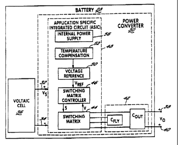
Fig. 2 is an electrical block diagram of a battery interposing a power
converter
between a voltaic cell and terminals of the battery.
Fig. 3 is an electrical block diagram of a battery including a power converter
comprised of an Application Specific Integrated Circuit (ASIC) and an output
capacitor
and a fly capacitor.
Fig. 4 is an electrical circuit for a noninverting switching matrix, fly
capacitor, and
output capacitor of Fig. 3.
Fig. 4A is an electrical circuit of an inverting switching matrix, fly
capacitor, and
output capacitor of Fig. 3.
Fig. 5 is a three-dimensional plot of stored charge in the fly capacitor as a
function
of source voltage (VS) and the capacitance of the fly capacitor (CF).
FIGS. 6A and 6B are a representative complex impedance plots as a function of
frequency for a high efficiency capacitor, specifically an 8 F ultra-capacitor
sold by
Maxwell as a model Ultra PC223.
Fig. 7 is an electrical circuit for an illustrative circuit for a first
comparator
demonstrating an approach for the switching matrix controller of Fig. 4.
Fig. 8 is a voltage plot, during the time interval required for the output
capacitor to
charge, of a switch signal to the switching matrix of Fig. 4 generated by the
first
comparator of Fig. 7 in response the plotted output voltage sensed at the
output capacitor.
Fig. 9 is the voltage plot of Fig. 8 for a longer period of time to show
steady-state
operation of the power converter.
Fig. 10 is an electrical circuit for a switching matrix controller utilizing a
comparator biased by a voltage divider for a predetermined threshold.
CA 02377166 2001-12-12
WO 01/01553 PCTNS00/17272
_g_
Fig. l0A is a representative voltage plot over time for the switching matrix
controller of Fig. 10 showing a desirable hysteresis in switch commands for
the switching
matrix as the output voltage varies around the predetermined threshold.
Fig. 11 is an electrical block diagram of a second comparator for the
switching
matrix controller of Fig. 10.
Fig. 11 A is a first pair of a differential amplifier followed by a hysteresis
decision
amplifier for the second comparator of Fig. 11.
Fig. 11B is a second pair of a differential amplifier followed by a hysteresis
decision amplifier for the second comparator of Fig. 11.
Fig. 11 C is a self biasing amplifier for the second comparator of Fig. 11.
Fig. 11D is a pair of inverters for the second comparator of Fig. 11.
Figs. 12A-12D are voltage plots representative of the second comparator shown
in
Figs. 11, 11A-11D, specifically the Fig. 12A includes the first differential
amplifier,
hysteresis decision amplifier pair, Fig. 12B includes the second differential
amplifier,
hysteresis decision amplifier pair, Fig. 12C includes a self biasing
amplifier, and Fig. 12D
contains a pair of inverters.
,Fig. 13 is the voltage plots of Fig. 12B and 12D for the initial charge-up
period of
the output capacitor.
Fig. 14 is an electrical block diagram for a third comparator for the
switching
matrix controller of Fig. 10.
Fig. 14A is a pair of differential amplifiers with built-in hysteresis for the
comparator of Fig. 14.
Fig. 14B is a Schmitt trigger for high gain rail-to-rail for the comparator of
Fig.
12.
Fig. 14C are three inverters for the comparator of Fig. 14 to square off the
switching points.
CA 02377166 2001-12-12
WO 01/01553 PCT/US00/17272
-9
Fig. 15A is the current drawn in conjunction with the switching matrix status
shown in Fig. 15B for the circuit of Figs. 14, 14A-C.
Fig. 16 is an electrical circuit for a single-stage boost chain internal power
supply
for the Application Specific Integrated Circuit (ASIC) of Fig. 3 with Fig. 16A
depicting a
clocking signal to properly sequence the circuit.
Fig. 17 is an electrical circuit for a multi-stage boost chain internal power
supply
for the Application Specific Integrated Circuit (ASIC) of Fig. 3 with Fig. 17A
depicting a
clocking signal to properly sequence the circuit.
Fig. 18 is a voltage plot over time for each stage of the multi-stage boost
chain
internal power supply of Fig. 17.
FIG. 19A is a top-level diagram of an output stage for a buck power converter.
FIG. 19B is a top-level diagram of an output stage for a boost power
converter.
FIG. 20 is one version of a circuit for a start-stop controller for the boost
power
converter of FIG. 19B.
FIG. 21 is a timing diagram for the start-stop controller of FIG. 20.
Detailed Description of the Invention
Dynamic Control of a Power Converter
Refernng to Fig. 2, an electrical block diagram of a battery 28 includes a
power
converter 30 interposed between input terminals 32, 34 of a voltaic cell 36
and a positive
output terminal 38 and negative output terminal 40 of the battery 28. The
power
converter 30 comprises a switched capacitive device 42 across a positive and
negative
output terminals 38, 40 whose mode is switched by a switching matrix 44. The
switching
matrix 44 is controlled by a signal S from a switching matrix controller 46
that generates
the signal S in response to a measurement M received from the switching matrix
44.
CA 02377166 2001-12-12
WO 01/01553 PCT/US00/17272
- 10
Fig. 3 is an electrical block diagram of a battery 28 of Fig. 2 showing
additional
aspects of the invention. For example, the power converter 30 may utilize a
switched
capacitive device 42 in the form of an output capacitor CoUT across the
terminals 38, 40
and a fly capacitor CFLY. The output capacitor CoUT arid the fly capacitor
CFLY are also
electrically coupled across respective portions of the switching matrix 44. A
portion of
the power converter 30 may include an Application Specific Integrated Circuit
(ASIC) 48
incorporating the switching matrix 44 and switching matrix controller 46. For
some
applications utilizing voltaic cells 14 having a relatively low nominal source
voltage VS,
the ASIC 48 may further include a voltage reference 50, preferably extremely
low power
consuming with good stability, providing a reference voltage (Y~F) signal to
the
switching matrix controller 46. Since some voltage references 50 may vary as a
function
of semiconductor temperature, temperature compensation 52 to the voltage
reference SO
may also be included, such as a proportional-to-absolute-temperature circuit.
Voltaic
cells 14 such as lithium electrochemical cells have an inherent bandgap
voltage reference
that may utilized. As will be shown in more detail below, the ASIC 48 may
further
include an internal power supply 56 which allows efficient operation of other
portions of
the ASIC 48 at relatively low voltage levels of the source voltage VS.
Capacitive-Only Power Converter (Charge Pump)
Fig. 4 is an electrical circuit for a noninverting switching matrix 44', fly
capacitor CgLy, and output capacitor CoUT of Fig. 3, and depicts a simplified
voltage
doubler. During the first half cycle during a charge mode, switch signal S 1
commands
switch Q1 and switch Q3 closed, switch signal S2 commands switch Q2 and switch
Q4
closed, and capacitor CFLY charges to Vs. During the second half cycle, switch
signal S 1
conunands switch Q 1 and switch Q3 open, and switch signal S2 commands switch
Q2
and switch Q4 closed, and CFLY is level shifted upward by VS volts. This
connects the fly
CA 02377166 2001-12-12
WO 01/01553 PCT/US00/17272
-11
capacitor CFLY to the output capacitor CoUT, allowing energy to be delivered
to the output
as necessary. The actual voltage is slightly lower than 2 x VS, since switches
Q1-Q4 have
resistance that drains charge from CoUT~
The power efficiency of a switched capacitive device 42 is affected by three
factors: the internal losses in the ASIC 48, the resistive losses of the
capacitors CFLY,
COUT~ and the conversion losses during charge transfer between the capacitors
CFLY, COUT~
The total power loss is:
P LOSS - P LOSS INTERNAL LOSSES + P PUMP CAPACITOR LOSSES + P CONVERSION
LOSSES
where (1) the internal losses are associated with the IC's internal functions,
such as
driving the switches, etc. (These losses are affected by operating conditions
such as input
voltage, temperature, and frequency); (2) the switch losses occur because of
the on-
resistance of the MOSFET (Metal Oxide Semiconductor Field Effect Transistor)
switches
in the IC; and (3) the charge-pump capacitor losses occur because of the
Equivalent Series
Resistance (ESR) of the fly capacitor and load capacitor.
The relationship between these losses and the output resistance is as follows:
_ 2 ~~
PPUMP CAPACITOR LOSSES + PSWITCH LOSSES - ZO X ~UT
~UT = ~l~ ~OSC X CFLY ~~ + Z RSWITCHES + 4 ESRCFLY + ESRCOUT
where fosc is the oscillator frequency. The first term ROUT is the effective
resistance from
an ideal switched-capacitor power converter 30.
As the output current io increases, the output voltage Vo of the battery 28
droops.
The voltage droop VDxooP equals the output current io drawn from the battery
28 times
the output resistance of the battery ROUT, as follows:
uDROOP - l0 X ~UT
VO=ZXVS-VDROOP
CA 02377166 2001-12-12
WO 01/01553 PCT/US00/17272
-12
Conversion losses occur during the charge transfer between the fly capacitor
CFLY
and the load capacitor CouT when there is a voltage difference between them.
The power
loss is:
PCONVERSION - ~(CFLY~2) x (4VZS-V20) + (CouT~2)x(2Vo x V~ppLE - VZ~ppLE)~
XfOSC~
where V~ppLEIS the peak-to-peak output voltage ripple determined by the output
capacitor
CouT and load current io.
To maintain the lowest output resistance ROUT, one should use capacitors CFLY
CouT with low ESR. The charge pump output resistance ROUT is a function of the
ESR
of the fly capacitor CFLY and load capacitor CoUT and the internal switch
resistance, as
shown in the equation below. Minimizing the ESR of the load capacitor CouT
minimizes
the total resistance RpUT. Using a larger flying capacitor CFLY reduces the
output
impedance and improves efficiency. Above a certain point, increasing the
capacitance of
the fly capacitor CpLy has a negligible effect because the output resistance
ROUT becomes
dominated by the resistance and capacitance of the internal switches. But when
space is a
constraint as in most batteries, it may be necessary to trade-off an
achievable lower output
resistance ROUT for the sake of small capacitor size.
A capacitance value for the fly capacitor CFLY of about 10 uF or more is
sufficient
to supply the specified load current. Surface-mount ceramic capacitors within
this
capacitance range are suitable for a number of application for the fly
capacitor CFLy, due
to their small size, low cost, and low equivalent series resistance (ESR). To
ensure proper
operation over the entire temperature range, ceramic capacitors with X7R (or
equivalent)
low-temperature-coefficient dielectrics may be used advantageously.
Increasing the output capacitance value of the output capacitor CoUT reduces
the
CA 02377166 2001-12-12
WO 01/01553 PCT/US00/17272
-13-
output ripple voltage V~ppLE. Decreasing its ESR reduces both output
resistance ROUT
and ripple V~ppLE. Increasing the capacitance of the output capacitor CoUT
reduces the
output ripple voltage. Decreasing its ESR reduces both output resistance and
ripple.
Smaller capacitance values can be used with light loads. The following
equation to
calculate the peak-to-peak ripple:
vRIPPLE - ZO ~ ~OSC X LOUT) + Z X ZO X ESRCOUT
The output capacitor CoUT stores the charge transferred from the flying
capacitor
CgLy arid services the load between charge/discharge cycles. A good general
rule is to
make the output capacitance CouT at least ten times greater than that of the
flying
capacitance.
In a start-stop mode, power converter 30 switches only as needed to keep
output
voltage at the desired value. Also for light loads and voltages above lower
threshold
output voltage, the switching matrix 44 is completely turned off. This mode is
dominant
in the case of a power converter 30 with high efficiency capacitors because
the large value
of capacitance acts as a secondary battery. In this mode, ripple V~ppLE
depends mostly
two parameters: charge transfer between the capacitance values of CFLY and
CouT, and
the ESR of CoUT.
High efficiency capacitors are those types of capacitors having relatively low
charge leakage, for example double layer electrolytic capacitors (e.g.,
capacitors known as
super capacitors, ultra capacitors, and power capacitors) and pseudo
capacitors.
The ESR ripple contribution occurs as the output capacitor CoUT charges. The
charging current creates a negative voltage pulse across the ESR of the output
capacitor
CouT that recedes as the output capacitor CouT charges. At equilibrium, when
the voltage
on the fly capacitor CFLY approaches that on the output capacitor CoUT, no
charging
CA 02377166 2001-12-12
WO 01/01553 PCT/US00/17272
-14
current flows. This effect is even more pronounced in the case of a high
efficiency
capacitor.
The ripple contribution due to charge transfer between capacitors CFLY, CouT
creates a pulse as charge flows to the output capacitor CoUT. Adding the two
terms does
not determine peak-to-peak ripple because their peaks do not occur at the same
time. It is
the best to use the dominant term. The expression for the ripple component due
to the
ESR of CouT is:
VRIPPLE(ESR) - g X L C VS ' 2 V02 J ~,/OSC J X L ESRCOUT ~ ~ R02 X CFLY O
The expression for the ripple component predominantly due to charge transfer
is:
VRIPPLE(ESR) - 2 x ~ ( VS - 2 Vp 2 ) ~, fOSC ~ x ~ 1 ~ ( ROUT x ( CFLY + LOUT
) ) ~ , where RpUT
is open-loop output impedance. If the ESR of the output capacitor CoUT is very
small, as
is likely when ceramic capacitors are used, V ~ppLE (TRANSFER)dOmlnateS. If
the ESR is
relatively large, as with low-cost tantalum capacitors, then V ~ppLE ~ESR)
dominates.
Continuous mode is a constant frequency mode when the charge pump power
converter 30 works continuously. The expression for dominant ripple is thus:
VRIPPLE - l0 ~ ~fOSC X COUT~ + 2 X to X ESR COUT
In case of a high efficiency capacitor, the output voltage is quasi-linear so
ripple is almost
an irrelevant parameter.
In an initial starting mode, switches Q1 and Q2 may be advantageously preset
to
an "on" state to provide initial charge to the output capacitor CoUT to
prevent parasitic
latch-up of the ASIC 48, especially for electro voltaic cells having a nominal
voltage of
about 1.2 V to about 1.5 V. After the switching matrix controller 46 is loaded
by an
internal power supply (not shown) and after the fly capacitor CFLY is charged,
then
normal operation is performed.
CA 02377166 2001-12-12
WO 01/01553 PCT/US00/17272
-15
Fig. 4A is an electrical circuit of an inverting switching matrix 44", fly
capacitor
CpLy, and output capacitor CouT of Fig. 4, illustrating the advantages of
dynamic
switching of a capacitive power converter 30 to achieve an inverted output. In
the latter
as shown in Fig. 4A, rather than adjusting upward the positive voltage
potential at the
positive terminal 38, the negative voltage potential at the negative terminal
40 is lowered,
by selectively switching switches SWO and SWI.
Fig. 5 is a three-dimensional plot of stored charge in the fly capacitor CFLY
as a
function of source voltage VS and the capacitance of the fly capacitor CFLY~
FIGS. 6A and 6B are a representative complex impedance plot as a function of
frequency for an ultra-capacitor, specifically an 8 F ultra-capacitor sold by
Maxwell as a
model Ultra PC223, illustrating its beneficial low impedance.
Fig. 7 is an electrical circuit for an illustrative circuit for a first
comparator 53
demonstrating an approach for the switching matrix controller 46 of Fig. 4.
The capability that such a comparator 53 provides when used to dynamically
switch the switching matrix 44 will be shown below. In short, fly capacitor
CFLY should
advantageously be switched only when needed in a closed-loop approach, and not
based
on an open-loop oscillator approach. The basic idea is to switch the fly
capacitor CFLY
into the discharge mode when the output capacitor Cps reaches a certain
predetermined
threshold voltage (V 1 ). At this point, the fly capacitor CFLY will charge
the output
capacitor CpUT. When the output capacitor Co~T reaches a certain voltage (V2),
the fly
capacitor CFLY is switched out, and back to the voltaic cell 36 to be charged.
The key
here is to only switch based on these voltages.
The comparator 53 utilizes M1/M2 as measure points for the switch. It is
important to note that this is an illustrative representation, based on only
ideal models. A
CA 02377166 2001-12-12
WO 01/01553 PCT/US00/17272
- 16
generic comparator 53 is used to demonstrate the general operations of the
dynamic
switching matrix controller 46.
Fig. 8 is a voltage plot during the time interval required for the output
capacitor
CouT to charge. For this simulation, component values were chosen as follows:
R2 = 6
kS2; R3 = 1 kS2; R4 = 6 kS2; RS = 1 kS2; R6 = 100 kS-2; R7 = R8 = R9 = 10 kS2;
R10 = R11
= 25 kS2; C3 = 10 pF; C4 = CS = 1 pF. Depicted is a voltage plot of a switch
signal S 1 to
the switching matrix 44 switches Q 1 and Q3 of Fig. 4, this signal S 1 being
generated by
the first comparator 53 of Fig. 7. Also plotted is the output voltage Vo
sensed at the
output capacitor CouT and returned to the first comparator 53 as measured
signal M2.
One aspect of the operation of the comparator 53 evident from Fig. 8 is how
the switching
rate varies depending on the load on the battery 28.
Fig. 9 is the voltage plot of Fig. 8 for a longer period of time to show
steady-state
operation of the power converter 30, reinforcing the dynamic operation of the
comparator
53 to the load demand.
Fig. 10 is an electrical circuit for a switching matrix controller 46
utilizing a
comparator 53 biased by a voltage divider 54 for a predetermined threshold.
Fig. l0A is a representative voltage plot over time for the switching matrix
controller 46 of Fig. 10 showing a desirable hysteresis in switch commands for
the
switching matrix 44 as the output voltage varies around the predetermined
threshold. For
this simulation, the component values for Fig. 10 were chosen to be as
follows: R22 = 1
MS2; R23 = 40 kS2; R24 = l OMS2; R27 = 1 MS2; R28 = 200 kS2; C21 = 22 pF.
Fig. 11 is an electrical block diagram of a second comparator 53' for the
switching matrix controller 46 of Fig. 10. Specifically, a series arrangement
is depicted of
a differential amplifier 55, differential amplifier 56, hysteresis decision
amplifier 57,
hysteresis decision amplifier 58, self biasing amplifier 59, inverter 60 and
inverter 61.
CA 02377166 2001-12-12
WO 01/01553 PCT/US00/17272
-17
Fig. 1 lA is a first pair of the differential amplifier 55 followed by a
hysteresis
decision amplifier 56 for the second comparator 48' of Fig. 11.
Fig. 11B is a second pair of the differential amplifier 57 followed by the
hysteresis
decision amplifier 58 for the second comparator 48' of Fig. 11.
Fig. 11 C is the self biasing amplifier 59 for the second comparator 48' of
Fig. 11.
Fig. 11D is a pair of the inverters 60, 61 for the second comparator 48' of
Fig.
11.
Figs. 12A-12D show voltage plots representative of the second comparator 48'
shown in Figs. 11, 1 lA-D, specifically the Fig. 12A includes the first
differential
amplifier 64, hysteresis decision amplifier 65 pair, Fig. 12B includes the
second
differential amplifier 66, hysteresis decision amplifier 67 pair, Fig. 12C
includes a self
biasing amplifier 68, and Fig. 12D contains a pair of inverters 69, 70.
Fig. 13 is the voltage plots of Fig. 12B and 12D for the initial charge-up
period of
the output capacitor CouT.
Fig. 14 is an electrical block diagram for a third comparator 48" for the
switching matrix controller 46 of Fig. 10. In particular, a series arrangement
is depicted
of a first and second differential amplifier with built-in hysteresis 72, 73,
a high gain rail-
to-rail 74, and a first, second and third inverter 75, 76, 77.
Fig. 14A is a pair of differential amplifiers with built-in hysteresis 72, 73
for the
comparator 48" of Fig. 14.
Fig. 14B is a Schmitt trigger 74a for high gain rail-to-rail for the
comparator
48" of Fig. 14.
Fig. 14C are three inverters 75, 76, 77 for the comparator 48" of Fig. 14 to
square
off the switching points.
Fig. 15A is the current drawn in conjunction with the switching matrix status
shown in Fig. 15B for the comparator 48" of Figs. 14, 14A-C.
CA 02377166 2001-12-12
WO 01/01553 PCT/US00/17272
-18-
Fig. 16 is an electrical circuit for a single-stage boost chain internal power
supply
56a for the Application Specific Integrated Circuit (ASIC) 48 of Fig. 2 with
Fig. 16A
depicting a clocking signal to properly sequence the circuit.
Fig. 17 is an electrical circuit for a multi-stage boost chain internal power
supply
56b for the Application Specific Integrated Circuit (ASIC) 48 of Fig. 2 with
Fig. 17A
depicting a clocking signal to properly sequence the circuit. The multi-stage
boost chain
internal power supply 56b is formed from a series combination of two single-
stage boost
chain internal power supply 56a', 56a".
Fig. 18 is a voltage plot over time for each stage 56a', 56a" of the mufti-
stage
boost chain internal power supply 56b of Fig. 17.
It should be appreciated by those skilled in the art having the benefit of the
instant
disclosure that, although the capacitive switching matrix 44 is shown with one
load
capacitor CouT and one fly capacitor CFLY, more than two capacitors may be
employed to
achieve a desired capacitance. Moreover, although a one-stage capacitive
charge pump
26 is shown, a plurality of stages may be employed to further adjust the
voltage potential
(Vo) at the terminals 38, 40 of the battery 28. Additionally, the battery 28
having a built-
in dynamically-switched capacitive power converter 30 may include one or more
voltaic
cells 36. Furthermore, although the power converter 30 is illustrated as being
advantageously incorporated into a battery 28, various versions consistent
with aspects of
the invention would be separate components and/or utilize other types of
energy sources
12.
In addition, although a comparator 53 is shown as providing a closed-loop
control
function that provided advantageous dynamic switching control, those skilled
in the art
will recognize that other closed loop designs that perform some form of
comparison may
be substituted, with either tightly regulated or unregulated voltage
thresholds. This
allows, for example, the elimination of an oscillator open-loop control
function.
CA 02377166 2001-12-12
WO 01/01553 PCT/US00/17272
-19
Start-stop PWM control of an inductive-capacitive power converter
Referring to FIG. 19A, a top-level diagram of a buck power output stage 80a
for a
power converter 82a is depicted, as an example of a step down power converter
that
provides an output voltage Yo that is less than the input voltage Vs. The buck
output
stage 80a is coupled to an energy source 12 at input terminals 24, 25 and to a
load device
14 at output terminals 26, 27 to deliver energy from the energy source 12 to
the load
device 14. The energy source 12 provides an input voltage Ys and an input
current is.
The load device 14 receives a current io and an output voltage Yo.
The buck output stage 80a includes a switch MS, a rectifying element MR, an
inductive element, such as an inductor L, and a capacitance element, such as a
load
capacitor CouT. The load capacitor CouT has its positive terminal 84 coupled
to the
positive output terminal 26 and its negative terminal 86 coupled the negative
output
terminal 27, which is also coupled to the negative input terminal 25 forming a
ground
reference. The load capacitor CouT, thus, is charged to the output voltage Yo.
The
inductor L has its positive end 88 coupled to a node having a feedback voltage
VF. The
feedback voltage VF is related to a voltage VL across the inductor L. The
inductor L has
its negative end 90 coupled to the positive output terminal 26.
The rectifying element MR, implemented as a MOSFET configured as a
synchronous rectifier, has its positive terminal (source) 92 coupled to the
feedback
voltage node VF and its negative terminal (drain) 94 coupled to the negative
input and
output terminals, 25, 27. The rectifying element MR closes in response to a
control signal
S 1. The MOSFET of the rectifying element MR has a channel that conducts
current in
the reverse direction, and thereby acts like a diode by having the source and
drain
reversed compared to the MOSFET switch MS. The switch MS has its positive end
(drain) 96 coupled to the positive input terminal 24 and its negative end
(source) 98
CA 02377166 2001-12-12
WO 01/01553 PCT/US00/17272
-20-
coupled to the feedback voltage node VF. The switch MS closes in response to
control
signal S2 turning ON.
During the discharge state, the control signal S 1 is ON to close the
rectifying
element MR so that it conducts and the control signal S2 is OFF to open the
switch MS,
allowing the inductor L to discharge into the load capacitor CL. During the
charge state,
the control signal S 1 is OFF to open the rectifying element or make it non-
conductive MR
and the control signal S2 is ON to close the switch MS, allowing the inductor
to be
energized by the input current is from the energy source 12.
Refernng to FIG. 19B, a boost power output stage 80b for a power converter 82b
illustrates a configuration suitable for increasing (boosting) the output
voltage ho with
respect to the input voltage Vs. The load capacitor CouT has its positive
terminal 84
coupled to the positive output terminal 26 and its negative terminal 86
coupled the
negative output terminal 27, which is also coupled to the negative input
terminal 25
forming a ground reference. The load capacitor CpUT~ thus, is charged to the
output
voltage Yo. The inductor L has its negative end 90 coupled to the node having
a feedback
voltage VF and its positive end 88 coupled to the positive input terminal 24.
The inductor
voltage VL is defined between the input terminal 24 and the feedback voltage
node VF.
This inductor voltage VL is thus equivalent to the feedback voltage hF minus
the input
voltage Ys.
Rectifying element MR has its negative end 94 coupled to node VL, the positive
terminal 84 of the load capacitor CpUT arid thus also to the positive output
terminal 26.
The rectifying element MR has its positive end 92 coupled to the feedback
voltage node
VF. MOSFET switch MS has its positive end (drain) 96 coupled to the feedback
voltage
CA 02377166 2005-O1-18
28778-126
21
node VF and its negative end (source) 98 coupled to the
negative input and output terminals 25,27.
During the discharge state, the MOSFET switch MS
opens in response to control signal S2 turning OFF and
rectifying element MR closes in response to control signal
S1 turning ON, coupling the energy source 12 and inductor L
to the load capacitor CL. Thus, the input voltage VL and
inductor voltage VL are added in order to boost the output
voltage Uo imparted to the load capacitor CL. During the
charge state, MOSFET switch MS closes in response to control
signal S2 turning ON, coupling the inductor L across the
energy source 12. Rectifying element MR opens in response
to control signal S1 turning OFF, disconnecting the load
capacitor CouT from the energy source 12 and inductor L.
In accordance with one aspect of the present
invention, the buck power output stage 80a of FIG. 19A and
the boost power output stage 80b of FIG. 19B are both
advantageously efficient and operable with a low input
voltage (e.g., sub-one volt) by implementation as an
integrated circuit fabricated in a 0.35 micron double
salicide process (two metal, two poly salicide) utilizing
MOSFET transistor switches capable of low threshold (e. g.,
sub-one volt) control. In addition to having a low
threshold control, the MOSFET devices have a low on-
resistance, directly contributing to the efficiency of the
power output stage 80a and 8b used in accordance with the
invention.
Referring to FIG. 20, a start-stop power converter
82b utilizes a start-stop controller 100 to switchably
control the power output stage 80b of FIG. 19B. Generally
CA 02377166 2001-12-12
WO 01/01553 PCT/US00/17272
-22-
known power converters, including inductive power converters, continue to
oscillate,
even when a low demand from the load device 14 makes oscillation by the power
converter inefficient. Consequently, the start-stop controller 100
advantageously stops
the oscillation of a Pulse Width Modulation (PWM) output when the load
capacitor CoUT
is adequately charged.
Specifically, the boost power output stage 80b is as described above in FIG.
19B,
except for the addition of a capacitive element C1 coupled across input
terminals 24, 25
which is used to enhance the stability of input voltage Ys.
The start-stop controller 100 is responsive to input signals for pulse width
modulation (PWM), and oscillated control of the power output stage 80b by
selectively
generating the control signal S 1 to close the rectifying element MR during
the discharge
state and to open the rectifying element MR during the charge state, and
selectively
generating the control signal S2 to open the switch MS during the discharge
state and to
close the switch MS during the charge state. The start-stop controller 100
senses a low
demand as indicated by the comparison of the reference voltage Y~F from a
voltage
reference 104 and the output voltage Yo to hysteretically stop the oscillated
control signal
so that the output stage 80b remains in the discharge state. The start-stop
controller 100
includes a hysteretic comparator 106 responsive to the reference voltage VHF,
the output
voltage Yo and the feedback voltage YF to generate a duty-cycle signal, and
hysteretically
responsive to the output voltage Yo and the reference voltage VHF to generate
a stop
signal. A modulator 108 generates an oscillation signal having the
predetermined
frequency from a fixed-frequency oscillator 110. An SR flip flop 112 is set by
the set
duty-cycle signal and reset by the oscillation signal to produce a switching
signal which
determines the charge state and the discharge state. A multiplexes 114 is
responsive to
the switching signal to generate the control signals S 1 and S2. The
multiplexes 114 has a
CA 02377166 2001-12-12
WO 01/01553 PCT/US00/17272
- 23
predetermined state switching delay to mitigate cross conduction of the power
output
stage 80b. The multiplexer 114 is also responsive to the stop signal to stop
oscillations
until more energy is needed by turning OFF control signal S2 to open switch MS
and by
turning ON control signal S 1 to close rectifying element MR.
In addition, a start-up circuit 116 biases the start-stop controller 100 when
the
power output stage 80b is discharged, as well as providing initial charge to
the load
capacitor CL.
Refernng to FIG. 21, the operation of the start stop power converter 82a is
shown
in a timing diagram. The source voltage VS tends to decay over time in many
applications, such as an energy source 14 comprised of electrochemical voltaic
cells,
eventually falling below the nominal voltage rating VNOM for that class of
energy source
12.
The output voltage Vp is initially below two voltage thresholds, VoFF and
Vorr~
The duty cycle of the switching between charge and discharge states is a
predetermined
value considering the capacitive and inductive values of the components and
the desired
output voltage Vo, with the duty cycle responding to the decline in the source
voltage VS
to maintain the output voltage Yo. The operation of switching duty cycle
continues until
a time A when the output voltage Yo is greater than the voltage threshold
VoFF,
whereupon the hysteretic comparator 70 signals the multiplexer 114 to stop
outputting the
switching signals S 1 and S2, opening the rectifying element MR and switch MS.
The
load device 14 draws stored energy from the output capacitor CpUT, drawing
down the
output voltage Vo until it drops below the voltage threshold VoFF. However,
the
comparator 70 hysteretically responds by waiting until time B, when the output
voltage
CA 02377166 2001-12-12
WO 01/01553 PCT/US00/17272
-24-
Vo drops below the voltage threshold VoN, before signaling the multiplexer 114
to
recommence switching signals S 1 and S2.
The invention in its broader aspects is therefore not limited to the specific
details,
representative apparatus and methods, and illustrative examples shown and
described.
Accordingly, departure may be made from such details without departing from
the spirit
or scope of applicants' general inventive concept.