Note: Descriptions are shown in the official language in which they were submitted.
CA 02377315 2002-03-19
TITLE OF THE INVENTION
Method for the synthesis and characterization of supported metal
nanoclusters of controlled size, surface distribution, shape and interfacial
adhesion.
FIELD OF THE INVENTION
[0001] The present invention relates to nanoclusters. More specifically, the
present invention is concerned with a method for synthesizing and
characterizing metal
nanoclusters having a controlled size, surface distribution, shape and
interfacial
adhesion.
BACKGROUND OF THE INVENTION
[0002] in the booming field of nanotechnologies, efforts are being made to
provide nanostructures usable in nanoelectronics, under the form of quantum
dots,
single electron transistors, nanophotonic devices for instance, in the
manufacturing of
chemical products such as highly specialized catalyzers, and far the purpose
of.
superconductivity as well. Such applications require mastering the sizes,
distributions
and adhesions of nanoaggregates.
[0003] A number of deposition methods have been used in constructing
nanoclusters. The e-beam method suffers from law throughput because of serial
lithographic methods. Stranski-Krastonov growth requires the initial formation
of a
strained epitaxy, with subsequent growth progressing through uncontrolled
Ostwald
ripening, leaving residual metal between clusters. Nanoclusters deposited onto
substrates, even under the most precisely controlled mass selection
conditions, are
subject to size distributions and thermodynamically determined shapes.
[0004] The precise control of nanoclusters properties, such as size, lateral
surface position and positional stability, is necessary for applications such
as supported
heterogeneous catalysts, magnetic and optical data starage media and others
where
CA 02377315 2002-03-19
2
size, lateral position and shape influence the optical, magnetic, electronic
and chemical
properties. The precise control of nanocfuster alignment and stability is
necessary in the
fabrication of nanostructures, and in the fabrication of material requiring
precise
alignment to achieve their optimum material conductivity potential.
OBJECTS OF THE INVENTION
[0005] An object of the present invention is therefore to provide an improved
method for synthesizing and characterizing metal nanoclusters having a
controlled size,
surface distribution, shape and interfacial adhesion.
BRIEF DESCRIPTION OF THE DRAWINGS
[0006] In the appended drawings:
[0007] Figure 1 is a curve illustrating the peak separation of the C1 s XPS
spectrum of the HOPG surface after a 2 keV Ar+-treatment for 10 min;
[0008) Figure 2 is a curve showing angle-resolved C1 s XPS intensities for
both the untreated HOPG surface and the same surface after a 2 keV Ar+-
treatment for 4
min;
[0009] Figure 3 shows (a) the C2:Cto~, peak intensity ratio as a function of a
duration of a 2 keV Ar+-treatment at 0° (perpendicular) and 70°
take-off angles,
respectively; (b) the result of a SRIM simulation of a 2 keV Ar+ damage at a
beam angle
of 57°.
[0010] Figure 4 is a contact AFM image of Cu clusters on a 2 keV Ar+-treated
HOPG surface, wherein the dimensions are in microns;
CA 02377315 2002-03-19
3
[0011] Figure 5 shows the C2 component relative intensity and the Cu cluster
number density on HOPG as functions of the duration of an Ar+-treatment ;
[0012] Figure 6 shows the Cu cluster coalescence kinetics on HOPG having
different surface defect densities ;
[0013] Figure 7 illustrates the effect of surface defects on the Cu cluster
coalescence coefficient ;
[0014] Figure 8 illustrates the Cu cluster size effects on the Cu cluster
coalescence kinetics for Ar+-treated HOPG surfaces having the same defect
density (2
keV Ar+ irradiation for 4 mm) ;
[0015] Figure 9 illustrates the dependence of the coalescence parameter on
the Cu cluster size for HOPG treated with 2 keV Ar+ for 4 min ;
[0016] Figure 10 illustrates the coalescence coefficient for different initial
Cu
cluster sizes, as a function of 2 keV Ar+ irradiation time ;
[0017] Figure 11 shows high resolution (a) C 1s, (b) O 1s, (c) Si 2p and (d) N
1 s XPS spectra for a Cyclotene surface treated with a 3 keV NZ+ beam for 20
min;
[0018] Figure 12 is a graph showing atomic concentrations of Cyclotene as a
function of exposure to a 3 keV N2+ beam;
[0019] Figure 13 is a graph showing changes in the component peaks of (a)
C 1 s, (b) O 1 s and (c) Si 2p XPS spectra of Cyclotene as a function of
exposure to a 3
keV N2+ beam;
CA 02377315 2002-03-19
4
[0020) Figure 14 is a graph showing relative atomic concentrations as a
function of take-off angle for Cyclotene exposed to a 3 keV N2+ beam for 20
min;
[0021) Figure 15 is a graph showing relative concentrations of (a) C 1 s, (b)
O
1 s, (c) Si 2p, and (d) N 1 s XPS spectral peak components of Cyciotene, as a
function of
take-off angle, on exposure to a 3 keV N2+ beam for 20 min; and
[0022] Figure 16 illustrates the coalescence kinetics of a nominal 8 h Cu
deposit on Cyciotene that was (a) untreated and (b) treated with a 3 keV N2+
beam for 20
min.
DESCRIPTION OF THE PREFERRED EMBODIMENT
[00231 The present description refers to a number of documents, the
content of which is herein incorporated by reference in their entirety.
[0024] Generally stated, the present invention provides a method for
controlling the deposition of copper aggregates on dielectric surfaces.
[0025] More precisely, the present invention provides a method for
controlling the sizes of copper nanoaggregates deposited on dielectric
substrate and
their distributions on the surface thereof. Additionally, the present
invention provides a
method allowing enhancing the adhesion of such copper nanoaggregates on the
surfaces they are deposited on.
[0026] Therefore, the present invention provides for repeatabilibly
controlling
the size and the distribution of copper aggregates deposited on dielectric
surfaces.
[0027] The present invention stems from the observation that copper, when
deposited by vaporization on dielectric surtaces, does not wet the dielectric
surtaces,
CA 02377315 2002-03-19
such as, for example, the Dow Cyclotene Polymer and the highly oriented
pyrolytic
graphite, known as "HOPG". On the contrary, instead of forming smooth layers
on such
surfaces, vaporized copper forms nanoaggregates. The size of these
nanoaggregates is
of the order of nanometers. The way these nanoaggregates are arranged on the
dielectric surfaces is assessed through their distribution, which relates to
the number
thereof per unit surtace.
[0028j More specifically, it is found that the copper nanoaggregates are
generally spherical in shape, with a diameter of a few manometers.
[0029j Studies on the mechanisms of the formation of such nanoaggregates,
of their adhesion properties on a substrate, and on coalescence mechanisms
yielding
larger aggregates have been undertaken.
[0030] In particular; on the one hand, chemical and physical techniques,
such as plasma treatment, ion beams method, are tested to modify the surtaces
of
substrates in order to act on the interfacial adhesion. On the other hand,
methods for
modifying the dimensions and distributions of the nanoaggregates by using ion
beams
are developed. Finally, ion beams are used to reach both targets: to control
the
nanoaggregates and to modify interfacial adhesion.
[0031] That is, it is shown herein that evaporated and sputtered metals
deposit, onto several insulating substrates important to the microelectronics
industry, in
the form of nanoclusters. While such nanoclusters tend to be spherical, those
deposited
by gentle landing from the gas phase, using cluster deposition tools (seeded
supersonic
nozzle sources, gas aggregation sources, etc.), have non-spherical
(icosahedral, etc.)
shapes. Nanoclusters that do float adhere well to substrates undergo lateral
diffusion
and coalesce in vacuum, with the coalescence kinetics being inversely related
to the
extent of cluster-substrate adhesion.
CA 02377315 2002-03-19
6
Ar+ Induced Surface Defects on HOPG and Their Effect on the Nucleation,
Coalescence
and Growth of Evaporated Copper L
[0032] In a first aspect of the present invention, it is shown that a
component
peak of the Class XPS spectrum in Ar+-irradiated HOPG, at 285.6 eV, is due to
surface
defects. This is done by demonstrating a strong correlation of the component
with the
size and number density of the Cu cluster.
[0033] Further, the coalescence behavior of Cu clusters on HOPG having
different surface defect densities caused by Ar+ ion irradiation is
investigated. It is found
that, on the one hand, the growth of larger clusters takes place through
cluster
coalescence, and, one the other hand, that, as the cluster size approaches
atomic
dimensions, the growth takes place through Ostwald-like ripening.
[0034] Finally, a model for nucleation and growth, in which deposited atoms
and small clusters interact with defect sites and are immobilized to some
extent, is
described.
[0035] Firstly, the motivation for the works yielding the method of
the.present
invention will be described.
[0036] An understanding of the nucleation, initial growth and coalescence of
metallic clusters on thin films at the initial stage of deposition is of prime
importance in
the production of nanoscale structures and devices, and it has been motivating
many
theoretical and experimental recently. Due to their importance in industrial
chemical
catalysis, metal clusters or nanoparticles on oxide substrates have been
extensively
investigated and documented over the last two decades [1-8]. In addition,
HOPG, due to
its well-defined surtace structure and weak interactions with metals, has been
widely
CA 02377315 2002-03-19
7
used in the study of supported metal clusters deposited from the vapor [9-23J
or as size-
selected clusters [24-26J.
(0037] Much progress in the understanding of the nucleation, initial growth
and coalescence of metallic clusters on thin films at the initial stage. of
deposition has
recently been made through the use of high-resolution in-situ STM [3-7, 26J.
An
interesting aspect of metal cluster diffusion on the HOPG surface is that the
value of the
diffusion coefficient, "D", is surprisingly found to be greater than expected,
sometimes
reaching 10-a cm2/s [27-28J
(0038] Although scanning transmission electron microscopy, or "STEM", was
initially used to study nucleation, growth and coalescence [29, 32), the
limitation of in-
situ, time-dependent observations led researchers to combine STEM with
molecular
dynamics simulations [7,27,28]. While STM/AFM has an obvious potential in the
study of
in-situ cluster coalescence, growth and surface diffusion behavior, these
techniques may
suffer from tip convolution effects [33-37J, even for tips giving atomic
resolution on flat
terraces. This has caused most researchers to use clusters heights instead of
cluster
diameters. In fact, there are stilt tip limited-size effects from height
measurement results
[37J if the separation between clusters is not large enough compare to the tip
dimension.
(0039] It was found eisewere by the present applicants [38, 39J, that XPS can
be used in the estimation of the average cluster diameter and has been used in-
situ to
determined time-resolved coalescence and growth without the limitations of
surface'
topography and surface conductivity. Additional interfacial chemical and
compositional
information is also provided with high sensitivity.
[0040j Although surface defects are generally considered to be one of the
most important factors for nucleation, growth and coalescence [7, 24, 25, 40-
44J, there is
still little quantitative, systematic description of their effect on these
properties. Those
surface defects created by low energy Ar+ radiation on HOPG have been
investigated by
CA 02377315 2002-03-19
8
Raman spectroscopy. This was done through monitoring the ordered Raman-active
E2g
peak at 1580 em-' (the so-called "G mode"), and that at 1356 cm's ("D mode")
due to the
onset of disorder effects [45-48j. It was previously shown that the D:G peak
intensity
ratio was influenced by disorder and related to its length (see Nakamura and
al., [47-
48j). AES was used to evaluate surface damage effects induced by low energy
rare gas
ion sputtering by analyzing the C(KLL) peak shape change due to the appearance
of a
high-energy shoulder; this method is limited by the SIN of the spectrum (See
Steffen and
al. [49,50]).
[0041] Surface probe microscopy, particularly STM with its superior space
resolution, has been extensively used to study surface damage induced by low
energy
ion bombardment [51-66j. The general results of these studies are the
following:
(1 )the surface exhibits protrusions or hillocks, separated by flat terraces
on which
normal atomic order is observed;
(2) the number of hillocks depends on the incident ion dose and energy; and
(3) the average dimensions of the hillocks are insensitive to the ion incident
energy
and species.
[0042] Generally, there are some difficulties in using STM to distinguish
surface point defects [56-57], because STM images of vacancy defects ("VD")
and
interstitial defects ("ID") have contributions from both the states and the
geometry of a
focal electron. It was suggested in the past [60, 64j that one type of defect
could be
distinguished from the other by measuring the local tunneling barrier height
(~) and
tunneling spectroscopy (trough an I-V curve). However, a question remains
concerning
how to relate the defect density with hillock density. Indeed, it is difficult
to separate the
number point defects in a STM image of a single hillock. In addition, the
observed
surface defect states may also be influenced by the surface state of the probe
tip [44j.
[0043] XPS, one of the most sensitive surface techniques, has also been
used to analyze HOPG surface structure and HOPG surface damage [67-70j. It was
CA 02377315 2002-03-19
9
previously suggested [68] that the X-ray excited Auger line referred to as
"C(KLL)" may
be used to evaluate the relative concentrations of sp2 and spa hybridization
in a-C thin
films. The increase of asymmetry on the high energy side of the C(KLL)
spectrum was
then attributed, upon Ar~ ion irradiation, to the onset of disorder. It was
further suggested
in the past [69] that the change of C1s peak asymmetry under irradiation is
due to the
production of a spa component (Jackson and Nuzzo). Such an explanation however
is in
conflict with the previous AES results [49,50].
[0044) For their part, the present applicants have previously proposed [70]
that the change in asymmetry on the high binding energy side of the C1s
spectrum of
HOPG under Ar+ bombardment is due to an homolytic bond scission and to the
creation
of a less delocalized sp2 network. A new peak located at 285.6 eV, which is
1.0 eV
higher than the main C1s peak, is associated with a free radical site
resulting from such
a bond scission and sp2 network. This conclusion was confirmed by confocal
Raman
analysis data. fn fact, it appears that these free radical sites are the
surface defects that
are to be considered. The. purpose here is therefore to discuss these surface
defects in
terms of their effect on the nucleation, growth and coalescence Cu clusters
deposited by
evaporation.
[0045] Having introduced the general background surrounding the work
yielding to a method according to a first aspect of the present invention, a
summary of
the experimental steps at the origin of this aspect will now be given.
[0046 A component peak of the C1 s XPS spectrum was used to evaluate
surface defects induced by keV Ar+ radiation on HOPG. As explained
hereinabove, it
was previously showed that a component 1.0 eV higher than the main C1s peak at
284.6
eV, whose intensity is strongly correlated with the extent of Ar+ irradiation,
is due to less
extensive sp2 electron delocalization caused by the breaking of surtace bonds.
Here, it is
shown that, for evaporated Cu deposited onto the Ar+-treated HOPG surface,
both the
number density and average size of the Cu clusters formed are correlated with
the
surface defect density. These results also indicate that the nucleation of Cu
clusters
CA 02377315 2002-03-19
takes place at these defect sites, and that the Cu cluster must further
overcome an
energy barrier to diffuse and coalesce. The coalescence process follows the
universal
equation, d = kt", where "d" is the average cluster size, and "k" and "a" are
two
coalescence parameters influenced by the interaction between a cluster and a
substrate
surface. The Cu cluster coalescence coefficient "DS" is strongly dependent on
the
surface defect density and on the initial size of the Cu cluster. This is used
to suggest
electrostatic interactions between deposited atoms and small clusters with
defect sites.
[0047] The detailed experimental set ups will now be briefly described.
[0048] The samples of the type ZYA HOPG, having dimensions 10 mm x 10
mm and 2 mm thick, were obtained from SPI fnc: they were cleaved with adhesive
tape
just prior to each experiment and immediately inserted into a spectrometer.
[0049] XPS was carried out in a VG ESCALAB 3 Mark II, using non-
monochromated Mg Ka X-rays (1253.6 eV). The base pressure in the analysis
chamber
irvas less than 10 ''° tort. Spectral peaks were separated using an in-
house, non-linear
least mean squares program. Ar+ treatment took place in the instrument
preparation
chamber at a pressure less than 10 -'° tort, using an ion energy of 2
keV and a current
density of about 10'3 ionslcm2.s. The angle between the Ar+ beam and the
surface of a
sample was about 57°. Following the Ar+ treatment, the samples were
immediately
transferred to the analysis chamber without exposure to the atmosphere.
[0050] Copper (Cu) was also evaporated, as described in the art, at a
deposition rate of about 4 Almin, by electron beam. The nominal Cu thickness
was
monitored with a quartz crystal oscillator placed near the sample.
[0051] The results obtained using the above-described experimental set up
are now described in detail.
CA 02377315 2002-03-19
11
[0052] First, the results related to the C1s XPS spectra of Ar+-induced
surface defects and disorder will be enumerated.
[0053] As was recently shown by the present applicants [70], the C1 s XPS
spectrum undergoes the following changes under Ar+ irradiation:
(1 ) the n* ~-- ~ shakeup, at about 291.2 eV, rapidly disappears;
(2) there is an increase in asymmetry on the high binding energy side of the
main
C1 s peak; and
(3) there is an increased FWHM of the C1 s peaks, suggesting that the surface
defect formation decreases the lifetime of a hole.
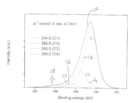
[0054] Following the Ar+ irradiation, the C1s spectrum 10 shown in Figure 1
can be separated into four components, as detailed by the present applicants
[70].
Figure 1 illustrates the peak separation of the C1 s XPS spectrum of the HOPG
surface
after a 2 keV Ar+-treatment for 10 min. Briefly, a C1 peak 12, seen at about
284.6 eV, is
attributed to extensively delocafized sp2 bonding; a C2 peak 14, at about
285.6 eV, is
attributed to more localized sp2 banding as a result of bond scission; a C3
peak 16, at
about 286.5 eV, is attributed to spa bonding; and a C4 peak 16, at about 288.0
eV, is a
shake-up of the C2 peak 14.
[0055] Figure 2 shows an angle resolution of the intensity of a C1s spectrum
for HOPG samples before (curve 20) and after (curve labeled 22) Ar+
irradiation. The
results agree with previous results in the art [67]. In particular, the
observed loss of
diffraction peaks indicates that the surface structure is destroyed to some
depth under
Ar+ irradiation. A SRFM simulation [130], at an angle of 57° gives a 2
keV Ar+ collision
event (damage) depth extending down to about 4 nm.
[0056] Similar angle resolution of the C2:C1 peak intensity ratio [70] leaves
no doubt that the C2 component occurs at or near the surface, as is confirmed
by the
CA 02377315 2002-03-19
12
time dependence of the C1 : C2 ratio at perpendicular (0°) (curve
labeled 32 in Figure
3a) and grazing (70°) (curve labeled 34 in Figure 3a) take-off angles.
It appears that the
C4 : C2 intensity ratio remains unchanged during irradiation, as does the C3
peak
intensity [70].
[0057] As determined from a SRIM simulation of 2 keV Ar+collision events as
a function of depth illustrated in Figure 3b, the averaged damage at 0°
(3 ?~ cos 8 = 4
nm) is slightly more than half the averaged damage at 70° (3 ~, cos 8 =
1.35 nm). This is
in exact agreement with the results of XPS displayed in Figure 3a.
(0058] Secondly, the results related to the initial nucleation of evaporated
Cu
on the Ar+-treated HOPG surface will now be enumerated.
[0059] A typical surface morphological AFM image of Cu clusters on the Ar+-
treated HOPG surface is illustrated in Figure 4. The clusters 40 are spherical
in shape,
as confirmed by TEM [38], and uniformly distributed on the surface 42. There
is no
preferential decoration on terrace steps, such as seen in the art for most
relatively
unreactive metal clusters on the untreated HOPG surtace [21, 24, 25; 71, 72].
[0060] Cu was evaporated on HOPG surfaces with different defect densities,
produced by different Ar+ irradiation times. The initial Cu cluster number
density was
estimated from intensity ratios in the following way:
_I" __ Ia ~~1- a d ~~°~
IS I° t-O 1-a d ~~_ (1 )
where "la~ and "IS" are XPS peak intensities from Cu cluster and substrate
respectively,
"d" is the Cu cluster average size, and "~." is the inelastic mean free path,
best referred to
as the attenuation length. "8" is the Cu coverage given by the following
relation:
O = d (2)
CA 02377315 2002-03-19
13
where "w~ is the Cu effective thickness. Therefore, substituting (2) into (1
), the following
relation is found:
Ia __ I° ~1- a d l ~°~ (3)
IS I°d-wl-eal~=
Since the Cu cluster average size d and the Cu effective thickness w are
further related
to the cluster density ~n" by the following relation:
n d 3 = w or h = w (4)
d
the following can be written:
_Ia __ Ia n d2~1-a d l~°~ (5)
IS 1° d -~ °d2~1-a d l~'S~
[0061] The cluster density n may be estimated from Equation (5) by using the
cluster average size d obtained from the cluster: substrate peak intensity
ratio. Such a
method avoids using the effective thickness and the problems related therewith
since the
effective thickness may vary with treatment.
[0062] The result is shown in Figure 5 as a function of Ar+ irradiation. It
should be noted that all the XPS data were acquired within a few minutes after
sample
deposition. The similarity of the time-dependent surface defect concentration
and the
time-dependent initial Cu cluster number density is clearly seen. This implies
that the Cu
nucleation site is located at the surface defect site.
[0063] Thirdly, the results related to the. dependence of the Cu cluster
coalescence on surface defects at room temperature will now be detailed.
[0064] Figure 6 shows the dependence of the Cu cluster coalescence on
surface defects is shown by the coalescence kinetics of Cu_ clusters on HOPG
surtaces
CA 02377315 2002-03-19
14
exposed to Ar+ treatment for different times. Although the same amount of Cu
was
deposited in all cases, the average cluster size decreases with treatment
time. Indeed;
while the coalescence is invariably given by the following the power law
described ealier
hereinabove:
d = k to (6)
where "k" and "a" are constants that depend on the defect density and on the
deposition
condition, the higher the relative surface defect concentration, the smaller
the initial Cu
cluster size.
[0065] For convenience in describing the coalescence behavior of the Cu
cluster the coalescence coefficient "DS" is used [39]. It is assumed that
surface diffusion
occurs by Brownian motion, as formalized by the following relation:
2
DS . 1 ~x ~ (7)
4 t
and that:
/x2' _ /x\2 =1/n (~)
where <x2> is the average square displacement of the cluster over time t.
Combining
Equations. (4) and (8), the following equation is obtained:
DS - 4 w3 t ('-3qt (9)
[0066] This indicates that the cluster coalescence rate depends on the
cluster size a (when a ~ 113) and on time. The time dependence of DS, for
different
surface defect densities, has been calculated from equation (9) and is
illustrated in
Figure 7. As expected, the higher the surface defect density, the lower the
value of the
coalescence coefficient. It is to be noted that the data in Figure 7 are in
reasonable
agreement with reported diffusion coefficient values determined by STM in the
art [73,
74].
CA 02377315 2002-03-19
(0067] The effect of the Cu cluster size on the coalescence is of great
concern to people in the art [27, 28, 40-44, 73]. Such effect has here been
evaluated by
the present applicants by depositing different sizes of Cu cluster on HOPG
having the
same surface defect density, through controlling the thickness of the Cu
deposition.
Figure 8 shows that there are only minor differences when the initial cluster
size is
greater than 1 nm. However, Cu clusters whose initial size is less than 1 nm
experience
a faster coalescence, as indicated by the 0.2 nm data in the Figure 8. The
dependence
of a on the cluster size is shown Figure 9, where an inverse logarithmic
relation indicates
that the larger the cluster size, the smaller the value of a.
(0068] The time dependence of DS on the cluster size .is found in Figure 10,
where all the HOPG surfaces were treated for 4 min by a 2 keV Ar+ beam, for
comparison purposes. It should be understood that a comparison of the relative
positions of the different treatments would lead to serious error, since the
time between
deposition and XPS analysis varies with the amount of Cu being deposited.
Clearly, the
value of a is essentially constant with the thickness of the deposited layer
until it
decreases to the diameter of a Cu atom.
(0069] The various results reported hereinabove were analyzed along the
following fines.
(0070] Concerning the surface defects created on HOPG by Ar+ irradiation, it
is believed that the results demonstrate that threshold energy exists for ion-
induced
defects in HOPG [49, 50]. More precisely, in the case of rare gas ions, the
threshold
energy increases linearly with ionic radius, from 22.5 eV for He to 47.5 eV
for Kr for
example. An energy of 2 keV for Ar+ was used in the above-described
experiments,
which is therefore much higher than the threshold energy for creating surface
defects.
Other possible processes for the present irradiation conditions include
sputtering, bond
scission and ion penetration. Ar+ penetration will create point defects in the
subsurface
region. As mentioned earlier, a SKIM simulation (see Figure 3b) indicates a
damage
CA 02377315 2002-03-19
16
depth of about 4nm for 2 keV Art, which is about equal to the C1 s
photoelectron probe
depth of about 4nm in HOPG. Normal collision processes lead to a non-uniform
depth
distribution for the defect density, as noted hereinabove and as confirmed by
the SRIM
simulation.
[0071] As noted by the present applicants [70], such defects are electrophilic
and; therefore, appear at higher binding energies than expected. The following
Egelfoff's
suggestion [75] is used, that states that:
~ Ea = kvI n~ (1 O)
j0072] where "n~" is a defect atom co-ordination number and "~Eb" is a
binding energy increase due to a co-ordination number reduction. The change in
the
number "Nd" of defects per unit volume induced by ion irradiation per unit
time can be
written as follows:
d Nd U - Sn Nd 11
dt r ~No - Nd~~ ( )
where "N" is the density of HOPG (known in the art as 1.25 x 10²³ atoms/cm3
[48]), "s" is
a displacement cross section, "~" is an incident ion flux, "v" is a mean
number of
displaced atoms in a cascade per primary impact (i. e., the damage function),
and "s"" is
the sputtering yield of the carbon atoms at regular HOPG sites. This gives the
following
dependence of defect density on time:
No a~t~
Nd = Cl - a ~n+6~~ ~t~ (12)
Sn -~ Sd -f- 6(~U
[0073] This result indicates that the volume defect density depends on the
ion flux ~, the damage function v, the displacement cross-section a and also
on the
sputtering coefficient s". The dashed Line in Figure 5 represents the fit to
the
experimental data.
CA 02377315 2002-03-19
17
[0074] Moreover, the saturation, which represents a maximum defect
density, is given by the following equation:
Nd (max. = No 6~U (13)
s" + 6~U
[0075] It is also possible to determine the C2 : C1 peak intensity ratio,
which
is given by the following relation:
~~u (1. a ~sR+a~u ) rJ
Nd __ Na . (14)
N No - Nd ' s" + a~v a "+~U r
[0076] Such a non-linear dependence of surface defects upon ion irradiation
was previously found in the art by using STM image analysis [22, 53]. The
hillock
number density, which represents the surface defects, so obtained was then
also
approximately proportional to the number of ion impacts (with the exception of
C+
bombardment) [53, 65] under low dose ion irradiation. This correspondence will
not hold
true when a single hillock does not correspond to a single point defect.
[0077) Turning now to the nucleation of Cu at the initial stage of deposition
on the HOPG surface, it is concluded that the cluster nucleation takes place
at surtace
defect sites. The surtace defect density induced by Ar+ ion irradiation may be
estimated
and compared with the number of clusters. As seen in Figure 5, the cluster
density for 8
A of deposited Cu varies from about 5x10"/cm2, for untreated HOPG, to about 6
x
10'31cm2 at saturation.
[0078] Two conclusions can immediately be derived from Figure 6:
(1) the maximum Cu cluster density is about 1-2 % of the surface carbon
density;
and
CA 02377315 2002-03-19
18
(2) the cluster density saturation is reached after 3 min of Ar+ irradiation,
which is
consistent with the time dependence of surface defect production.
[0079] This should be compared to Figure 3a, where, as the take-off angle is
lowered, resulting in the analysis becoming more surface-sensitive, a plot of
C2/C~°,~,, as
a function of irradiation time, shows that C2 is about 20 %, still greater
than the Cu
cluster density. This difference in cluster density and defect density
magnitudes may be
attributed to one or more of the following:
(1) a Cu cluster may sit on several defect sites; and
(2) a spectrum of cluster-defect site interaction energies may exist, with the
cluster
held only at sites where the interaction is high enough.
[0080] Indeed, metal cluster escape, also called detachment, from nucleation
sites bas been seen in the art by TEM in the case of Au clusters on AI203 [7,
43]. As
suggested by the equation (1), the defects may be single-point or mufti-point.
[0081) From the time dependence of the Cu cluster size shown in equation
(6), the time dependence of the Cu cluster number density may be determined as
follows:
n = k3 t 3" (15)
[0082] Since there is a finite time necessary between initial deposition and
XPS observation, the initial cluster number density measured must always be
less than
the nucleation density. This is another possible reasan for the difference in
cluster
density and defect density magnitudes:
[0083) In relation to the coalescence and growth of Cu clusters on HOPG, Cu
cluster coalescence on HOPG with different extents of surface defects is
illustrated in
Figure 7 and, with different amounts of initial Cu thickness on the same
surface defect
CA 02377315 2002-03-19
19
density, in Figure 8. Both cases follow equation (6), where the value of
exponent a is
often used as an indication of the growth mechanism.
[0084] In one limiting scenario, mass transport between clusters may occur
atom by atom, in which case an atom detaches from one cluster and moves to
another.
Known in the art, this process is called Ostwald ripening, with experimental
values of a
ranging from 0.25 to 0.33 [77, 78). In another limiting scenario considered in
the art,
cluster growth occurs through cluster diffusion and coalescence, with a found
to be 0.20
or less [44, 79, 80).
[0085 Despite many theoretical and experimental studies devoted to the
meaning of the value of a, there is still no generally satisfactory
understanding among
people in the art [4). Because of the importance of the value of a in
ascertaining the
cluster coalescence mechanism, a short discussion will now be presented.
(0086] The present applicants recently studied cluster growth not only
following (static) but, also, during (dynamic) Cu deposition [81]. A
comparison of a
values for the two conditions, on variously treated Cyclotene substrates, is
seen in Table
I, in which are listed values of a for static and dynamic Cu cluster growth
under various
conditions.
Surface treatmentDynamic growth Static growthAdhesion (N)
Untreated 0.32 0.14 1.8
Ar+-treated 0.34 0.12 2.6
Table I
In Table I, the specific surface treatment processes used are detailed
elsewhere [90, 91)
and the growth conditions used are explained in [81). In the case of the
static growth
(column 3), the total Cu thickness used was 8 A, deposited at 0. 1 A/s.
Finally, the
adhesion (column 4) is measured by a MicroScratch TesterT"", according to
experimental
details described in [92).
CA 02377315 2002-03-19
[0087j Cu is known to coalesce, in the static case, by the movement of whole
clusters [39], and this is reflected in the a values. However, in the dynamic
case, the a
values are substantially larger. Higher a values attributed to "Ostwald-like"
ripening were
also reported iri the art from experimental [78, 82-86] and theoretical [87-
86] studies on
both static and dynamic cluster growth. The phrase "Ostwald-like" is used here
since
there is a contribution from an atomic deposition process, as well as from an
atomic
surface diffusion. The higher a value during dynamic cluster growth may be due
to the
process domination of adatoms striking the clusters or the substrate surface
between,
and diffusing to the clusters [88]. That is, during dynamic growth, cluster
coalescence
only plays a minor rote because of its smaller a value.
[0088] As can be further seen in Table I, interfacial interaction between
cluster and substrate appears to be another factor that affects the value of
a. Stronger
interfacial interactions during static growth cause Cu retention, increasing
the density of
nucleation sites. This interaction also retards the motion of clusters across
the substrate
surface, giving slower cluster growth and a correspondingly smaller value of
a. Such a
model is consistent with the experimental data of the present applicants [38,
39, 70, 81,
90-92) and with some others reported in the art [84). Combining the static and
dynamic
results of Table I, it can be seen that, even in the case of Ostwald ripening,
cluster-
substrate interaction plays an important role.
[0089 The initial cluster size is another important factor affecting the value
of
a, as is illustrated in Figure 9. It should particularly be noted that there
is an increase of
a to 0.30 as the cluster size approaches that of an adatom, and as the cluster
migration
becomes atom migration. At the other extreme of Figure 9, clusters larger than
6 nm do
not appear to grow. A similar phenomenon was also found in the art for Pd
clusters on
Ti02 [4, 44J. Considering Figures 5 and 9, it can be seen that the surface
defect density,
through its influence on cluster size, influences a [4, 24, 25, 44j. In a
recent finding by
the present applicants, it is found that ion beams can significantly increase
the value of a
[93).
CA 02377315 2002-03-19
21
[0090] Therefore, it can be concluded conclude that the value of a is strongly
affected by the following parameters:
(1 ) the interaction between cluster and substrate surface;
(2) the initial cluster size; and
(3) the surface defect density.
[0091] From Equations {6) and {9), it is further found the following relation:
1-3a
D$ = 4 w d a (16)
indicating that the coalescence coefficient D5 decreases as the cluster size
increases, for
a less than 1/3. For static coalescence, a is less than 1/3 unless the cluster
size
approaches that of an adatom. In the case under consideration here case, a
ranges from
0.05 to 0.3, giving values of (1-3a)la in the range of 17 to 0.33.
[0092] In confirmation of Equation. 16, several experimental and theoretical
studies [73, 78, 94-102] known in the art have found a similar dependence. For
example,
it was reported that Pd clusters on Ti02 substrates show a DS ~c d'~
dependence [4, 44],
which is consistent with others' prediction [100], while it was elsewhere
suggested that
the value of a ranged from DS x d'3 to DS ~ d'' depending on the specifics of
diffusion
[94]. Still another theory indicated that DS ~c d'' [101] and a further one
predicted that DS
~ d'2 [102]. A Lennard-Jones simulation [73] indicated that the rate of
diffusion of a
cluster varies roughly as the inverse the contact area between the cluster and
the
substrate: DS ~c d-2. It was also found that Ag clusters on Ag (100) diffuse
roughly as DS
~ d''~6 indicating that the dependence of coalescence coefficient on cluster
size is
dominated by interaction between cluster and substrate [95].
[0093] The dependence of the coalescence coefficient on the initial size, as
illustrated in Figure 10, indicates that, when the size of the cluster is
atomic, the growth
CA 02377315 2002-03-19
22
occurs by Ostwald-like ripening, while, when the size is greater, the growth
takes places
by cluster coalescence.
[0094] Finally, a relationship between defect site and cluster nucleation is
presented. As previously demonstrated by the present applicants [70), Cu
deposition
onto Ar+-treated HOPG gave no evidence of chemical reaction (i. e., no carbide
was
formed) nor were there any other changes manifested in the XPS and Raman
spectra
that could be used to indicate any other sort of interaction. Thus, since some
sort of
interaction undeniably takes place, it must be very weak. Further, it must
take place
between an electropositive Cu atom and a positively charged defect site. Here
it is
suggested that this is an induced dipole-charge interaction. In such a case,
the
interaction energy "U" is
U =_ -a ez~2 r4 (16)
where a is the polarizability of a Cu atom, "e" is the charge of a site and
"r" is the site-
dipole distance. Such an interaction is very weak and short-range.
0095 Interestingly, it was recently found in the art [103), in relation on the
calculation of the properties of linear, planar and 3-dimensional Cu clusters
by density
functional theory, that all clusters a few atoms in size and greater, no
matter what their
shape, experience charge separation, meaning that atoms having the greatest co-
ordination numbers have the greatest negative charge. Thus, as the cluster
begins to
grow, it changes from an induced dipole to a permanent dipole (quadruple,
etc.) and its
adhesion to the site actually increases slightly for a short time. This may be
the reason
behind the present finding that, in some cases, larger clusters move more
easily than
atoms.
The Surface Modification of Dow Cyclotene by Low Energ~N~+ Beams and its
Effect on
the Adhesion of Evaporated Cu Films
CA 02377315 2002-03-19
23
(0096] In a secand aspect of the present invention, attention is drawn to the
surface modification of Dow Cyclotene by low energy NZ+ beams and its effect
on the
adhesion of evaporated Cu films.
0097 Basically stated, low energy (3-6 keV) N2+ beams are used to modify
Dow Cyclotene for the purpose of grafting N-containing groups onto the
Cyclotene
surface. In-situ XPS analysis demonstrates an extensive loss of aromaticity
due to bond
breaking by the beam, white angle resolution shows that implantation occurred
substantially below the Cyclotene surface. The paucity of N-containing groups
at the
outer surtace and the resultant poor adhesion of the Cu clusters permit
extensive cluster
coalescence.
[0098] As an introduction to the matter of the second aspect of the present
invention, it is reminded that Dow Cyclotene 3022, also known as "BCB", a low
permittivity insulator, is one of several candidates for near-future "ULSI"
(for Ultra Large
Scale Integration) and "GS1" (for Giga-Scale Integration) technologies,
especially in
combination with copper metallurgy. However, when Cu is deposited, either by
evaporation or sputtering, as a base layer for subsequent electrochemical
deposition, its
adhesion is generally found to be weak. There are several methods that can be
used to
promote adhesion in this case, among which the chemical modification of the
Cyclotene
surface through the use of plasmas, ion beams and lasers, in order to graft
functional
groups onto the surface. Here it is found that N2 plasma modification achieves
the
highest adhesion of evaporated Cu on the Cyclotene surface. This low energy
(below 15
eV) technique modifies the surface layer but does not penetrate below.
However, such
thin modified layers may not be mechanically adequate for device mechanical
stability.
In order to increase the modified layer thickness, low energy (in the range of
keV) ion
beam modification may be a better choice due to its implantation effects. Such
beams
have already been used in the art for polymer metallization and the surface
modification
of metals. The present aspect of the invention deals with the comparison of
law energy
N2+ beams with the previously used N2 plasma technique as a method of
modifying the
CA 02377315 2002-03-19
24
Dow Cyclotene surface. Cu cluster coalescence dynamics are used to evaluate
adhesion to the modified surface.
[0099] The experimentally steps at the foundation of the method of the
present aspect of the invention are described as follows.
[00100] Cyclotene 3022 samples were prepared as is well known to people in
the art [91,105-107, 121J. Briefly, cleaned Si wafers were treated with 1%
(w/w) aqueous
y-aminopropyl triethoxysilane followed by a 46% (w/w) solution of B-staged
Cyclotene
3022 in mesitylene. After spin deposition, the wafers were linearly heated at
a rate of
1 °C/min to 250°C, under an N2 atmosphere, and were permitted to
cool down to room
temperature, still under an N2 atmosphere, before removal. Cyclotene layers
were about
1 micron thick.
[00101] X-ray photoelectron spectroscopy was carried out as known in the art
[91, 105-107J: a VG ESCALAB 3 Mk II, operating at a pressure below 2 x 10'x'
torr, used
non-monochromated Mg Ka radiation at 1253.6 eV. High-resolution spectra were
obtained at a perpendicular take-off angle, using pass energy of 20 eV and
0.05 eV
steps. After Shirley background removal, the peaks were separated using an in-
house
non-linear least squares program, using peak shapes and widths previously
available in
the art for this material [91, 105-107, 121J. It is to be noted that, with the
exception of
angle-resolved data, the take-off angle was always perpendicular to the
Cyclotene
surface.
[00102] N2+ beam treatment of the Cyclotene took place in the instrument
preparation chamber at a pressure inferior to 10'9 torr, using a VG AG21 cold
cathode
gun, with 3-6 keV kinetic energy beams and under a working pressure of 4x 10'5
torr.
The angle between the beam and the surface was about 57°.
CA 02377315 2002-03-19
~~i~se~~E~t ~~ ~v~~c~r~ti~r~ ~4 ~~r~~c~rs~~d ~s ~r~~i~~si~ d~sc~ib~a~ ire
the art ~~, ~~~-1~~~, a~ ~ ~~t~ ~~ ~.~~.,~s. ~ h~ s~ trey ~d s~r~~b~s ~r~r~~
i~r~~di~i:~i~
tr~~~s~~rr~d t~ the: ~r~~iysis ~~~~r~~s~r ~~~i~h~~"~ ~~ir~g ~tr~~s~h~ri~ e~r~
~s~re.
~irsv, the r~s~its ~i~t~ir~~d i~~ refuting t.~ s~d°f~c~
r~~~diti~~~~i~r°
~y~~i~t~r~~ dy ~3~- ~~~r~s r~aii r~~~~~ L~ ds~ri~d.
~~'i~~~ ~ r~~ti~~~t~i~ div~~r~r~~~s ~~~r~ ~~u~c~ ~~r P~2f ~~~r~s i~~ th~3 3-~
~~~~
r~r~~. ~~~r this r~~s~r~, the ~~ii~v~rirr~ ciis~s~ssi~~ ~~ili ~~ ~~r~xi~~~d v~
the ~~r~~~ts ~~" ~ '=~e'~J
~~~~s.
~~~'~~~~ ~si~a the ~~~J, ~~~~~~~~r~t r~s~its ;~r~~i~a~ss~ d~t~rr~i~~d ~~ ih~
~r~s~~t ~~~fi~~r~ts ~~ . , ~ ~~-r ~)7~, ~h~ i~r~s~r~t ~~ s, ~~ s, ~i~i~ ~3~d ~
s s~~gutr~ a~~~r~
s~~~ratad ir~t~ t~'~ir ~~~~~~~:~lt ~~~i~s. ~h~s~ ~~~ sh~~r~ ~ ~ ;=~r< ire
~,i~i~r~ ~ '. i~i~~r~ ~ ~
sh~~.~s high r~s$~i~ri~~ ~Gj ::~~ s, ~~;~ ~ ~ s, ~~~i~~ ~r~d ~dy i~3'i s ~~~
~~~~c;tr~ ~~~~ ~
~jl~~~~~re~ ~3a'~~~C~ ~~'~~t~d'e~Jfi:~"3 c'$ ~ 'K~'~!° .''~2' ~y'F-
'~rs'i ~~~r ~~ ~Y"i~, ii~Jil~r~lr'~ ~h~ ~;~'~-°~~~i-
<3~"~s°~r~~:~d
~,~r~g~r~~r~ts ~~~~~r e~rith des'c~:~~d lira's. ~ h~ ~t~ri~~tior~s ~rf th~s~
p~~iss ~r~ gi~~r~ ire ~~l~l~
ii, which ~~~c~~r~~s the pr~s~or~t i~zø ~a~~s~ tre~t~~~f r~skaits pith th~s~
~r~ ~r~- ~~~~rr~ ~r~d
i'~a gl~s~~ tr~~tr~e~t ~s ~~t~ir~~d i~ the ~~t.
CA 02377315 2002-03-19
~ abf~ ff
[Oaf~1~ hero are some differences, =~rhich ~fviff bo discussed hur~inbef~~;w.
s hose peak fits ropresent i:he gr cat~st statistical significance
obtair~abfe, and rn~ore
c ,nsistont ever fho soon angfos ~tsvd to ob:_ain the angle-resof~rod data eve
~rifl shortf~°
disc~sss.
~~~19~~ ~-ligh-resoi~aticr ~ °i s, C3 1 s, ~i ~p and ~ 1 s ?~~~
spoctra, E~o~°
Cycfotene oxpos~;d to a ~ ko'~~ d~2~. boam vor ~~ mrn, are sfnovvn ire f=ig.
fa. ~har~ges fo~~~d
in tg a ~ is spo~;~e°ui~ ir~cl~do tf~o rapid riisappearanco ~~ tf~e r~'
a re shako-up, arid ar
as~mrr~ot~,3 on ti'~o high bir~;~ing s~s:er~~ silo cv ti~o pock as r~ev~~
co~,ponors~s aro
introduced. ~ new pock vvas ~-~fso ir~~rod~ced in ~otf~ th~r ~ 1s spocvr~r~ in
i=igurr ~'ib
and the ~i ~p sp~;ctr ~ar~ in t~~~ ~i~s~ro 1 ~ c, vy~~ile sorr~o peaks
proa~ioL~sf~ foE Bnd ~~ other
troatrrsonts X91, 1 ~~~~ pro~ic~d fir tried b~~ the ~resor~t appf icar~~s wore
absent. oho P~ r s
spectrum, shogun in Fig~sre 11d, indicates that tvvo ~-containing peaf~,s
v~~oro present,
.which suggests that. t~.ro groups may ha~ro been iratrflduced, as
pre~rio~asfy found en ~~2
pfasr~~a treatment X91]. ,~itorr»iti~efy, it mad indicate that two ~-
containing fragments
vverP implanted, as v~iif be ft~~°ti~er discussed f~oreinbofovv.
CA 02377315 2002-03-19
27
[00109] Figure 12 illustrates the evolution of the surface composition on beam
exposure time as determined by using XPS peak areas and sensitive factors. It
can be
seen that he near-surface relative N concentration increased with beam
exposure time,
while those for Si, O and C decreased.
[00110] Component evolution as a function of beam exposure time is
illustrated in Figures 13. As seen in Figure 13a, the C1 component decreases
as the C2
component increases, while the C3 and C4 components remain effectively
constant.
Thus, it can be understood that bonds are broken and electron delocalization
becomes
more localized during exposure to the beam. The -Si-O-Si- bond breaking
appears to
stabilize after 3 mm, as seen in the O 1s and Si 2p peak evolutions
illustrated in Figures
13b and 13e. While the N1 s component peak evolutions (not shown) continue to
increase with beam exposure time, the N1 : N2 ratio remains constant at 2 : 1.
[00111] The elemental depth distribution induced by a 20 min beam exposure
has been determined by angle-resolved XPS, and the results are shown in Figure
14. It
appears that both Si and O concentrations are enriched at the outer surface
while N and
C concentrations are depleted. Such changes are similar to those found for C,
Si and O
on Ar+ beam exposure [107) and indicate that, in the present experiment also,
the
surface is being sputtered by the beam. The N profile shown in Figure 14
indicates that
little N has remained at the surface. Whether this is also due to sputtering
or to
implantation will be considered hereinbelow.
[00112] Angle-resolved XPS permitted the determination of the peak
component profiles. An example is seen in Figures 15 far Cyclotene exposed to
a 3 keV
beam for 20 min. Both Figures 15a and 15d indicate that the relative
concentrations of
the C and N components are maintained as a function of depth. However, Figures
15b
and 15c indicate a disagreement, since 01 and Si1, which were previously
attributed to
the same structure (-Si-O-Si-), move in opposite directions. This will be
further discussed
hereinbelow.
CA 02377315 2002-03-19
28
[00113] Turning now to results related to Cu deposition on the modified
Cyclotene surface, it appears that no obvious changes occurred for C 1 s, O 1
s, Si 2p
and N 1 s on the evaporation of about 3ML Cu onto the treated Cyclotene
surface. The
deposited Cu formed clusters, as in previous studies made by the present
applicants
[91, 105, 106]. The initial cluster coalescence and growth was followed by
XPS. The
coalescence and growth dynamics of Cu clusters were found to be strongly
correlated
with the interaction between Cu and the Cyclotene surface.
[00114] Typical Cu cluster coalescence processes, for a nominal 8 A thick Cu,
on both untreated Cyclotene and Cyctotene pre-treated for 20 min with 3 keV
N2+, are
illustrated in Figure 16. As noted in previous studies by the present
applicants [81, 122]
on copper coalescence, cluster coalescence is made possible when interaction
between
Cu cluster and substrate surface is weak. The clusters are then able to
diffuse, and on
contact, coalesce and grow in size. It is reminded that the change in the
average size d
of Cu cluster with time t follows the power-law (6).
[00115] The present applicants previously showed that the adhesion of Cu
film, as measured by the critical load "L~" is directly related to the
coalescence
parameters k and a through the coalescence. coefficient, Dg [81, 122, 123].
The critical
load is the lowest load, measured during a microscratch test as detailed in
the art [92,
123], at which a film delamination in initially observed. The Cu film critical
load may be
estimated, in the present case, from the k and a values. !t is found to be
around 6 N.
Although this is slightly higher than that for Cu on untreated and Ar+-treated
Cyclotene
surfaces [92], it is much lower than the 1..~ value of about 17 N obtained for
Cu on the N2
plasma-treated Cyclotene surface.
[00116] The above reported results are analyzed and yield the following
points.
CA 02377315 2002-03-19
29
[00117) First, the Peak Components are considered. As was found in previous
XPS studies on treated Cyclotene and HOPG surfaces by the present applicants
[81, 91,
106-107, 122], peak attributions are difficult and, often, mufti component, as
can be
comprehended from Table II. For example, in the presence of N, the C2
component is a
combination of the free radical produced on bond breaking and the formation of
C-
NHCHO, etc. [91j. In this particular case, the free radical contribution to
this peak may
be estimated by assuming it to be the same as that formed on Ar+ treatment.
Then,
subtraction of this component gives a 10% contribution from C-NHCHO, etc. This
is
consistent with what is found for N in Figure 12.
[00118) The peak separation of the N 1s spectrum presented hereinabove
gave peaks in positions identical to those found on N2 plasma treatment. For
those N
fragments that have reacted, it is believed that the attributions are correct
here, as well.
However, some of the fragments may not have reacted and may exist
interstitially. The
fact that only two N 1s peaks exist implies that any unreacted fragments also
contribute
to those same two peaks. This is consistent with data obtained on HOPG treated
with
N2+ beams [124, 125j.
[00119) The different peak ratios, namely N1 : N2 = 1 : 1 for N2 plasma
treatment and 2 : 1 in the present case, indicate that the energy difference
(N2+ is the
major component in our N2 plasma generator [111]) plays a role in the
reaction. The role
played by the beam energy is also revealed in the free radical data in the O 1
s and Si 2p
component spectra. For example, the absence of the 01 s peak at 532.8 eV
suggests
[107J that the -Si-O free radical does not exist although the Si 2p peak at
103.0 eV
suggests that it does. One reason for this confusion is that N has a lower
electronegativity than O' and, when replacing it, as in -Si-N- and -C-N-
bonds, causes
electron density changes at photo-emitting atoms that are reflected in binding
energy
shifts. It is shown in the art for example that a trigonal N has a Pauling
electronegativity
of 3.91 while a digonal O has a Pauling electronegativity of 6.21 [126j. Using
efectronegativity arguments, group electronegativity values of 3.27 for O-CH3
and O-
C2H5, and 2.66 for NH-CH3 and NH-C2H5 are also calculated in the art [126).
Such ratio
CA 02377315 2002-03-19
is in reasonable agreement with the ratio of measured inductive substituent
parameters
elsewhere tabulated in the art [127). Thus, the apparent absence of some
component
peaks, when compared to the present N2 plasma study and the different
component
ratios may signal different reaction products due to energy differences in the
treatment
processes.
(00120] Concerning nitrogen profile and Cu adhesion, as stated hereinabove,
it is known a threshold exists for ion-induced defects in HOPG [112-114). It
is reminded
that for rare gas ions, this threshold increases linearly with ionic radius
from 22.5 eV for
He to 47.5 eV for Kr for example. There is little doubt that the threshold is
in this range
for N2+ on Cyclotene. That is, below , this threshold, N2+ is expected to
react at the
substrate surface since there would be no reason for N2+ to remain at the
surface if it has
not reacted. Above this threshold, it is expected to undergo a Coulomb
explosion,
producing N+, which penetrates into the subsurface. Moreover, some of the
fragments
may react and some may form interstitials.
(00121] A short digression on Coulomb explosions is now in order. This
phenomenon is also known as collision-induced dissociation in the art (128).
It occurs
when a projectile, such as a molecule, a molecular ion or a cluster for
example, strikes
an object, such as a gas molecule or a surface for example, with a force
sufficient to
strip one or more of its electrons. This highly charged projectile, which is
excited to a
vibrational continuum, then undergoes dissociation. In the case of 4-10 keV
N2+ ions for
instance interact with a He target to lose an electron. The N22+ tnus formed
dissociates
into 2N+.
(00122] fn the case of the present plasma system, ion energies lie below 15
eV [112,129), and little or no subsurface penetration is expected. However,
for N2+
beams in the 3-6 keV range, substantial penetration of the fragments of the
Coulomb
explosion is expected, and whether any N will remain at the surface to react
is
questionable.
CA 02377315 2002-03-19
31
[00123] In order to answer such a question, ion penetration simulations were
performed using "SRJM" (for Stopping and Range of Ions in Matter, described in
the art
[130J). Since N2+ separates into N+ that penetrates, the simulation used N+ at
1.5 keV,
resulting in each of the fragments retaining half the energy of the NZ+ ion,
with none lost
to the substrate. This is believed to be a reasonable approximation for a
massive
substrate in the art [128, 131], These ions then simulated penetrating
polymeric
substrates of densities similar to that of Cyclotene (about 0.95 g/cm3).
[00124] It is found that the penetration maximum (at around 5-6 nn) was
invariably beyond the XPS probe depth, which is about 4 nm for N. However, up
to 4 nm
in depth, the simulation profile was surprisingly similar to the profile
generated from
Figure 14. Such a simulation profile (not shown) indicates little, if any, N
at the sample
surface. Since the atomic displacement threshold is only slightly higher in
energy than
the threshold for ion-induced defects [112-114], most of the penetrating N+
may have
reacted. For those penetrating N+ that have not reacted and that therefore lie
interstitially, the possibility exists for orbital overlap with the Cyclotene
structure. For
example, N'', whose configuration is [He] 2s2 2PX 2py, may have interacted
with one side
of a 1 Egg aromatic HOMO of a benzenoid ring, in a fashion similar to what was
found for
the reaction of Cu with untreated Cyclotene by the present applicants [105].
This would
serve to reduce the formal charge on the N, reducing its binding energy.
Indeed, this
may be the reason for the higher than expected N1 : N2 ratio.
[00125] Considering that only the N2 component, at about 1l3 of the total N
concentration (see Figure 15d) represents N-containing groups capable of
interaction
with Cu [91 J, and that only those few at the surface can react, it can be
anticipated a little
increase in Cu adhesion occurs, as compared to the untreated surface. This is
indeed
found in the present case, by measuring the critical load of Cu evaporated
onto
Cyclotene, both treated and untreated [92J. Both untreated and Ar+ ion-treated
Cyclotene
have L~ values of about 2 N, while N2 plasma-treated Cyclotene has an L~
values of
about 17 N. In the present case, the estimated L~ values is about 6 N, as
determined
CA 02377315 2002-03-19
32
from a relationship between Cu coalescence and L~ demonstrated by the present
applicants.
[00126] For the purpose of a direct comparison with samples treated by N2
plasma, which were exposed to atmosphere on transfer from the plasma chamber
to the
XPS, these samples were also intentionally exposed to atmosphere for 1 min.
Such
exposure did not change the coalescence coefficient within experimental error.
That is,
the adhesion remains the same. This indicates that interfacial interactions,
rather than
beam-induced surface roughness effects, dominate the adhesion of Cu film on
Cyclotene. This is identical to what was previously found for the Ar+ ion
treatment of
Cyclotene [107].
[00127] Summarizing this second aspect of the present invention, it can be
said that XPS analysis of Cyclotene treated with 3-6 keV N2+, when compared
with N2
plasma treatment, shows that the reaction path followed depends on the energy
of the
treatment. The higher energy beam treatment resulted in penetration of the N-
containing
species into the subsurface, with few N-containing groups remaining at the
outer
surface. This results in a lower adhesion of Cu when compared to the plasma
treatment,
where N-containing groups are limited to the outer surface.
[00128] From the foregoing, it will be apparent to people in the art that the
present invention provides a method to deposit strongly adhering metallic
nanoclusters,
less than 10 nm in size, whose diameter, lateral surface positioning and
positional
stability (adhesion) are closely controlled, onto substrates of potential
interest to
industry, in the construction of nanostructures.
[00129] It will be further apparent that the present invention provides a
method
to characterize the sizes, the surface distributions, the shapes and the
stability of such
nanoclusters through the use of appropriately modified angle-resolved XPS,
supported
by Monte-Carlo simulations.
CA 02377315 2002-03-19
33
[00130] It will be also apparent that the present invention provides a method
to
vary the size and distribution of nanoclusters on substrate surfaces, such as
HOPG and
low permittivity polymers, through ion beam irradiation, and also by laser
irradiation.
[00131] It will be also apparent that the present invention provides a method
enabling the use of laser, ion beam and plasma surface treatments to
chemically modify
the substrate surface so as to react with the nanoclusters, binding them
strongly.
[00132] It will be also apparent that the present invention provides a method
enabling to determine the size, the distribution, the shape and the positional
stability of
such nanoclusters. Such a determination of some of these properties is often
difficult by
TEM, when the cluster size is at the spatial resolution limit of the
instrument. Similarly,
AFM/STM tip effects make such determinations difficult.
[00133] The present invention provides for a method to determine,
nondestructively and simply, nanocluster dimensions and surface densities by
using
XPS intensity ratios at a fixed electron emission angle.
[00134] The present invention also provides for a method to follow
coalescence kinetics, a measure of the stability of nanoclusters as well as to
identify
substrate defect sites at which cluster nucleation and growths occurs, and to
quantify
their relationship.
[00135] The present invention also provides for a method for using angle-
resolved XPS, which is an accepted technique for the non-destructive, in situ
characterization of the thickness of uniform films deposited onto surfaces, to
obtain XPS
data on clusters that, as expected, do not fit the standard model of a uniform
film with an
abrupt interface at the substrate, because, when applied to (discontinuous)
nanoclusters, the use of angle-resolved XPS requires modification. This was
achieved
CA 02377315 2002-03-19
34
by introducing modifications of the model that permit the determination of the
sizes of
nanoclusters, as well as their shapes and spatial configurations on the
substrate surfiace.
[00136] The present invention also provides for a method adapting Monte-
Carlo simulations to the study of nanoaggregates, based on the realization
that
preliminary Monte-Carlo simulations of the angle-resolved XPS data, which take
into
account nanocluster size, shape, and both size and number density
distributions,
qualitatively account for the experimental results. Therefore, the present
invention
provided for a method allowing such calculations, by demonstrating the
necessity of
including such variables in the' calculations. It is clear from these results
that a Monte-
Carlo simulation section should be included with the experimental section,
each
furnishing feedback for the other.
[00137] As will be appreciated by people in the art, the present invention
permits the construction of nanostructures and devices to be used in
nanoelectronics,
such as single electron transistors and high-density data storage for example.
[00138] Furthermore, people in the art will foresee that the present method
may allow to precisely control metal nanocluster size (less than 10 nm) and
lateral
surface positioning on substrates, through the use of laser, ion beam and
plasma
treatments. It may also allow to fix them, at specified locations, by
increasing their
adhesion through the chemical modification of selected areas on the substrate
surface,
using laser machining.
[00139) Moreover, obviously the present invention paves the way to modified
and adapted the angle-resolved XPS technique, by allowing development of Monte-
Carlo simulations of the behavior of nanoclusters on substrates; as functions
of size,
shape, surface distribution and stability. This in turn has the potential to
permit such
simulations to be used for the characterization of nanoclusters determined by
angle-
resolved XPS intensities, as well as feedback for our experimental procedures.
CA 02377315 2002-03-19
[00140] Finally, people in the art will appreciate that the method of the
present
invention, while enabling to control nanoaggregates in a simple way, in a
cluster tool for
example, without exposure to the atmosphere, can be easily extended to
semiconducting substrates, permitting the growth of nanoclusters while
avoiding the
restrictions imposed by Stranski-Krastonov growth.
(00141] As people skilled in the art may also consider, the precise control of
nanocluster alignment and stability achieved by the method of the present
invention may
be used for fabricating superconductive devices, of various shape and form, to
conduct
power.
(00142] Although the present invention has been described hereinabove by
way of preferred embodiments thereof, it can be modified, without departing
from the
spirit and nature of the subject invention as defined in the appended claims.
CA 02377315 2002-03-19
36
REFERENCES
1. C.T. Campbefl, Surf. Sci. Rept. 27(1997) 1.
2. C.E. Pofrer, B.K. Hance, J.M. White, J. Phys. Chem. 97 (1993} 5965.
3. C.R. Henry, Surf. Sci. Rept. 31 (1998)231.
4. M.J.J. Jak, C. Konstapel, A. van Kreuningen, J. Verhoeven, J.W.M. Frenken,
Surf. Sci. 457 (2000) 295.
5. 5. Gan, Y. Liang, D.R. Baer, A.W. Grant; Surf. Sci. 475 (2001 ) 159.
6. C.E.J. MitcheII,A. Howard, M. Camey, R.G. Egdell, Surf. Sci. 490 (2001 )
196.
7. J. Carrey, J.-L. Maurie, F. Petroif, A. Vaures, Phys. Rev. Lett. 86 (2001 )
4600.
8. J.E. Reddic, J. Zhou, D.A. Chen, Surf Scf. Lett. 494 (2001 ) L767.
9. A.R. Arthur, A.Y. Cho, Surf. Sci. 36 (1973} 641.
10. J.L. Sacedon, C.S. Martin, Thin Sohid Films 10 (1972) 99.
11. J.S. Maa, T.E. Hutchinson, J. Vac. Sci. Technol. 14(1977) 116.
12. I. Jirka, Surf. Sci. 232 (1990) 307.
13. W.F. Egefhoff, Jr., G.G Tibbetts, Phys. Rev. B 19 (1979) 5028.
14. V. Vijayakrishnan, C.N.R. Rao, Surf. Sci. 255 (1991 ) L516.
15. A. Humbert, M. Dayez, S: Granjeaud, P. Ricci, C.R. Henry, J. Vac. Sci.
Technol. B 9 (1991 ) 804.
16. P. Marcus, C. Hinnen, Surf Scf. 392 (1997) 134.
17. Y. Kawashima, G. Katagiri, Phys: Rev. B 59 {1999) 62.
18. G.K. Wertheim, S.B. Di Cenzo, Phys. Rev. B 37 (1988) 84.
19. Q. Ma, R.A. Rosenberg, Appl. Surf Sci. 140 {1999) 83.
20. H. Brune, Surt Sci. Rept. 31 (1998)121.
21. C.M. Whelan, C.J. Bames,Apph. Surf Sci. 119 (1997) 288.
CA 02377315 2002-03-19
37
22. H.-A. Durand, K. Sekine, K. Etoh, K. Ito, I. Kataoka, Thin Sohid Films 336
(1998) 42.
23. C. Binns, S.H. Baker, C. Demangeat, J.C. Pariebas, Surf. Sci. Rept. 34
(1999)
105.
24. C. Brechignac, Ph. Cahuzac, F. Carhier, M. de Frutos, A. Masson, C. Mory,
C. Colhiex, B. Yoon; Phys. Rev. B 57 (1998) 82084.
25. B. Yoon, V.M. Akuhin, Ph. Cahuzac, F. Carlier, M. de Frutos, A. Masson, C.
Mory, C. Colliex, C. Brechignac, Surf. Sci. 443 (1999) 76.
26. C. Binns, Surf. Sci. Rept. 44 (2001 ) 1.
27. L. Bardotti, P. Jensen, A. Hoareau, M. Treilleux, B. Cabaud, Phys. Rev.
Lett.
74 (1995) 4694.
28. P. Jensen, Rev. Mod. Phys. 71 (1999)1695.
29. C. Chapon,C.R.Henry, Surf. Sci. 106 (1981) 152.
30. M. Fliiehi, P.A. Buffat, J.-P. Bore!, Surf. Sci. 202 (1988) 343.
31. L. Bardotti, P. Jensen,A. Hoareau, M. Treilleux, B. Cabaud, Phys. Rev.
Lett.
74(1995)4694.
32. W.D. Luedtke, U. Landman, Phys. Rev. Lett. 82 (1999) 3835.
33. E.C.W. Leung, P. Markiewicz, M.C. Goh, J. Vac. Sci. Technol. B 15 (1997)
181.
34. L. Lai, E.A. Irene, J. Vac. Sci. Technol. B 17 (1999) 33.
35. S. Kitching, P.M. Williams, C.J. Roberts, M.C. Davies, S.J.B. Tendler, J.
Vac.
Sci. Technol. B 17 (1999) 273.
36. V.J. Garcia, L. Martinez, J.M. Briceno-Valero, C.H. Schilling, Probe
Microsc. 1
(1997) 107.
37. D.-Q. Yang, Y.-Q. Xiong, Y. Guo, D.-A. Da, W.-G. Lu, J. Mater. Sci. 36
(2001 )
263.
38. D.-Q. Yang, M. Meunier, E. Sacher, Appl. Surf Sci. 173(2001 ) 134.
39. D.-Q. Yang, E. Sacher, J. Appl. Phys. 90 (2001 ) 4657.
CA 02377315 2002-03-19
38
40. C.H. Herry, C. Chapton, B. Mutaftschiev, Thin Solid Films 33 (1976) Li.
41. A.D. Gates, J.L. Robins, Thin Solid Films 149 (1987) 113.
42. K.R..Heim, S.T. Coyfe, G.G. Hembree, J.A. Venabies, M.R. Scheinfein, J.
Appl. Phys. 80 (1996) 1161.
43. U. Diebohd, J.-M. Pan, T.E. Madey, Surf. Sci. 33 1-333 (1995) 845.
44. M.JaJ. Jak, C. Konstapel, A. van Kreuningen, J. Verhoeven, J.W.M. Frenken,
Surf Sci. 474 (2001 ) 28.
45. G.F. Feng, R. Zallen, J.M. Epp, J.G.. Dillard, Phys. Rev. B 43 (1991 )
8678.
46. K.K. Tiong, P.M. Amirtharaj, F.H. Pollak, D.E. Aspnes, Appl. Phys. Lett.
44
(1984) 122.
47. K. Nakamura, M. Kitajima, Appl. Phys. Lett. 59 (1991 ) 1550.
48. K. Nakamura, M. Kitajima, Surf. Sci.; 283 (1993) 255.
49. H.J. Steffen, C.D. Roux, D. Marton, J.W. Rabalais, Phys.Rev. B44 (1991 )
3981.
50. H.J. Steffen, D. Marton, J.W. Rabalais, Phys. Rev. Lett. 68 (1992) 1726;
Nucl.
Instrum. Methods Phys. Res. B 67 (1992) 308; D. Marton, K.J. Boyd, T. Lytle,
J.W. Rabalais, Phys. Rev. B 48 (1993) 6757.
51. L. Porte, M. Phaner, C.H. de Vihleneuve, N. Mobncoffre, J. Tousett, Nuci.
Instr. Methods Phys. Res.B44 (1989) 116.
52. L. Porte, C.H. de Villeneuve, M. Phaner, J. Vac. Sci. Technol. B 9 (1991)
1064.
53. R. Coratger, A. Claverie, F. Ajustron, J. Beauviilain, Surf Sci. 227
{1990) 74;
R. Coratger, A. Claverie, A. Chahboun, V. Landry, F. Ajustron, J.Beauvillain,
Surf Sci., 262 (1992) 208.
54. F. Thibaudafl, J. Cousty, E. Balanzat, S. Bouffard, Phys. Rev. Lett.
67(1991 )1582.
55. K.P. Reimann; W. Boise, U. Geyer, K.P. Leib, Europhys. Lett. 67 (1995)
463.
56. T. Li, B.V. King, R.J. MacDonald, G.R. Cotterill, D.J. OConnor, Q. Yang,
Surf.
Sci. 312 (1994) 399; Q. Yang, T. Li, B.V. King, R:J. MacDonald, Phys. Rev.
B53 (1996) 3032.
CA 02377315 2002-03-19
39
57. J.8. Hahn, H. Kang, S. Song, LC. Jeon, Phys. Rev. B 53 (1996) 81725; J.R.
Habn, H. Kang, Surf Sci. 357-358 (1996) 165.
58. M. Kappel, M. Steidi, J.Biener, J.Kuppers, Surf Sci., 387 (1997) L1062.
59. K. Mochiji, S. Yamamoto, H. Shimizu, S. Ohtani, T. Seguchi, N. Kobayashi,
J.
Appl. Phys. 82 (1997) 6037.
60. H. Ogiso, W. Mizutani, S. Nakano, H. Tokumoto, K. Yamanaka, Appl. Phys. A
66 (1998) S 1155.
61. B. An, S. Fukuyama, K. Yokogawa, M. Yoshimura, Jpn. J. Appl. Phys. 39
(2000) 3732.
62. S. 1-labenicht, Phys. Rev. B 63 (2001) 125419.
63: F. Forst, D. Hirsch,A. Schindler,Appl. Surf Sci. 179(2001)8.
64. J.8. Hahn, H. Kang, Phys. Rev. B 60 (1999) 6007.
65. K. Shimada, T. Ishimaru, T. Yamawaki, M. Uchigasaki, K. Tomiki, T.
Matsukawa, 1. Ohdomari, J. Vac. Sci. Technol. B 19 (2001 ) 1989.
66. F. Forst,A. Schindier, F. Bigl, Phys. Rev. Lett. 85(2000)4116.
67. A. Hoffman, G.L. Nyberg, J. Liesegang, Phys. Rev. B 45 (1992) 5679.
68. J.C. Laskovich, S. Scaglione,Appl. Surf Sci. 78(1994)17.
69. S.L. Jackson, R.G. Nuzzo, Appl. Surf Sci. 90 (1995) 195.
70. D.-Q. Yang, E. Sacher, Surf Sci., in press.
71. G M Francis, L Kuipers, J.R.R.A. Cleaver, R E Palmer, J. App!. Phys. 79
(1996) 2924.
72. A. Humbert, M. Dayez, S. Granjeaud, P. Ricci, C. Chapon, C.R. Henry, J.
Vac. Sci. Technol. B 9(1991 ) 804.
73. P. Deltour, J.-L. Barrat, P. Jensen, Phys. Rev. Lett. 78 (1997) 4597; L.J.
Lewis, P. Jensen, N. Combe, J.-L. Barrat, Phys. Rev. B 61(2000)16084; J.-M.
Wen, S.-L. Chang, J. W. Burnett, J. W. Evans, P. A. Thiel, Phys. Rev. Lett. 73
( 1994) 2591.
74. E. Ganz, K. Sattler, J. Clarke, Suit Sci. 219 (1989) 33.
75. W.F. Egelhoff, Jr., Surf. Sci. Rept. 6 (186) 253.
CA 02377315 2002-03-19
76. T. Meguro, A. Hida, M. Suzuki, Y. Koguchi, H. Takai, K. Yamamoto, K.
Maeda, Y. Aoyagi, J. Vac. Sci. Technol. B 19 (2001 ) 2745.
77. M. von Smoiuchowski, Phys. Z. 17 (1916) 585.
78. G. Rosenfeid, K. Morgenstern, M. Esser, G. Comsa, Appf. Phys. A 69 (1999)
489.
79. D. Kandel, Phys. Rev. Lett. 79 (1997) 4238.
80. J. Eggers, Phys. Rev. Lett. 80 (1998) 2634.
81. D.-Q. Yang, E. Sacher, in Metallization of Pplymer 2, E. Sacher, ed.,
Kluwer,
New York, in press.
82. M. Gautier-Soyer, S. Gota, L. Douillard, J.P. Duraud, P. Le Fevre, Phys.
Rev.
B 54 (1996) 10366.
83. S. Xu, B.L. Evans, D.I. Flynn, Cao En, Thin Solid Films 238 (1994) 54.
84. R.L.W. Smithson, D.J. McCiure, D.F. Evans, Thin Sohid Films 307 (1997)
110.
85. C. Winkler, A. Carew, R. Rayai, J. Ledieu, R. McGarth, Surf Rev. Lett. 8
(2001 ) 693.
86. L. Zhang, F. Cosandey, R. Persaud, T.E. Madey, Surt Sci. 439 (1999) 73.
87. J.A. Blackman, A. Wihding, Europhys. Lett. 16(1991)115.
88. J.A. Venables, Surf Sci. 299f300 (1994) 798.
89. H. Schmeisser, Thin Sohid Films 22 (1974) 83.
90. D.-Q. Yang, E. Sacher,Appl. Surf Sci. 173 (2001 ) 30.
91. D.-Q. Yang, L. Martinu, E. Sacher, A. Sadough-Vanini, Appl. Surf. Sci. 177
(2001 ) 85.
92. A. Sadough-Vanini, D.-Q. Yang, L. Martinu, E. Sacher, J. Adhesion 77 (2001
)
309.
93. D.-Q Yang, E. Sacher, in preparation.
94. C. De W. van Siclen, Phys. Rev. Lett. 75 (1995) 1574.
CA 02377315 2002-03-19
41
95. J:W. Wen, S.-L. Chang, J.W. Burnett, J.W. Evans, P.A. Thiel, Phys. Rev.
Lett.
73 (1994)2591.
96. H.C. Kang, P.A. Thief, J.W. Evans, J. Chem. Phys. 93 (1990) 9018.
97. A.F. Voter, Phys. Rev. B 34 (1986) 6819.
98. A.F. Voter, SPIE Proc. 821 (1987) 214.
99. M. Zinke-Aifmang, L.C Feldman, M.H. Grabow, Surt. Sci. Rept. 16 (1992)
377.
100. E.E. Grude, J. Appl. Phys. 38(1967)243.
101. P. Meakin, in Phase Transitions and Critical Phenomena, Eds. C. Domb and
J.L. Lebowits, Academic Press, New York, 1988, p. 335.
102. E. Ruckenstein, B. Pulvermacher, J. Catai. 29(1973)224.
103. P.B. Balbuena, P.A. Derosa, J.M, Seminario, J. Phys. Chem. B 103 {1999)
2830.
104. J. Carrey, J.-L. Maurice, F. Petroif, A.Vaures, Surf Sci., in press
105. D.-Q. Yang, S. Poulin, E. Sacher, C. Hyett, Appl. Surf Sci., 165 (2000)
116.
106. D-Q. Yang, E. Sacher, E.M. Griswold, G. Smith, Appl. Surf. Sci., 180
(2001 }
200.
107. D.-Q. Yang, E. Sacher, Appl. Surt. Sci., 173 (2001 ) 30.
108. K.W. Paik, H.S. Cole, R.J. Saia, J.J. Chera, J. Adh. Sci. Technol., 5
(1993)
403.
109. N. Schiihler, P. Oeihafen, J. Vac. Sci. Technol., AIS (1997) 2529.
110. F.S. Shieu, M.H. Shiao, J. Adh. Sci. Technol., 12(1998)19.
111. A. Hallil, O. Zabeida, M.R. Wertheimer, L. Martinu, J. Vac. Sci.
Technol., A18
(2000) 882.
112. M. Collaud, S. Nowak, O.M. Kuttel, P. Groning, L. Schlapbach, Appl. Surf.
Sci., 72 (1993)
113. H.J. Steffen, D. Marton, J.W. Rabelais, Nucl. Instrum. Methods, B67
{1992)
308.
114. D. Marton, K.J. Boyd, T. Lytle, J.W. Rabelais, Phys. Rev., B48 (1993)
6757.
CA 02377315 2002-03-19
42
115. L. Zhang, K. Takata, T. Yasui, H. Tahara, T. Yoshikawa, Mater. Chem.
Phys.,
54 (1998) 98.
116. J-S Cho, W-K Choi, S-K Koh, K-H Yoon, J. Vac. Sci. Technol., B16 (1998)
1110.
117. G. Mesyats, Y. Klyachkin, N. Gavrilov, A. Kondyurin, Vacuum, 52(1999)285.
118. A. Caballero, D. Leinen, J.P. Espinos, A. Eernandez, A.R. Gonzalez-Elipe,
Surt. Interface Anaf., 21 (1994) 418.
119. M. Guemmaz, A. Mosser, J.-J. Grob, R. Stuck, Surf. Coat. Technol., 100-
IOl
(1997) 353.
120. D.L. Williamson, J.A. Davis, P.J. Wilbur, Surf. Coat. Technol., 103-104
(1998)
178.
121: S. Poulin, D.-Q. Yang, E. Sacker, C. Hyett, T.H. Ellis, Appi. Surf. Sci.,
165
(2000) 15.
122. D.-Q. Yang, E. Sacker, J. Appl. Phys., 90 (2001 ) 4768.
123. D.-Q. Yang, E. Sacker, in Proceedings of the 25t" Annual Meeting of the
Adhesion Society, Adhesion Society, Blacksburg, VA, 2002, in press.
124. J.A. Taylor, G.M. Lancaster, J.W. Rabelais, J. Amer. Chem. Soc., 100
(1978)
4441.
125. Z.W. Deng, R. Souda, Surf. Sci., 288 (2001 ) 393.
126. D. Bergmann, J. Hinze, in Electronegativity, edited by K.D. Sen, C.K.
Jrargensen, SpringerVerlag, New York, 1987, p. 145.
127. C. Hansch, A. Leo, R.W. Taft, Chem. Rev., 91(1991)165.
128. J. Los, T.R. Govers, in Collision Spectroscopy, edited by R. G. Cooks,
Plenum, New York,1978, Chapter 6.
129. 0. Zabeida, L. Martinu, J. Appi. Phys., 85 (1999) 6366.
130. http://www.srim.ora.
131. D.S. Gemmeil, Chem. Rev., 80(1980)301.