Note: Descriptions are shown in the official language in which they were submitted.
CA 02377454 2002-03-19 ' '
- Fleming-Peterson-Thomson 19-1?-43
BROADBAND ANTENNA STRUCTURE
FIELD OF THE INVENTION
The present invention relates to antennas.
BACKGROUND OF THE INVENTION
A balun is an electromagnetic device for interfacing a balanced
impedance, such as an antenna, with an unbalanced impedance. A
balanced impedance may be characterized by a pair of conductors, in the
presence of a ground, which support the propagation of balanced signals
therethrough. A balanced signal comprises a pair of symmetrical signals,
which are equal in magnitude and opposite in phase. In contrast, an
unbalanced impedance may be characterized by a first conductor for
supporting the propagation of unbalanced (i.e., asymmetrical) signals
therethrough with respect to a second conductor (i.e., ground). A balun.
converts the balanced signals propagating through the balanced
impedance to unbalanced signals for propagating through the unbalanced
impedance, and vice versa.
Baluns have been employed in various applications. One such
application for baluns is in radio frequency ("RF") antenna structures.
An antenna structure typically comprises at least one balanced impedance
- for radiating and/or capturing electromagnetic energy - coupled with a
receiver, transmitter or transceiver by means of an unbalanced
impedance. For example, an antenna structure formed from a balanced
transmission line may be coupled with the
receiver/transmitter/transceiver through an unbalanced transmission line
CA 02377454 2002-03-19 ' '
Fleming-Peterson-Thomson 19-17-43
formed from a SO S2 coaxial cable. Here, a balun is employed as an
interface between the balanced transmission line and the 50 S2 coaxial
cable.
The inclusion of a balun, however, has a limiting effect on the
frequency response of an antenna structure. Antenna structures using
baluns typically radiate and/or capture electromagnetic energy within a
singular frequency band. By incorporating a balun, multiple antenna
structures are required to support a number of frequency bands. For
example, a mufti-purpose wireless device might require a first antenna .
structure to support a cellular phone (900 MHz) band, a second antenna
structure to support a personal communication services (2 GHz) band,
and a third antenna structure to support an air-loop communication
services band (4 GHz).
The frequency limitations of baluns in antenna structures has now
become a problem. Presently, a growing commercial interest exists in
providing an increasing number of applications and services to multi-
purpose wireless devices. In an effort to minimize the additional antenna
structures required for each of these increased services; and thereby
reduce the complexity of the overall mufti-purpose wireless device,
industry has begun to explore a singular antenna structure . having a
broader frequency response characteristics. Consequently, an alternative
to the balun is needed to increase the number of frequency bands
supported by a singular antenna structure.
SUMMARY OF THE INVENTION
CA 02377454 2004-07-09
3
We have invented an antenna structure capable of supporting an
increased number of frequency bands. More particularly, we have invented an
interface between the balanced impedance and an unbalanced impedance,
which does not have the balun's limiting effect on an antenna structure's
frequency response. In accordance with the present invention, a slotline
couples an antenna structure formed from a balanced transmission line, for
example, with an unbalanced transmission line, such as a coaxial cable, for
example. We have recognized that the frequency response of an antenna
structure may be broadened by replacing a balun with a slotted transmission
line (e.g., slotline).
In accordance with one aspect of the present invention there is provided
an antenna structure comprising: at least one planar antenna element having a
balanced impedance, an unbalanced impedance, and a transmission network for
coupling the at least one element with the unbalanced impedance, characterized
in that the transmission network has a balanced impedance and includes at
least
one balanced impedance slotline for coupling the at least one planar antenna
element with the unbalanced impedance, and the at least one slotline supports
the propagation of a TEm" mode.
BRIEF DESCRIPTION OF THE DRAWINGS
The present invention will be better understood from reading the
following description of non-limiting embodiments, with reference to the
attached drawings, wherein below:
FIG. 1 is a perspective view of a known antenna structure;
FIG. 2 is a perspective view of an embodiment of the present invention;
CA 02377454 2004-07-09
3a
FIG. 3 is a perspective view of another instantiation of the present
invention;
FIG. 4(a) is a perspective view of a known slotted transmission line,
while FIG. 4(b) illustrates the electric and magnetic fields of the known
slotted
transmission line of FIG. 4(a);
FIG. 5 is a perspective view of a known element; and
FIG. 6 is a process flow of an aspect of the present invention.
CA 02377454 2002-03-19 ' '
Flerning-Peterson-Thomson 19-17-43
DETAILED DESCRIPTION OF THE PRESENT INVENTION
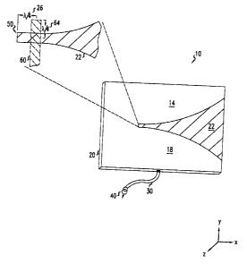
Referring to FIG. 1, a perspective view of a known antenna
structure 10 employing a balun is shown. Antenna structure 10 radiates
and/or captures electromagnetic energy. Antenna structure 10 has a
balanced configuration. More. particularly, antenna structure 10
comprises a first and a second conductive filin or leaf, 14 and 18, formed
on a dielectric substrate 20. First and second conductive leaves, 14 and
18, support the propagation of balanced signals therethrough - i.e., a
symmetrical pair of signals which are equal in magnitude and opposite in
phase. Separating first and second leaves, 14 and 18, is an expanding
non-conductive, tapered slot 22. Tapered slot 22 exposes the dielectric
characteristics of substrate 20 such that antenna structure 10, as depicted,
has a planar, travelling wave design. As shown, antenna structure 10
may be classified as an endfire-type because it radiates andlor captures
electromagnetic energy from its exposed end - i.e., in the direction of the
x- axis.
Coupled with antenna structure 10 is an unbalanced impedance 30.
Unbalanced impedance 30 comprises a first conductor for supporting the
propagation of unbalanced (i.e., asymmetrical) signals therethrough with
respect to a second conductor (i.e., ground). Unbalanced impedance 30
commonly comprises a coaxial cable - particularly with respect to
wireless and radio frequency devices. Unbalanced impedance 30,
however, may be realized by various unbalanced substitutes and
alternatives. As shown, unbalanced impedance 30 is coupled with a
radio frequency device 40, such as a receiver, transmitter or transceiver.
CA 02377454 2002-03-19
Fleming-Peterson-Thomson 19-17-43
Antenna structure 10 couples first and second conductive leaves,
14 and 18, with unbalanced impedance 30 by means of a balun 50.
Balun, 50 converts a balanced signal propagating through first and second
conductive leaves, 14 and 18, to an unbalanced signal for unbalanced
impedance 30, and vice versa. In this manner, the operation of balun 50
may be modeled as a transformer having one side of its secondary coils
grounded.
Balun 50 comprises a pair of tuned transmission line ends or stubs
to perform this conversion function. More particularly, on the exposed .
1D dielectric side of substrate 20; balun 50 comprises a stub 26 formed from
tapered slot 22. Balun 50 further comprises a second stub 64 formed
from a conductive strip or stripline 60. Stripline 60 and second stub 64
are formed on the underside of substrate 20 - opposite to the side of
conductive leaves, 14 and 18. Consequently, balun 50 comprises stubs,
26 and 64, separated by a dielectric in the form of substrate 20, for
coupling conductive leaves, 14 and 18, with unbalanced impedance 30.
The length of each stub, 26 and 64, of balun 50 is measured to provide
constructive interference from the electromagnetic wave reflections
propagating through conductive leaves, 14 and 18, and conductive
stripline 60. For example, the length of each stub, 26 and 64, is
approximately one-quarter wavelength (~,/4) from the desired frequency.
The inclusion of balun 50, however, has a limiting effect on the
frequency response of antenna structure 10. While each stub, 26 and 64,
supports the electromagnetic coupling necessary for balun 50 to convert
balanced signals to unbalanced signals, and vice versa, both stubs after
CA 02377454 2002-03-19 ' '
Fleming-Peterson-Thomson 19-17-43
the frequency response of antenna structure 10. Consequently, by
incorporating an increasing number of baluns - and thereby a greater
number of stubs - the frequency response of antenna structure 10 may be
characterized as having an increasingly narrower passband transfer
function.
The passband transfer function of an antenna structure employing a
balun has now become a problem. Presently, a growing commercial
interest exists in providing an increasing number of services to wireless
devices. In an effort to minimize the additional antenna structures
required for each of these increased services, and thereby reduce the
complexity of such a wireless device, industry has begun to explore a
singular antenna structure having a broader frequency response. As
such, an alternative to balun 50 is needed to widen the frequency
response and increase the number of frequency bands supported by a
singular antenna structure.
Referring to FIG. 2, a perspective view of an embodiment of the
present invention is illustrated. Here, an antenna structure 100 is shown
employing an alternative to a balun. Antenna structure 100 has a broader
frequency response and supports an increased number of frequency bands
than antenna structure 10 of FIG. 1.
As shown, antenna structure 100 comprises a first and a second
balanced impedance, 110 and 130, each of which realize an antenna
element. It will be apparent to skilled artisans that antenna structure 100
may comprise any number of antenna elements (i.e., one or more) in
accordance with the present invention. First antenna element 110 of
CA 02377454 2002-03-19 ' '
Fleming-Peterson-Thomson 19-17-43
antenna structure 100 comprises a first and a second conductive film or
leaf, 105 and 115, supporting the propagation of balanced signals
therethrough. Similarly, second antenna element 130 comprises a third
and a fourth conductive leaf, 125 and 135; supporting the propagation of
balanced signals therethrough. First and second leaves, 105 and 115, of
first antenna element 110, as well as third and a fourth conductive leaves,
125 and 135, of second antenna element 130 are separated from each
other by a pair of non-conductive, expanding tapered slots 140a and
140b. Tapered slots 140a and 140b expose the dielectric characteristics
of a dielectric substrate 120.
Antenna structure 100 has a planar, travelling wave design. Both
first and second antenna elements, 110 and 130, are coupled in parallel
with one another such that antenna structure 100 may be classified as an
endfire type, radiating or capturing electromagnetic energy along the x-
axis. To ensure the propagation of electromagnetic energy along the x-
axis, however, antenna elements, 110 and 130, are driven - radiating
andlor capturing - in phase with one another. Moreover, by the
expanding shape of tapered slots 140a and 140b, each antenna element,
110 and 130, may have a Vivaldi configuration. Vivaldi or tapered slot
antenna elements are known to have wider frequency response
characteristics than other antenna element configurations, such as dipole
antennas. For more information on Vivaldi and tapered slot antennas,
see, for example, K. Fong Lee and W. Chen, "Advances in Microstrip
and Printed Antennas," John Wiley & Sons (1997). It will be apparent
to skilled artisans upon reviewing the instant disclosure, however, that
CA 02377454 2002-03-19 ' '
Fleming-Peterson-Thomson 19-17-43
antenna structure 100 may have alternative configurations, designs and
classifications, while still embodying the principles of the present
invention.
Coupled with antenna structure 100 is an unbalanced impedance .,
150. Unbalanced impedance 150 comprises a first conductor in which
unbalanced signals propagate therethrough with respect to a second
conductor (i.e., ground). Unbalanced impedance 150 may be realized by
a coaxial cable, though various substitutes and alternatives will be
apparent to skilled artisans upon reviewing the instant disclosure.
Unbalanced impedance 150 is coupled with a radio frequency device 160,
such as a receiver, transmitter or transceiver. Unbalanced impedance
150 comprises an outer conductor 152a (i.e., the ground) which is
electrically and mechanically coupled (e.g., soldered) with first antenna
element 110, and a center conductor 152b (i.e., the first conductor)
which is electrically and mechanically coupled (e.g., soldered) with
second antenna element 130. The coupling of a coaxial cable with a
balanced impedance is shown in greater detail in FIG. 5.
Antenna structure 100 couples first and second antenna element,
110 and 130, with unbalanced impedance 150 by means of a slotted
transmission network. In accordance with the present invention, this
slotted transmission network converts a balanced signals propagating
through each set of conductive leaves, 105 and 115, and 125 and 135, to
an unbalanced signal for unbalanced impedance 150, and vice versa.
However, unlike balun 50 of FIG. 1, we have observed that the slotted
transmission network of the present invention does not generally narrow
CA 02377454 2002-03-19 ' '
R
Fleming-Peterson-Thomson 19-17-43
the frequency response of antenna structure 100. Consequently, this
slotted transmission network supports an increased number of frequency
bands than is presently available in the known art:
As shown in FIG. 2, the slotted transmission network comprises a
number of slotted transmission lines. The number and configuration of
slotted transmission lines necessary to perform the conversion to replace
known balun designs is dependent on several variables. These variables
include, for example, the number of antenna elements in antenna
structure 100, as well as whether the antenna elements are coupled in .
parallel or in series. It should be noted that the dimensions and the
dielectric constant of the substrate materials correspond with the resultant
impedance of each slotted transmission line in the slotted transmission
network. The mathematical relationship between a slotted transmission
line and its resultant impedance is known to skilled artisans. For more
information on the principles involving the resultant impedance of a
slotted transmission line, see K. C. Gupta, R. Gard, I. Bahl, and P.
Bhartia "Microstrip Lines and Slotlines," Artech House (1996).
In the illustrative embodiment, first antenna element 110 comprises
a first slotted transmission line or slotline 170 extending from tapered slot
140a. Similarly, second antenna element 130 comprises a second slotted
transmission line or slotline 180 extending from tapered slot 140b. First
and second slotlines, 170 and 180, are both balanced impedances.
Slotlines, 170 and 180, each match the impedance of the antenna element
to which it is coupled. A third slotted transmission line or slotline 175 is
incorporated within the slotted transmission network for coupling first
CA 02377454 2002-03-19 '
Fleming-Peterson-Thomson 19-17-43 to
slotline 170 with second slotline 180. The slotted transmission network
of FIG. 2 further comprises a fourth slotted transmission line or slotline
190 for interfacing third slotline 175 with unbalanced impedance 150.
In an instantiation of the illustrative embodiment, each antenna
S element, 110 and 130, of antenna structure 100 has an impedance of 100
S2. As shown, antenna elements 110 and 130 are coupled in parallel with
one another by means of third slotline 175, thereby yielding a matching
impedance of 50 5~. The impedance of third slotline 175 consequently
matches that of unbalanced impedance 150 - if impedance 150 is a .
coaxial cable having an impedance of 50 S2. However, if the impedance
of unbalanced impedance 150 does not match the impedance of third
slotline 175, fourth slotline 190 may be tapered to alter the impedance
seen by unbalanced impedance 150. The degree of tapering of fourth
slotline 190 corresponds with the impedance desired - a wider mouth
taper increases the impedance viewed by unbalanced impedance 150,
while a narrower mouth taper decreases the impedance viewed by
unbalanced impedance 150. The tapering of fourth slotline 190 operates
much like the number of coils employed on a transformer for matching a
first impedance with a second impedance. The tapering of a slotted
transmission line to vary its impedance is known to skilled artisans. For
more information on the principles of tapering slotted transmission lines,
see "D. King, "Measurements At Centimeter Wavelength," Van
Nostrand Co. (1952). Consequently, we have recognized that the slotted
transmission network may be designed to effectively interface antenna
CA 02377454 2002-03-19 ' '
Fleming-Peterson-Thomson 19-17-43 I1
structure 100 with a very wide range of impedance values attributed to
unbalanced impedance.
Referring to FIG. 3, a perspective view of another instantiation of
the present invention is illustrated. Here, an antenna structure 200 is
shown employing a slotted transmission network as an alternative to a
balun. Antenna structure 200 may have a broader frequency response
and support an increased number of frequency bands than antenna
structure 10 of FIG. 1.
In contrast with antenna structure 100 of FIG. 2, antenna structure .
200 is a planar, wave design having a broadside-type configuration.
Antenna structure 200 is broadside-type because the ends of each antenna
element are closed - i.e., they do not reach the outer periphery of a
dielectric substrate 220. As such, antenna structure 200 radiates or
captures electromagnetic energy along the z- axis.
As shown, antenna structure 200 comprises four (4) balanced
impedances, 215, 225, 235 and 245, each realizing an antenna element.
Antenna elements, 215, 225, 235 and 245, are coupled in parallel with
one another by the slotted transmission network. Each antenna element
is defined by an expanding pair of non-conductive, tapered closed slots -
240a through 240d. Tapered closed slots 240a through 240d expose the
dielectric characteristics of dielectric substrate 220. Each expanding
tapered closed slot may have a horn-type shape to increase the frequency
response of antenna structure 200. Horn-type antenna elements typically
have a wider frequency response than that of a conventional slot dipole-
type antenna element. Each expanding tapered closed slot, 240a through
CA 02377454 2002-03-19 ' '
Fleming-Peterson-Thomson 19-17-4.3 12
240d, may also achieve resonance at the center of the desired frequency
range. It will be apparent to skilled artisans upon reviewing the instant
disclosure, however, that antenna structure 200 may have alternative
configurations, designs and classifications, while still embodying the
principles of the present invention.
Coupled with antenna structure 200 is an unbalanced impedance
250. Unbalanced impedance 250 comprises a first conductor in which
unbalanced signals propagate therethrough with respect to a second
conductor (i.e:, ground). Unbalanced impedance 250 may be realized by
a coaxial cable, though various substitutes and alternatives will be
apparent to skilled artisans upon reviewing the instant disclosure.
Unbalanced impedance 250 is coupled with a radio frequency device 260,
such as a receiver, transmitter or transceiver. Unbalanced impedance
250 comprises an outer conductor 252a (i.e., the ground) which is
electrically and mechanically coupled (e.g., soldered) with antenna
element 215, and a center conductor 252b (i.e., the first conductor)
which is electrically and mechanically coupled (e.g., soldered) with
antenna element 235. The coupling of a coaxial cable with a balanced
impedance is shown in greater detail in FIG. 5.
The antenna elements of antenna structure 200 are coupled with
unbalanced impedance 250 by means of the slotted transmission network,
in accordance with the present invention. This slotted transmission
network converts the balanced signals propagating through each antenna
element to unbalanced signals for unbalanced impedance 250, and vice
versa. The slotted transmission network comprises a first slotted
CA 02377454 2002-03-19 ' '
Fleming-Peterson-Thomson 19-17-43 13
transmission line or slotline 270 for coupling the first antenna element,
resulting from tapered closed slot 240x, in parallel with the second
antenna element, resulting from tapered closed slot 240b. Likewise, a
second slotted transmission line or slotline 280 couples the third antenna
element, resulting from tapered closed slot 240c, in parallel with the
fourth antenna element, resulting from tapered closed slot 240d. The
first and second antenna elements, as combined, are coupled in parallel
with the combined third and fourth antenna elements by means of a third .
slotted transmission line or slotline 275. A fourth slotted transmission
line or slotline 290 interfaces unbalanced impedance 250 with the
resultant balanced impedance created by the parallel combination of each
of the antenna elements of antenna structure 200.
In an instantiation of the illustrative embodiment, each antenna
element of antenna structure 200 has an impedance of 300 S2. As
antenna elements 215 and 225 are coupled in parallel, first slotline 270 is
designed to have a matching impedance therewith - i.e., 150 S2.
Similarly, as antenna elements 235 and 245 are coupled in parallel,
second slotline 280 is designed to have a matching impedance therewith -
i.e., 150 SZ. Third slotline 275 also couples the other two antenna
elements, yielding a total matching impedance of 75 S2. Consequently,
the impedance of slotline 290 may be designed to match that of
unbalanced impedance 250 - for example, if impedance 250 is a 75 SZ
coaxial cable. However, if the impedance of unbalanced impedance 250
does not match the impedance of third slotline 275, fourth slotline 290
may be tapered to alter the impedance seen by unbalanced impedance
CA 02377454 2002-03-19 ' '
Fleming-Peterson-Thomson 19-17-43 14
250. The degree of the taper corresponds with the amount the impedance
to be altered - a wider mouth increases the impedance viewed by
unbalanced impedance 250, while a narrower mouth decreases the
impedance viewed by unbalanced impedance 250. Consequently, if
unbalanced impedance 250 was realized by a 50 S2 coaxial cable, fourth
slotline 290 may be tapered to step down the impedance of antenna
structure 200 and create a matching 50 S2 impedance for unbalanced
impedance 250.
Referring to FIG. 4(a), a perspective view of a known slotted .
transmission line or slotline 300 is illustrated. Slotline 300 comprises a
slot on one side of a dielectric substrate 310 separating a first and a
second conductive film or leaf, 315 and 320. More particularly, slotline
300 is defined by parameters W and b, as well as the dielectric constant
of substrate 310. For more information on the mathematical relationship
between a slotted transmission line and the resultant impedance, see K.
C. Gupta, R. Gard, I. Bahl, and P. Bhartia "Microstrip Lines and
Slotlines," Artech House (1996).
Referring to FIG. 4(b), the electromagnetic field distribution of
slotline 300 is illustrated. Analyzing slotline 300 in the context of
substrate 310, the dominant mode of propagation causes the electric field
to form across the slot, and the magnetic field to encircle the electric
field, though not being entirely in the same plane as the electric field. In
contrast, the electric field of a coaxial cable or coaxial transmission line
extends from the center conductor to the outer conductor or shield, with
the magnetic field encircling the electric field entirely in the same plane.
CA 02377454 2002-03-19 ' °
Fleming-Peterson-Thomson 19-17-43 15
i
To function as a transmission line and allow electromagnetic
energy to propagate therethrough, it is advantageous for the
electromagnetic gelds to be closely confined within. slotline 300. Close
confinement may be practically achieved with slotline 300 by using a
substrate having a sufficiently high dielectric constant. A dielectric
constant (E) of at least two (2) may be sufficient, though a higher
dielectric constant 100 or more may also be employed. Given the
thickness of substrate 310, the lower the dielectric constant (s),
generally, the more narrow the slotline dimensions needed to obtain the .
desired impedance. In one instantiation of the invention, slotline 300
comprises an alumina (A1203) substrate having a dielectric constant of
about 9.5.
Referring to FIG. 5, a planar view of the coupling of a balanced
impedance 400 and an unbalanced impedance 450 is illustrated. More
particularly, balanced impedance 400 is realized here by a slotted
transmission line, while unbalanced impedance 450 is realized by a
coaxial cable. Coaxial cable 450 comprises an outer conductor and an
inner conductor. The outer conductor of coaxial cable 450 is electrically
and mechanically coupled (e.g. soldered) with a first conductive film or
leaf 415 of slotted transmission line 400. Moreover, the inner conductor
of coaxial cable 450 is electrically and mechanically coupled (e . g.
soldered) with a second conductive film or leaf 420.
Various methods of making the antenna structures and slotted
transmission networks of the present invention will be apparent to skilled
artisans upon reviewing the instant disclosure. Thick film technology
CA 02377454 2002-03-19 '
Fleming-Peterson-Thomson 19-17-43 16
may be used to fabricate electronic circuits on a variety of substrate
materials for low frequency (i. e. , in the 10 kHz range) and high
frequency (i.e., in the 50 GHIz range) applications. , For example, circuits
comprising at least one of gold, silver, silver-palladium, copper, and
tungsten may be routinely formed using screen-printing circuit patterns of
metal loaded, organic-based pastes onto A120~ substrates. Multilayer
electronic devices may be formed by printing alternate layers of metal
paste and a suitable dielectric paste. Vertical connections between metal
conducting layers are accomplished with vias (e.g., metal filled holes). '
These patterns may be heat treated at an appropriate temperature -
typically between 500°C and 1600°C - to remove the organic,
consolidate
the metal and/or dielectric and promote adhesion to the substrate.
Screen printing may involve the use of a patterned screen for
replicating a circuit design onto a substrate surface. In this process, a
metal or dielectric filled organic based paste or ink may be used to form
the circuit or dielectric isolation layer. The paste may be mechanically
and uniformly forced through the open areas of the screen onto the
substrate. Specifically, the screen consists of wire mesh with a photo-
resist emulsion bonded to one surface and mounted on a metal frame for
subsequent attachment to a screen printer. Photolithography may be used
to pattern and develop the resist. The resist may be removed from those
mesh areas where printing is desired. The remainder forms a dam
against the paste spreading into unwanted areas. Screen design
parameters (e.g., mesh size, wire diameter, emulsion thickness, etc.)
directly affect the print quality. A line width and spacing of 50 microns
CA 02377454 2002-03-19 ' '
Fleming-Peterson-Thomson 19-17-43
may be possible, though 200 microns may be presently more practical.
The fired metal thickness is typically in the range between 7 and 10
microns. A thickness of greater than 50 microns may be possible and
controllable to within a few microns.
A screen printable paste is comprised of a metal powder dispersed
in an organic mixture of binder(s), dispersing agents) and solvent(s).
Controlling the paste rheology may be critical for obtaining acceptable
print quality. Printing occurs by driving the squeegee (e.g., a hard,
angular shaped rubber blade) of a screen printer - hydraulically or ,
electrically, for example - across the screen surface spreading the paste
over the screen while forcing the area under the squeegee to deflect down
against the substrate surface. Simultaneously, paste is forced through the
open mesh of the screen, thus replicating the screen pattern on the
substrate surface. After drying to remove the paste solvents, the metal
and substrate are heated to an appropriate temperature, in a compatible
atmosphere, to remove the remaining organic component(s), to
consolidate the metal traces to provide low resistance conducting
pathways and to promote adhesion with the supporting substrate. FIG. 6
illustrates the process flow schematically. Additional layers of dielectric
insulator paste; paste to print discrete components (resistors, capacitors,
inductors) and/or more metal circuits may be added to form more
complex multilayer devices using this print, dry, fire process.
In making slotted transmission line 300 of FIG. 4(a), for example,
it is not presently practical to form first and second conductive leaves,
315 and 320, along with a slotline having a width (V~ of less than 100
CA 02377454 2002-03-19 ' '
Fleming-Peterson-Thomson 19-17-43
microns using standard screen printing techniques. Slotline widths of
between 40 and 100 microns may be achieved using a photo-printable
thick film material such as DuPont's Fodel. This technique combines
conventional thick film methods with the photolithography technology.
Slotline widths of less than 100 microns are also readily formed by
conventional photolithography. One such method completely coats the
substrate with a conducting film by screen printing, though other
common coating processes such as evaporation or sputtering of metal
films, may also be employed. The metallized substrate is then covered
with a photosensitive organic film (positive or negative resist}. The
organic film is then exposed to a collimated, monochromatic light source
through an appropriately patterned glass mask to allow light to pass
through specific areas of the mask, thereby creating a pattern, through
polymerization, in the organic film. For a positive resist, the exposed
area remains, as the substrate is washed with a suitable solvent. For a
negative resist, the exposed area is removed by the solvent.
In one example, conductive leaves 315 and 320 of slotted
transmission line 300 of FIG. 4(a) may be formed on a metal (e.g.,
A1203) covered substrate by exposing, through a patterned glass mask, a
positive organic resist corresponding to leaves, 315 and 320. A solvent
wash step removes the strip of unpolymerized organic film, exposing the
substrate metallization corresponding to the desired width, W, of the
slotline. An appropriate acid etching solution may be used to remove the
exposed metallization and create the desired slotline. A second solvent
wash may then be employed to remove the residual organic film.
CA 02377454 2002-03-19
Fleming-Peterson-Thomson 19-17-43 t 9
While the particular invention has been described with reference to
illustrative embodiments, this description is not meant to be construed in
a limiting sense. It is understood that although the present invention has
been described, various modifications of the illustrative embodiments, as
well as additional embodiments of the invention, will be apparent to one
of ordinary skill in the art upon reference to this description without
departing from the spirit of the invention, as recited in the claims
appended hereto. It is therefore contemplated that the appended claims
will cover any such modifications or embodiments as fall within the true .
scope of the invention.