Note: Descriptions are shown in the official language in which they were submitted.
1296-3 CA 02377537 2001-12-17
topac MultmediaPrint GmbH
Method of Producing Optical Storage Media
On the one hand, this invention relates to a method of pro-
ducing a substrate for fabricating optical storage media in
which the information is stored serially in the form of pits
and lands, and on the other hand to a method of fabricating
such optical storage media.
The best-known optical storage media of the type in question
here include the CD-Audio and the CD-ROM, whose mechanical
and electrical parameters are largely standardized and put
down in DIN EN 60908 as well as IEC 908 + A1 and'in the Yel-
low Book. In an injection molding process, the storage media
are molded out of polycarbonate from an embossing die, on
which the molded surface structure in the form of the side
bearing pits and lands is metallized, is provided with a pro-
tective lacquer and mostly printed with an indication of the
contents etc. on the same side. The information is read out
from the opposite, transparent side, i.e. through the poly-
carbonate.
Attempts have already been made at replacing the discontinu-
ous manufacturing or replication process briefly outlined
above by a continuous process, cf. WO 97/12279. The basic
idea is to clamp the die bearing the negative of the surface
structure to be generated onto the periphery of a roller, and
to pass a plastic film tape drawn off from a roller between
this roller and a counter-roller, so as to transfer the sur-
face structure by embossing. As far as we know, however, this
method has not been developed so far that it was ready to go
into production.
CA 02377537 2001-12-17
- 2 -
For producing certain microoptical surface structures, in
particular for producing embossed holograms, continuous meth-
ods are known, but so far no attempts have been made at
transferring such methods to the production of optical stor-
age media of the type mentioned above.
From DE 41 32 476 A1, for instance, there is known a method
for the simultaneous replication and direct application of
holograms and other diffraction gratings to a printing mate-
rial, wherein at least one radiation-curable lacquer coating
is applied to the latter, and by means of such lacquer coat-
ing the surface structure is molded from a die clamped onto a
hollow roller. Along with the molding process, the lacquer
coating should then be cured by means of ultraviolet light
through the Uv-transparent hollow roller and the likewise UV-
transparent die. The practical realization of this method
fails, however, because of the high costs of a UV-transparent
hollow roller and a UV-transparent die.
Another method of producing microoptical surface structures,
e.g. holograms, is known from DE 197 46 268 A1. As in the
above-mentioned method, a radiation-curable lacquer coating
is applied to a plastic film. During the application and sub-
sequent molding, the viscosity of this lacquer coating is ad-
justed to a predetermined value by a controlled supply of
heat and is kept constant. During molding, the lacquer coat-
ing is already cured by irradiation with ultraviolet light.
Thus, the method can only be performed with special lacquers.
Furthermore, adjusting and keeping constant a certain viscos-
ity of the lacquer requires a very efficient and fast con-
trol.
From US 4,758,296 and US 4,906,315 further methods for the
continuous production of surface relief holograms are known,
which methods are based on molding a hologram master in the
form of an endless loop by applying a radiation-curable syn-
CA 02377537 2001-12-17
- 3 -
thetic resin layer, curing the synthetic resin layer still in
contact with the hologram master, and subsequently removing
the same by means of a supplied transfer tape made of polyes-
ter.
Experts have so far assumed that these known methods are too
expensive and/or too inaccurate for the production of optical
storage media, because their pits, to be more precise the
pit/land transitions, must be replicated very accurately, as
every single pit/land transition embodies a binary informa-
tion element, whereas in a hologram an inaccurate replication
is known to lead not to a loss of information, but only to a
loss of contrast, to put it simply.
It is the object underlying the invention to create a method
which provides for an at least semi-continuous production of
optical storage media.
A first solution of this object consists in a method which is
characterized in that a plastic film tape is continuously
coated with a liquid, UV-curable material in a predetermined
layer thickness, that subsequently the coating of the tape is
dried by supplying heat, possibly in a clocked passage, until
a no longer flowable, but still embossable condition is
reached, and that the coated tape is wound up for further
use.
The proposed method differs from the above-described known
methods for producing embossed holograms, diffraction grat-
ings, microlenses etc. in that the coating of the tape is not
cured, but merely dried, namely to such an extent that on the
one hand the coated tape can be wound up without the individ-
ual layers or windings adhering to each other, but that on
the other hand the coating still is embossable. By "emboss-
able" it is meant that the surface relief in the form of pits
and lands can be taken from a corresponding embossing die
CA 02377537 2001-12-17
- 4 -
with the required high accuracy. This embossing operation can
be performed at a later date according to known techniques,
for instance such that the coated tape, i.e. the substrate,
is wound off and passed between two rollers, of which the
roller facing the coating side carries the die. Subsequently,
the coating is cured, the embossed surface is punched out of
the substrate and processed to obtain a storage medium ready
for use. Since coating and drying takes much more time than
the embossing operation and all subsequent steps, the method
in accordance with this embodiment has the advantage that the
production of the embossable substrate and the production of
the actual storage medium can take place separate from each
other both in terms of time and in terms of place and hence
optimized in terms of demand. For instance, two or more
plants can fabricate the substrate on stock, which substrate
will then be processed to obtain storage media in a single
succeeding plant.
If this advantage is not important, the storage media can
also be fabricated according to a continuous method instead
of the above-described semi-continuous method, which continu-
ous method in accordance with the invention is characterized
in that a plastic film tape is continuously coated with a
liquid, UV-curable material in a predetermined layer thick-
ness, that subsequently the coating of the tape is dried by
supplying heat, possibly in a clocked passage, until a no
longer flowable, but still embossable condition is reached,
that the coated tape is passed between two rollers, of which
the roller facing the coating side bears a surface relief
which is the negative of at least one blank of the surface
relief of the storage medium to be fabricated and embosses
the same into the coating, that for curing the coating the
tape is subsequently passed below a UV radiation source, that
the blanks are punched out of the tape, and that at the same
time or in a separate step a central hole is punched into the
blanks.
CA 02377537 2001-12-17
- 5 -
As end product, this method supplies storage media which may
already be playback capable in this form.
As coating material, a solvent-based radiation-crosslinkable
polymer may be used (claim 3). Suitable polymers are known in
the prior art as so-called photopolymers.
Alternatively and preferably, a solvent-based radiation-
crosslinkable sol-gel may be used as coating material (claim
4). Suitable sol-gel systems on the basis of Sio2 are known
for instance from the paper "Optical Disc Substrate Fabri-
cated by the Sol-Gel-Method" by A. Matsuda et al., published
in Key Engineering Materials, Vol. 150 (1958), pp. 111 to
120, but only for producing preformatted recordable optical
storage media in the form of a correspondingly coated glass
plate. Instead of Si02 other inert solids may also be used,
whose grain size lies in the nanometer range. Ti02 has been
particularly useful.
In the liquid condition, the viscosity of the coating mate-
rial preferably lies between 10 and 100 mPa/s, and in the
largely solidified condition, i.e. after drying, between 20
and 100 Pals (claims 5 and 6).
The layer thickness of the coating material is not critical.
For the liquid material, it may lie between 2 and 100 Vim, and
for the largely solidified material, i.e. after drying, it
may lie between 1 and 50 ~m (claims 7 and 8).
The same is true for the transport speed of the tape to be
coated. It depends on the selected coating method and above
all on the duration of the drying step in consideration of
the layer thickness, the maximum applicable heating capacity
to achieve a uniform drying over the entire layer thickness,
and the path length available for drying. There can in par-
CA 02377537 2001-12-17
- 6 -
ticular be considered a transport speed between 20 and 50
m/min (claim 9).
Analogous considerations as regards optimization apply to the
drying temperature, whose lower limit is about room tempera-
ture, at which a long drying time must be accepted, and whose
upper limit is determined by the chemical stability of the
coating material and the evaporation properties of the sol-
vent. Preferably, the drying temperature lies between 50 and
90°C (claim 10).
In the case of a continuous method, the embossing speed nec-
essarily equals the transport speed of the tape to be coated
in the coating and drying region. However, if embossing is
performed into the substrate produced according to the method
of claim 1, the maximum embossing speed is only limited by
the parameters of the plant used. The embossing speed may for
instance lie between 10 and 50 m/min (claim 11).
For radiation crosslinkage, the coating material, preferably
the solvent-based sol-gel, may be irradiated with 40 to 1000
mJ/cm2 for e.g. one second (claim 12). A rather fast
crosslinkage and thus a definitive fixation of the embossed
surface structure is desirable. The maximum usable radiation
capacity and the duration of the irradiation naturally depend
on the kind of radiation-crosslinkable polymer used.
The same is true for the range of wavelengths of the radia-
tion used. For commonly used radiation-crosslinkable poly-
mers, these wavelengths may lie in the range between about
200 and about 500 nm (claim 13).
Expediently, the layer thickness of the coating is measured
after drying and fed into a control circuit for keeping con-
stant this layer thickness (claim 14).
CA 02377537 2001-12-17
- 7 -
Upon radiation curing, the depth of the surface relief may
likewise be measured and fed into a control circuit control-
ling the pressure of the embossing roller (claim 15). Suit-
able interferometric measurement methods are known for in-
stance for controlling the development process of the photo-
resist of a glass master described.
When dimensioning the geometry of the pits, above all the
depth thereof, it is important to know whether the surface
structure produced forms an interface with air or a transpar-
ent protective layer, whose index of refraction should then
be considered.
The blanks produced by the method in accordance with the in-
vention can be metallized at least on one side to increase
the reflection (claim 16), e.g. by the known aluminum sput-
tering method. When the coating material has a sufficiently
high index of refraction, i.e. for instance substantially
consists of Ti02 with an index of refraction of about 2 to
2.4, and no protective layers are applied, metallization can,
however, be omitted, because the reflection obtained at the
Ti02/air interface already leads to a large enough CA sig-
nal. This is completely sufficient for storage media which
normally are read out only once, e.g. to load a certain soft-
ware onto the fixed disk.
On the other hand, when it is desired to fabricate storage
media which are read out repeatedly, it is recommended to
provide the profiled side of the blanks with a protective
lacquer (claim 17) and alternatively to laminate a protective
film thereon.
The optical storage media produced by the method in accor-
dance with the invention can have a considerably smaller
thickness than the storage media used so far, e.g. of the CD
and CD-ROM type. The autofocus servos of the usual reading
CA 02377537 2001-12-17
-
devices are, however adjusted to the standardized thickness
of 1.2 mm of said storage media. It may therefore be neces-
sary to provide each blank with an outer ring and an inner
ring (claim 18), in order to bring the information-bearing
layer into the autofocus plane of a commonly used reading de-
vice.
The plastics used for the plastic film tape include in par-
ticular those from the group of polyesters or polycarbonates
(claim 19).
The invention will subsequently be explained with reference
to the drawing, which shows greatly schematized embodiments
and the details thereof, and in which:
Fig. 1 is a schematic diagram of a plant for the continu-
ous production of a tape with a sequence of blanks
each corresponding to one optical storage medium,
Fig. 2 shows a section through a first embodiment of the
storage medium in the vicinity of a pit with sim-
plified optical path of the reading beam,
Fig. 2a shows the detail "X" of Fig. 2 on an enlarged
scale,
Fig. 3 shows a section as in Fig. 2 through a second em-
bodiment,
Fig. 4 shows an adapter for reading out the storage medium
in a CD or CD-ROM drive according to the prior art.
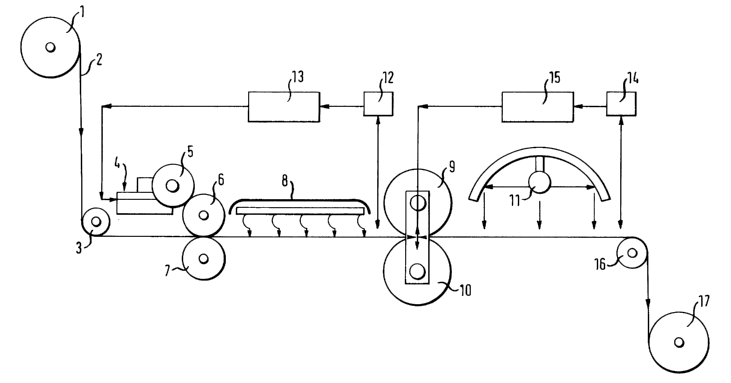
The plant represented in Fig. 1 comprises a take-off roller 1
from which a plastic film 2, e.g. a polyester film, is with-
drawn with a width of about 1 m and a thickness of 50 um.
Upon deflection about a deflection roller 3, the tape 2 is
CA 02377537 2001-12-17
_ g _
passed between a coating roller 6 and a counter-roller 7. The
coating roller 6 applies a sol-gel layer with a thickness of
about 1 um to the tape. The sol-gel is contained in a reser-
voir 4 in which a cup roller 5 is immersed, which transfers
the adhering sol-gel to the coating roller 6. The application
of a layer according to this principle is basically known
from the printing industry and will therefore not be ex-
plained in detail. other known coating methods are also ap-
plicable.
The coated tape subsequently passes through a drying station
8, in which the solvent is at least largely removed by sup-
plying heat, e.g. by infrared irradiation. At the outlet of
the drying station 8, the layer thickness of the dried, but
still embossable coating is measured by means of the indi-
cated interferometric film thickness gauge 12, whose output
signal is fed into a controller 13, which in a manner known
per se intervenes in the coating station at a suitable point,
in order to keep the layer thickness at the desired value.
Subsequently, the coated embossable tape can be wound up and
be provided for further use (not represented). Instead, the
coated tape can immediately be supplied to an embossing sta-
tion, as represented. Said embossing station comprises an em-
bossing roller 9, whose outer periphery is formed by a die
which bears the negative of the surface structure to be gen-
erated in the coating of the tape. Opposite the embossing
roller 9 a pressure roller 10 is disposed. The embossing sta-
tion is followed by a curing station 11, which may in par-
ticular consist of one or more UV light sources, which initi-
ate the radiation crosslinkage of the photopolymer contained
in the coating. Behind the curing station 11, the depth of
the pits is measured via the interferometric pit depth gauge
14, whose output signal is supplied to a controller 15, which
in dependence on the result of the comparison of the actual
value with a desired value changes the pressure of the em-
bossing roller 9 towards maintaining the desired value. Be-
CA 02377537 2001-12-17
- 10 -
hind a deflection roller 16, the tape provided with the sur-
face structure is either wound up on a wind-up roller 17 for
further use or processed. The processing not represented here
includes the punching of the blanks on the tape 2, the simul-
taneous or future punching of the central hole, if necessary
a metallizing operation, applying a protective lacquer or
laminating a protective film and mounting an adapter, which
may for instance comprise an inner ring and an outer ring and
which lifts the storage medium produced, which may be consid-
erably thinner than a conventional CD or CD-ROM, into the
reading or autofocus plane of a usual disk drive or reading
device.
In a considerably magnified representation, Fig. 2 shows a
section through a first embodiment of a storage medium corre-
sponding to a blank punched out of the coated tape 2 of Fig.
1. The storage medium comprises a polyester film 20, which by
means of the plant as shown in Fig. 1 has been provided with
a sol-gel layer 21 (alternatively with a layer of a photo-
polymer), whose side facing away from the polyester film 20
has embossed pits such as 21a. The layer 21 can have a re-
fractive index n of e.g. 1.5. By methods known per se, this
information-bearing side has been provided with a metalliza-
tion 22 (cf. Fig. 2a) and finally with a protective lacquer
23. The reading beam 24 reads out the sequence of embossed
pits and lands as in a conventional CD or CD-ROM.
Fig. 3 shows a section through a second embodiment of the
storage medium. On the polyester film 20 a layer 26 of a
Ti02-based sol-gel is provided. The index of refraction of
this layer may be in the range between 2 and 2.5. Therefore,
the reflectivity of the layer 26 is so great that the addi-
tional metallization layer 21 of Fig. 2 can be omitted in
this embodiment. In particular when this storage medium is
read out only once, in order to copy its contents onto the
fixed disk of a computer, the protective lacquer layer 23,
CA 02377537 2001-12-17
- 11 -
which is present in the embodiment as shown in Fig. 2, is su-
perfluous. Instead, the surface to be read out by means of
the reading beam 24 can merely be covered by an adhesion film
(not represented), which is simply peeled off before insert-
ing the storage medium into the reading device or disk drive.
Since the storage medium in accordance with the invention is
considerably thinner than a conventional CD or CD-ROM, an
adapter is recommendable for reading out, which adapter moves
the surface of the storage medium to be read out to about the
same plane in which the surface of a CD or CD-ROM to be read
out would be disposed, once the storage medium has been in-
serted in the disk drive.
Fig. 4 shows a section of a suitable, schematically simpli-
fied adapter. It comprises a generally circular carrier plate
30 of plastics, which has a central hole 31 with the diameter
of the central hole of a CD in an inner ring 32 protruding on
the future read-out side. This inner ring serves to center
the film-like storage medium 33, for instance of the struc-
ture explained with reference to Figs. 2 and 3. At its outer
periphery, the storage medium is fixed by an outer ring 34.
The thickness of the outer ring 34 and the thickness of the
inner ring 32 are dimensioned such that upon inserting the
adapter into the tray of a disk drive, the film-like storage
medium 33, to be more precise its surface to be read out, is
disposed at that level at which there would also be disposed
the information-bearing surface of a CD or CD-ROM, which is
covered by a polycarbonate layer.