Note: Descriptions are shown in the official language in which they were submitted.
CA 02377956 2001-12-28
WO 01/01180 1 PCT/SE00/01294
OPTOMODULE
FIELD OF INVENTION
The present invention relates to a plastic-encapsulated
optomodule as defined in the preamble of Claim 1.
DESCRIPTION OF THE BACKGROUND ART
Optomodules intended for telecommunications application for
instance are normally encapsulated in hermetic metal capsules
and are provided with a pigtail for making the optical
connection. In order to be able to widen the use of optical
signal transmissions it must be possible to produce components
and connectors at lower costs than at present, and also to
reduce the cost of mounting these components. One of the
primary reasons for such high component costs is because of the
extremely high mechanical precision that is required in
aligning an optoelectric component with a wavequide, such as an
optical fibre, and in aligning a waveguide in one component
with another waveguide.
Plastic encapsulation, transfer moulding, of optomodules
reduces production costs. In present day technology, a plastic
capsule that includes optoelectrical components can either be
provided with a fibre pigtail of varying length that consists
of an optical fibre which extends out from within the
component, or a device that is integrated in a capsule wall.
SE 9701833 describes a plastic encapsulated optomodule which
includes an integrated optical device.
CA 02377956 2001-12-28
WO 01/01180 2 PCT/SE00/01294
One problem encountered in the manufacture of plastic
encapsulated optomodules, particularly injection moulded
modules, that include an optical device integrated in the
capsule wall is that the device shall be aligned and fixed in
the capsule moulding tool.
SUMMARY OF THE INVENTION
The object of the present invention is to eliminate or at least
reduce this problem.
This object is achieved by the present invention with a plastic
encapsulated optomodule according to the characterizing clause
of Claim 1.
One advantage afforded by the present invention is that no sub-
module is required for the optoelectrical component.
Another advantage is that the optoelectrical component can be
readily constructed, manufactured and tested relatively
inexpensively.
Still another advantage is that the plastic encapsulated
optomodule requires little room on a circuit board.
Another advantage is that the present invention the manufacture
of new and re-constructed optomodules is facilitated through
the medium of a modular construction procedure .
The invention will now be described in more detail with
reference to preferred embodiments thereof and also with
reference to the accompanying drawings.
CA 02377956 2001-12-28
WO 01/01180 3 PCT/SE00/01294
BRIEF DESCRIPTION OF THE DRAWINGS
Figure 1 illustrates an embodiment of a leadframe included in
the invention.
Figure 2 illustrates an embodiment of electric components that
include a ceramic carrier, ASIC and passive components, in
accordance with the invention.
Figure 3 illustrates an embodiment of an optohybrid that
includes an optoelectrical component and an optodevice, in
accordance with the invention.
Figure 4a illustrates from above one embodiment of a plastic
encapsulated optomodule having an integrated optical interface
in accordance with the invention.
Figure 4b is a side view of one embodiment of a plastic
encapsulated optomodule having an integrated optical interface
in accordance with the invention.
Figure 5 is an overview of the placement of the leadframe, the
electric components and the optohybrid in an injection moulding
cavity.
Figure 6a illustrates from above the alignment of the
optodevice with the leadframe, in accordance with a first
embodiment.
Figure 6b is a side view illustrating alignment of the
optodevice with the leadframe in accordance with a first
embodiment.
CA 02377956 2001-12-28
WO 01/01180 4 PCT/SE00/01294
Figure 7a illustrates from above alignment of the optodevice
with the leadframe in accordance with a second embodiment.
Figure 7b is a side view illustrating alignment of the
optodevice with the leadframe in accordance with a second
embodiment.
Figure 8a illustrates from above alignment of the optodevice
with the leadframe in accordance with a third embodiment.
Figure 8b is a side view illustrating alignment of the
optodevice with the leadframe in accordance with a third
embodiment.
Figure 9a shows how the leadframes can be arranged relative to
one another during encapsulation in accordance with a first
embodiment .
Figure 9b shows how the leadframes can be arranged relative to
one another during encapsulation in accordance with a second
embodiment.
DESCRIPTION OF PREFERRED EMBODIMENTS
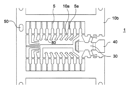
Figure 1 illustrates an embodiment of an inventive leadframe
included in a plastic encapsulated optomodule. The leadframe 1
includes a first and a second support device 10a and 10b, which
function to fixate different parts of the leadframe 1, for
instance leads 5, prior to encapsulation. The second support
device includes alignment elements 50 for aligning .the
leadframe in an encapsulating mould cavity.
CA 02377956 2001-12-28
WO 01/01180 5 PCT/SE00/01294
The leadframe includes a first part 20 which is connected to
earth via at least one earth lead 5a. The first part functions,
among other things, as a support for an electric component 1A
(see Figure 2) together with electric contact surfaces 80 at
the ends of the leads 5 and 5a.
A second part 30 functions to support an optoelectric component
2 included in an optohybrid 1B. A third part 40 functions to
support, fix and align an optodevice 3 included in said
optohybrid 1B. The electric component and the optoelectric
component may be interconnected electrically via bonding wires.
The electric component 1A is shown in Figure 2, from which it
will be seen that the electric component 1A of this embodiment
includes a ceramic carrier 9 which carries an electrically
conductive pattern 6, electrical connection surfaces 7 and an
ASIC 8 (Application Specific Integrated Circuit). The
connection surfaces 7 are connected to electric contact
surfaces 80 at the end of the lead 5. The electric component
can be surface soldered or glued to the electric contact
surfaces 80 disposed on the end of respective leads 5 and 5a.
The particular configuration of the contact surfaces 80 also
has the added function of preventing the leads from being
pulled out of the capsule. The ASIC may alternatively be
arranged directly on said first part 20 and connected
electrically to the leads with the aid of bonding wires.
Figure 3 illustrates a so-called optohybrid 1B. The optohybrid
includes an optoelectrical component 2 and an optodevice 3. The
optoelectrical component 2 includes a laser 2a to which one or
more optical waveguides 4 are connected. The optical waveguide
CA 02377956 2001-12-28
WO 01/01180 ( PCT/SE00/01294
or waveguides 4 terminates/terminate in a connecting interface
3b on said optodevice 3. The optodevice 3 includes a flange 3a.
Figures 4a and 4b illustrate the plastic encapsulated
optomodule 100. The leads 5 in the leadframe and the optodevice
protrude out from the capsules 60 in the plastic encapsulated
optomodule 100.
Figure 5 is an overview illustrating the arrangement of the
leadframe, on which said optohybrid 1B and said electric
component 1A are provided, is positioned in a mould cavity 70
for plastic encapsulation by means of transfer moulding. The
mould cavity 70 terminates inwardly of the leadframe support
devices, so as to enable these devices to be removed from the
leads 5 and 5a subsequent to encapsulation. The mould cavity 70
includes an opening for accommodating the optodevice 3. A mould
tool or die defining said mould cavity is adapted so that the
gap between the optodevice and the optodevice-accommodating
opening is restricted to some few tens of a micrometer. This
prevents plastic from penetrating between the optodevice and
the recess which accommodates the optodevice in the mould tool.
Figures 6a and 6b are enlarged views of the second and third
leadframe parts 30 and 40. Figure 6b is a sectional view taken
on the line A-A in Figure 6a. The optodevice 3 and the
optoelectric component are arranged in different planes in the
leadframe 1. This positions the waveguides 4 correctly between
the optodevice 3 and the optoelectric component 2. Tabs 45 are
folded-up from the leadframe on the third part 40 of said
leadframe 1 where the optodevice 3 is arranged. These tabs are
arranged to partially embrace the optodevice 3 such as to
fixate said device and align it in a direction orthogonal to
CA 02377956 2001-12-28
WO 01/01180 7 PCT/SE00/01294
the longitudinal direction of the waveguides 4. The tabs 45 are
also arranged to fixate and align the optodevice 3 in a
direction parallel with the waveguides 4, by virtue of said
tabs being fixed against an edge of a flange 3a on the
optodevice 3.
Figures 7 and 7a illustrate another embodiment for aligning and
fixating the optodevice with the aid of alignment elements
provided on the leadframe. In this embodiment, the third part
of the leadframe includes a recess whose position, shape and
size conform to those of the flange 3a provided on the
optodevice 3. When the flange is received in the recess, the
device will be fixated in a direction parallel with an
orthogonal to the waveguides 4 disposed between the optodevice
3 and the optoelectric component 2. As with the earlier
described embodiment, the third and the second leadframe parts
40 and 30 respectively are disposed in different planes such as
to position the waveguides 4 correctly between the optoelectric
component 2 and the optodevice 3.
Figure 8 illustrates another embodiment for aligning and
fixating the optodevice with the aid of alignment elements
provided on the leadframe 1. In this embodiment, the optodevice
3 is arranged on the third leadframe part 40, which is on a
lower level than the remainder of the leadframe. Two tabs 47a
and 47b are provided on a respective side of the third
leadframe part 40 and function to fixate the optodevice 3 in a
plane above said third leadframe part, in a direction
orthogonal to the longitudinal direction of the waveguides 4.
The tabs 47a and 47b include recesses whose shape and size
conform to the shape and size of the flange on the optodevice
CA 02377956 2001-12-28
WO 01/01180 8 PCT/SE00/01294
3, such as to fixate the optodevice also in a direction
parallel to the longitudinal direction of the waveguides 4.
Figures 9a and 9b illustrate respective methods of
interconnecting the leadframes during manufacture. The
leadframes are interconnected resiliently via V-shaped
resilient elements 80a or inclined spring elements 80b. This
enables the positioning tolerance requirement between
individual leadframes to be reduced.
It will be understood that the invention is not restricted to
the aforedescribed and illustrated exemplifying embodiments
thereof and that modifications can be made within the scope of
the following claims.