Note: Descriptions are shown in the official language in which they were submitted.
~u
A Multi-Functional Optical Switch And Its Method of Manufacture
GOVERNMENT RIGHTS IN THE INVENTION
The invention was made with Government support under Agreement No.
DASG60-98-M0158, awarded by the Ballistic Missile Defense Organization, U.S.
Department of Defense. Accordingly, the government may have certain rights in
the
invention.
TECHNICAL FIELD OF THE INVENTION.
The present invention pertains to a multifunctional optical switch that can be
employed inter alia as an optical wavelength division multiplexer, optical
wavelength
division demultiplexer, optical add-drop multiplexer and/or optical inter-
connect
device. The invention further provides novel methods of manufacturing the
optical
switch. The optical switch can comprise a single layer, and optimally includes
a
plurality of layers which each comprise an optical nonlinear second-order
polymer.
The optical nonlinear second-order polymer present in each layer preferably
differs
from that present in any other layer in terms of its absorption maximum (i.e.,
due to
possession of different chromophores).
~ BACKGROUND OF THE INVENTION
The new century heralds an unprecedented demand for ability to transport and
process large amounts of information. The incredible growth in demand for
Internet
resources and the constraints of bandwidth are but just two of the factors
that compel
the telecommunications industry to p»rsue less expensive and more efficient
options
inthe form of "all-optical" networks (as well as networks that may not solely
comprise, but do include, optical components).
For industries to meet such demand, fuxther development and improvement of
optoelectronic components {curaently bulky and expensive) is necessary. In
particular,
it will be necessary to: (i) reduce the size of tl-.e optical components; {ii)
increase the
number of channels on a given optical fiber end {iii) simplify the fabrication
process
'.';;~ "~,~_r~ ~HEE:~
3 ;. ,-
CA 02378130 2002-O1-09'
CA 02378130 2002-O1-09
WO 01/06305 PCT/US00/19921
to reduce costs. In addition, higher and higher transmission bit-rates of data
are
needed to expand the capability Of CLIrreIlt fiber communication channels.
Wavelength division multiplexers (WDMs) have become one of the hottest
commodity items in lightwave applications today since they allow multiple
wavelengths to be used as channels to transmit data within a single optical
fiber.
WDMs traditionally are based on inorganic materials. However, organic
materials,
namely polymeric materials, have recently reached a performance maturity to
compete
with these inorganic optical materials. Such materials exhibit physical and
chemical
"flexibility", and, for instance, can be relatively easily chemically modified
to suit
specific applications. This flexibility of polymeric materials makes possible,
among
other things, rapid cycles of material design, preparation, testing, and
redesign.
Organic polymeric materials are readily fabricated into integrated optical
circuitry,
which contributes to lower costs of manufacture. Polymer-based devices could
ultimately be mass-produced using simple printing processes. Moreover, organic
polymers provide a large inventory of photonic materials that can have a low
dielectric
constant. Certain of the polymers show high stability and optical
nonlinearity.
In the 1990s, polymer-based interferometers and other polymer-based devices
generated great interest (Girton et al. "Electrooptic Polymer Mach-Zehnder
Modulator." In ACS Symposium Series 601, Polymers for Second-Order Nonlinear
2o Optics (Washington D.C. 1995), 456-468). Polymeric materials have recently
emerged as materials for use in optical applications (Keil, "Realization of IO-
Polymer-Components and present State in Polymer Technology" In Integrated
Optics afid Micro-Optics With Polymers, (Stuttgart-Leipzig: B.G. Teubner
Verlagsgesellscaft, 1993), 273; Ito et al., eds., Polymeric Materials for
Microelectronics Applications, ACS Symposium Series 579 (Washington, DC:
American Chemical Society, 1991 ); Lindsay et al., eds., Polymers for Second
Order
No~zlinear Optics, ACS Symposium Series 601 (Wash., DC: American Chemical
Society, 1995), pp. 1, 11 l, 130, 158, 172, 374, 381; Edelman et al., eds.
Among the more recently developed polymeric materials are polyimides that
3o have been shown to have superior optical and physical characteristics. In
particular,
certain polyimides show thermal stability, as well as high optical
nonlinearity (as
reflected in their r33 values) (Lindsay et al., supra). The company Akzo Nobel
uses
polymers to make optical switches. Similarly, the company Lightwave has
combined
SUBSTffUTE SHEET (RULE26)
CA 02378130 2002-O1-09
WO 01/06305 PCT/US00/19921
optical design with a polymer-materials technology and semiconductor
techniques to
make waveguide structures directly on a wafer where the silicon acts as a
platform
only. Lightwave uses a polyimide polymer having a low dielectric constant and
high
temperature stability and uses heat to change the refractive index (i.e., the
polymers
are thennooptic polymers). The material made by Lightwave acts as an optical
pipe,
and theoretically could be made optically active by applying a voltage across
the
material to change the index of refraction. Then the light can be modulated or
switched from one path to another, or just modulated at high speeds. Despite
these
advances, considerable advances in the optics field still need to be made to
meet the
l0 recent demands of the telecommunications industry. For instance, devices
constructed
to date are single-layer devices, and/or are planar (i.e., the switching
occurs in one
plane to adjacent waveguides).
Thus, the present invention provides a novel device, i.e., an optical switch,
that
can perform several critical tasks for the telecommunications industry - e.g.,
wavelength division multiplexing, wavelength division demultiplexing,
performance
as an add/drop filter and/or interconnect device. The present invention
further
provides an optical waveguide. The switches and waveguide according to the
invention conceivably can be manufactured more easily and at less than the
cost of the
silicon-based devices due to novel means for their production, as further
described
herein. These and other objects and advantages of the present invention, as
well as
additional inventive features, will be apparent from the following description
of the
invention provided herein.
BRIEF SUMMARY OF THE INVENTION
The present invention pertains to a multifunctional optical switch, and novel
methods for its manufacture. The optical switch can comprise a single layer,
and
optimally comprises a plurality of layers (i.e., at least two layers,
preferably which are
stacked), which desirably each comprise an optical nonlinear second-order
polymer.
The optical nonlinear second-order polymer present in each layer preferably
differs
from that present in any other layer in terms of its light absorption maximum.
The
optical switch according to the invention desirably can be employed as an
optical
wavelength division multiplexes, wavelength division demultiplexer, add-drop
multiplexes and/or inter-connect device, among other things. Other uses of and
SI~STITUTE SHEEP (RULE2fi)
CA 02378130 2002-O1-09
WO 01/06305 PCT/US00/19921
4
devices according to the optical switch (and the optical waveguide) of the
invention
would be apparent to one skilled in the art.
BRIEF DESCRIPTION OF THE FIGURES
Figure 1 depicts the chemical stmcture of polyimide-alkoxy sulfone diazo.
Svmhol: n, ranging from about 20 to about 600.
Figure 2 depicts the chemical structure of polyimide-dialkyl amino vitro azo.
Svmhol: n, ranging from about 20 to about 600.
Figure 3 depicts the chemical structure of polyimide-dialkyl amino vitro
1o diazo. Svmbol: n, ranging from about 20 to about 600.
Figure 4 shows the absorption spectra in terms of arbitrary absorbance units
(0
to 1.8) at an applied wavelength (250 to 800 nm) of three second-order
nonlinear
optical polyimides having different pendant chromophores - i.e., sulfone diazo
(Mordant Orange 10) chromophore present in a polyimide or poly(methyl
methacrylate) host matrix ("A" peak), dialkyl amino vitro azo present in
polyimide-
dialkyl amino vitro azo ("B" peak), and dialkyl amino vitro diazo present in
polyimide-dialkyl amino vitro diazo ("C" peak). For this figure, three
different
absorbences are superimposed. The absorbances are obtained from different
thickness
films and do not correspond to scale.
2o Figure 5 depicts the chemical structure of polyamic acid doped with a
sulfone-
diazo chromophore. Svmbol: n, ranging from about 20 to about 600.
Figure 6 is a diagram of a buffered waveguide and the corresponding differing
refractive indices n,, n2, and n3, that define each layer.
Figure 7 is a diagram showing a preferred apparatus to be employed for
waveguide fabrication by a direct laser writing technique. Symbol: 10, sample;
20, X-
Y stage; 30, optical table; 40, nitrogen hood; 50, corona discharge; 60, high
voltage
supply; 70, laser; 80, laser beam; 90, lens; 100, mirror; 110, beam monitor;
120,
computer.
Figure 8 depicts chromophore alignment of polyimide-dialkyl amino vitro
3o diazo, which is measured by in situ second harmonic generation (SHG;
arbitrary units
from 0 to 2.0) at room temperature over the course of 2000 seconds, with the
onset
("Corona ON") and termination ("Corona OFF") of corona discharge depicted.
SU$STITUTE SHEET (RULE26)
CA 02378130 2002-O1-09
WO 01/06305 PCT/US00/19921
Figure 9 is a diagram showing another preferred apparatus to be employed for
waveguide fabrication by a direct laser writing technique. S'ombol: 10,
sample; 20, X-
Y stage; 30, optical table; 70, laser; 80, laser beam; 85, half wave plate;
90, lens; 100,
mirror; I 10, beam monitor; 120, computer.
Figure 10 depicts holographic grating formation using two overlapping laser
beams which intersect at an angle a in the polymeric waveguide material. The
relationship between angle of incidence in the laser beams (a) and other
geometrical
parameters can be solved geometrically according to Figure 10, where h is the
distance between the beam sputter (130) and the sample (140), b is the
distance
to between the mirror (100) and the beam splitter (130) and (3 is the angle
between b and
h as shown in Figure 10. Symbols: 80, laser beam; 100, mirror; 130, beam
splitter;
140, polymeric material.
Figure 11 shows photobleaching steps for waveguide fabrication and
subsequent grating formation with use of laser beams. Symbols: 80, laser beam;
140,
polymeric material; 150 metallic (e.g., quartz) mask; 160, irradiation; 170,
unbleached
waveguide; 180, bleached polymeric material; 190, grating formation.
Figure 12 shows parameters for single mode guiding in a rib waveguide
where "h", "w", and "t" are, respectively, the height of the non-bleached
portion of
the polymer layer, the width of the non-bleached portion of the polymer layer,
and the
2o height of the bleached portion of the polymer layer. Symbols: 140,
polymeric
material; 170, unbleached waveguide; 180, bleached polymeric material; 250,
solid
support.
Figure 13 diagrams a passive three-layer multiplexer that consists of two
waveguides connected by a holographically bleached or "surface relief "
grating.
Symbol: n, and n~ are the refractive indices of separate 2°-NLO
polymers present on
independent waveguides; n2 is the refractive index of buffer; spiral, Braggs-
Grating;
7~1 and 7~2, wavelengths. The direction of light propagation of ~,l in layer
n~ is
dependent on the spacing (or pitch) of the grating in n~.
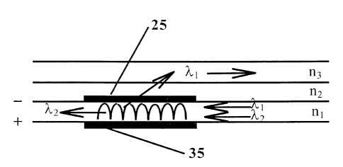
Figure 14 diagrams an active three-layer device where n,, and n~ are the
3o refractive indices of different second-order nonlinear optical polymers
(e.g.,
polyimide-alkoxy sulfone diazo (Mordant Orange 10), polyimide-dialkyl amino
nitro
azo, and/or polyimide-dialkyl amino nitro diazo), n2 is the refractive index
of the
sussrrrur~ s~~r ~u~2s~
CA 02378130 2002-O1-09
WO 01/06305 PCT/US00/19921
6
buffer layer, and the refractive index can be changed by applying an electric
field
across the waveguide. Symbols: 25, top electrode (preferably transparent such
as an
ITO electrode or a very thin metal); 35, bottom electrode; 7~1 and a~2,
wavelengths;
spiral, Braggs-Grating; +/-, applied electric field. The direction of light
propagation
of ~~1 in layer n; is dependent on the grating spacing and the applied voltage
in n,.
Figure 15 diagrams a double grating "resonance matched" multiplexer, where
n, and n; are the refractive indices of different second-order nonlinear
optical
polymers present in the layers (e.g., polyimide-alkoxy sulfone diazo (mordant
Orange
10), polyimide-dialkyl amino vitro azo, and/or polyimide-dialkyl amino vitro
diazo)
to and n~ is the refactive index of a buffer layer. Symbols: 25, top electrode
preferably
transparent such as an ITO electrode, or a very thin metal); 35, bottom
electrode ~,l
and 7~2, wavelengths; spiral, Braggs-Grating; +/-, applied electric field. The
direction
of light propagation of 7~1 in layer n~ is dependent on the position of the
grating in n,
the spacing of grating in n, and n~ and the applied voltage in n,.
I S Figures 16A-B show an illustrative embodiment of the basic device
configuration shown schematically in Figure I1. With the top view depicted in
Figure 16A, and the side view depicted in Figure 16B. Symbols: 25, top
electrode
preferably transparent such as an ITO electrode, or a very thin metal); 35,
bottom
electrode ~.l and )~2, wavelengths; spiral, Braggs-Grating; +/-, applied
electric field;
2o 250, solid support. The direction of light propagation of 7~1 in layer n3
is dependent
on the spacing of the grating and applied voltage in n,.
Figure 17 depicts a sample 4 x 4 multiplexer/demultiplexer and cross-connect
device according to the invention. Symbols: 200, enclosure box; 210, optical
circuit
board; 220, electrical connections; 230, input optical fibers; 240, output
optical fibers.
DETAILED DESCRIPTION OF THE INVENTION
The invention pertains to a multifunctional optical switch that, among other
things, desirably can function as an optical wavelength division multiplexer,
optical
wavelength division demultiplexer, optical add-drop multiplexer and/or optical
inter-
3o connect device. In particular, the invention pertains to an optical device,
particularly
an optical frequency dispersive device, such as an optical multiplexer or
optical
demultiplexer, which preferably receives light from one or more input
waveguides and
SUBSTITUTE SHEET (RULE26)
CA 02378130 2002-O1-09
WO 01/06305 PCT/US00/19921
disperses it according to frequency to one or more output waveguides. The
present
invention also optimally pertains to an optical add/drop multiplexes and to an
inter-
connect device.
According to the invention, preferably a "device" includes any single
preferred
entity as set forth herein (e.g., including, in particular, a waveguide), or
any
combination of elements (e.g., optical switch, optical wavelength division
multiplexes, optical wavelength division demultiplexer, optical add-drop
multiplexes,
optical inter-connect device and the like) either alone, or, in a higher level
of
organization (e.g., present in a system or subsystem such as a board or
motherboard).
to Preferably these entities are employed in optical communication systems,
although
each may exist in any combination, or independently, or as part of a
communications
system or other system that is other than predominantly optical (i.e., a mix
of optical
and nonoptical systems). Desirably a device according to the invention is
optically
active (as further described herein), although passive devices are also
contemplated by
and preferred according to the invention. However, one unifying feature of all
the
elements of the invention is their incorporation of a second-order nonlinear
optical
(2°-NLO) polymer, or a polymer having the desirable properties set
forth herein, as
further described below.
Certain standard terms are employed in describing the invention. Illustrative
2o definitions of these terms are set out below, and in the Examples which
follow.
Should there be any term that is left undefined, or any possible ambiguity in
the
meaning of a term, the broadest possible definition known in the
optics/electronics
fields that is consistent with the scope and goals of the invention is to be
applied.
Also, like numbering is used for the same components in each of the Figures
and in
the descriptive text.
The expression "optical communication system" or "optical system" as used
herein refers to any system which employs optical signals to convey
information
across an optical waveguide medium. Such optical systems include, but are not
limited to, telecommunications systems, cable television systems, local area
networks
3o (LANs), and the like.
A "waveguide" is an entity of material boundaries or structures for guiding
electromagnetic waves. More specifically, a waveguide is an optical waveguide,
or
SUBSTITUTE SHfEf (RULE26~
CA 02378130 2002-O1-09
WO 01/06305 PCT/LTS00/19921
any stricture capable of guiding optical power (i.e., carrying one or more
optical
signals).
A "second-order nonlinear optical" (2°-NLO) polymer is a polymer
that is
optically active -- i.e., its index of refraction changes due to an applied
electric field,
and the change is proportional to the square of the applied electric field.
Preferably
according to the invention, a 2°-NLO polymer is obtained by the
incorporation into a
polymer backbone of a chromophore having 2°-NLO characteristics, and/or
which
exhibits those characteristics when present in the polymer backbone.
According to the invention, a waveguide preferably is comprised of a layer of
2°-NLO polymer. Desirably the waveguide is flanked on at least one side
by a solid
support capable of supporting the waveguide, wherein the solid support can be
any
appropriate material, e.g., glass, plastic, metal, and the like. The solid
support need
not be entirely rigid (although completely rigid materials can be employed),
but can
have some amount of flexibility. Preferably the waveguide also is flanked on
at least
one side by cladding. Whenever a solid support is employed to support the
waveguide, the support must not directly contact the waveguide, but must be
separated
from the waveguide by cladding. It is necessary for proper functioning of the
waveguide that the index of refraction in any layer that directly contacts the
waveguide (i.e., on one or more sides, and preferably on all sides) is less
than the
index of refraction in the waveguide itself. Accordingly,cladding can include
one or
more layers of any appropriate material that has an index of refraction that
is less than
the index of refraction in the waveguide itself, such as 2°-NLO
polymer, glass, plastic,
silica, or other appropriate material, and further can include a buffer (e.g.,
as set out in
Figure 6, and in other figures). According to the invention, "a buffer" is an
optical
buffer, i.e., a medium that does not exhibit any optical activity or optical
nonlinearity
with lower refractive index. Optionally according to the invention, the
cladding layers
can be conductive as described in U.S. Patent 5,887,116 (incorporated by
reference).
The index of refraction in each layer (e.g., of a waveguide or of an optical
switch) is impacted by the chromophore concentration, the nature of the
chromophore,
and the nature of the polymer backbone. Of course, these parameters can easily
be
optimized by one skilled in the art. Desirably, the waveguide can comprise any
part of
a circuit or optical device (i.e., an optical switch).
SI~STITUTE SHEET (RULE2f~
CA 02378130 2002-O1-09
WO 01/06305 PCT/US00/19921
As indicated previously, to function as a waveguide, the index of refraction
in
any layer surrounding the waveguide must be less than the index of refraction
in the
waveguide itself. This difference in refractive index between the waveguide
itself
and any adjacent layer (i.e., "4n" in Example 2) preferably is equal to or
greater than
0.001, and desirably is no more than 0.1. However, with alternate thicknesses
of
waveguide, it is conceivable that the range of differences may be slightly
broader.
Such alternates are contemplated by the present invention.
Thus, desirably the present invention contemplates an "asymmetric
waveguide" and a "symmetric waveguide". In the case of an asymmetric
waveguide,
to i.e., comprised of a waveguide surrounded by an upper and lower cladding
layer, the
refractive indices of the upper and lower layers are not equal to each other,
and are
less than the refractive index of the waveguide. In the case of a symmetric
waveguide,
i.e., comprised of a waveguide surrounded by an upper and lower cladding
layer, the
refractive indices of the upper and lower layers are equal to each other, and
are less
than the refractive index of the waveguide. This is further described in
Example 2.
An "optical switch" is a device that is capable of changing the path of light
from one waveguide to another (e.g., a multiplexer/demultiplexer, add/drop
multiplexer, and/or interconnect), or from one waveguide to air or cladding
(e.g., as a
drop multiplexer, and/or connected to a detection device).
2o An "optical multiplexer" is a device which combines a plurality of optical
signals having different wavelengths in a single optical fiber on the
transmitting side.
An "optical demultiplexer" is a device which separates a multiplexed signal
into a
plurality of optical signals of different wavelengths on the receiving side.
Essentially,
an optical multiplexer is an optical demultiplexer run in reverse, and vice
versa.
In particular, an optical "wavelength division multiplexer" ("WDM") is a
system that employs WDM signals consisting of a number of different wavelength
optical signals (known as "carrier signals" or "channels") to transmit
information on
optical fiber or in an optical waveguide. In a WDM system, optical signal
channels
are generated, multiplexed (i.e., added together) to form an optical signal
comprised
of the individual optical signal channels, transmitted over a single
waveguide, and
demultiplexed (i.e., separaed) such that each channel wavelength is
individually
routed to a designated receiver. The various channels within a WDM signal can
be
SUBSTITUTE SHEEP ~RULE28)
CA 02378130 2002-O1-09
WO 01/06305 PCT/US00/19921
distinguished by their optical wavelength and/or their optical frequency, with
these
terms being used interchangeably herein as features of the optical signal.
An optical "add/drop multiplexer" (OADM) is a device which facilitates the
addition (i.e., add multiplexing) and/or subtraction (i.e., drop multiplexing)
of
5 particular carrier signals to or from the WDM signal at different locations
on an
optical network. For instance, such routing can occur when optical channels
are sent
to or withdrawn from an optical transmission line, e.g., for sending optical
channels
between a terminal and an optical bus, or for routing long distance
telecommunications traffic to individual cities, or for other uses. An OADM is
thus
10 essentially just a variation of a WDM such as is known in the art.
An "optical interconnect" (OIC) or "optical cross-connect" (OXC) provides
routing of signal at the optical (wavelength) level. An OIC/OXC can route a
signal
from point A to point B or C. It provides wavelength management on a number of
incoming and outgoing fibers, and optimally can contribute to optical grooming
and
restoration capabilities.
An "active" device according to the invention is one which responds to an
applied electric field. An active device must contain at least one grating,
but each
waveguide present in the device (i.e., in the case of a device comprised of
more than
one waveguide) need not necessarily contain a grating. In other words, with an
active
2o device, its optical properties are changed when a voltage is applied to it.
By
comparison, a "passive" device according to the invention is one that does not
change
its characteristics when a voltage is applied to it, and/or a device that
functions
without needing to apply a voltage (i.e., and to which a voltage is not
applied).
According to the invention, the electric field is generated with any
appropriate
power source (e.g., AC or DC power source), and communicated to the device or
switch by means of an electrode. The electrode used in the present invention
preferably is made of at least one of the following materials: metals such as
gold,
silver, platinum, copper, and alloys; conductive materials such carbon black,
conductive epoxy, or indium tin oxide (ITO). However, any electrode having the
3o ability to conduct charge and capable of functioning as an "electrode" as
that term is
understood in the art can be employed in the methods and devices of the
invention.
Generally, an electrode need only supply a small amount of voltage, e.g., from
0 to
S(~STITUTE SHfET (RULE26~
CA 02378130 2002-O1-09
WO 01/06305 PCT/US00/19921
about 50 volts, although in certain applications, it may be preferable to
employ a
higher voltage.
According to this invention, a "grating" is a means of separating an optical
signal. A particularly preferred grating for use in the invention is a Bragg-
Grating. A
"Bragg-Grating" is an element for selectively controlling specific wavelengths
of light
within a waveguide. A typical Bragg-Grating contains a length of waveguide
that
includes a plurality of periodic perturbations in the index of refraction,
wherein the
perturbations are substantially equally spaced along the length of the
waveguide.
These perturbations selectively reflect light having a wavelength (~,)
equivalent to
to twice the spacing (A) between the successive perturbations (i.e., 7~ =
2nP~A, where ~, is
the vacuum wavelength and net is the effective refractive index of the
propagating
mode). The light that is not selectively reflected by the Brags Grating passes
through
the grating unimpeded.
Conventional gratings such as the Fiber Bragg-Grating are typically
manufactured by using a waveguide (e.g., an optical fiber) that includes one
or more
elements in their core that are sensitive to ultraviolet light, and then
exposing the
waveguide at periodic intervals to high intensity ultraviolet light (or other
appropriate
light), e.g., from an excimer laser. Generally, the appropriate periodic
spacing of
perturbations in a grating is accomplished with use of some sort of physical
mask to
2o adjust areas exposed to the laser (e.g., a photo mask), a phase mask, or a
pair of
interfering beams (e.g., holographic techniques). Further preferred approaches
for
generation of a grating according to the invention, particularly a Bragg-
Grating, are
described below, and in the Examples which follow, as well as are illustrated
in
Figure 10. However, other means of grating generation known in the art
optionally
can be employed.
In particular, preferably the present invention provides an active Bragg-
Grating
multiplexer (desirably produced via optical waveguide writing techniques such
as
photobleaching and laser writing as further described herein), in thin layers
fabricated
from soluble, second-order nonlinear optical (2°-NLO) polymers. The
invention
3o further provides a demultiplexer, OADM, an OIC/OXC, and other active and
passive
devices. Preferably such devices according to the invention comprise a single
layer of
2°-NLO, and optimally comprise more than one layer of the 2°-
NLO, especially from
SUBSTffUTE SHfET ERULE26)
CA 02378130 2002-O1-09
WO 01/06305 PCT/US00/19921
12
two to ten layers of different 2°-NLOs, desirably from two to six
layers of different
2°-NLOs, and particularly two or three layers of different 2°-
NLOs. When more than
a single layer of 2°-NLO is present, optimally according to the
invention the layers are
"stacked" (although a side-by-side juxtaposition also can be employed).
Desirably the
s optical switch devices as described above further comprise one or more
buffer layers,
as well as other optional components (e.g., interferometer). Preferably, the
gratings)
(e.g., Bragg-Grating(s)) are present in the buffer layers) and/or the
waveguide layers)
comprised of 2°-NLOs.
Preferably the ?°-NLOs employed in the invention (or other
appropriate
to polymer) exhibit thermal and mechanical stability, and high optical non-
linearity.
Desirably the 2°-NLO does not suffer thermal decomposition until
above about
300°C. Optimally the 2°-NLO has a large electro-optic
coefficient (r3~) ranging
anywhere from between about 5 to about 40 picometer/volt (e.g., as reported in
the
literature).
15 It particularly is preferred according to the invention that the 2°-
NLO is a
polyimide, i.e., having as a "polymer backbone" poly [N, N (1,4 phenylene)-4,
4'
(hexa fluoroisopropylidene) diphthalic imide] depicted as "Z" in Structure I
below and
hereafter referred to generally as "polyimide" (although "S" and "C" present
in the
polyimide may differ, and are further described below):
Z S C
Structure I
In Structure I, the preferred structure of the 2°-NLO polymer according
to the
invention, the polymer backbone is attached to a spacer, "S", which itself is
attached
to a chromophore "C", each of which is further described below. The polyimide
according to the invention optionally can be modified or substituted if
beneficial for a
particular application, so long as such modification/substitution allows
functionality
within the spirit and scope of the invention. Alternately, instead of the
chromophore
being covalently attached to the polymer backbone, the chromophore desirably
can be
non-attached and used to dope the polymer.
SI~STITUTE SHEET (fiULE26)
CA 02378130 2002-O1-09
WO 01/06305 PCT/US00/19921
Is
In situations where it is not necessary that the polymer backbone exhibit
thermal stability above 300"C, the polymer backbone can comprise the following
polymers (or other polymers) instead of polyimide, and which have the thermal
glass
transition values (°C) indicated: Poly(methyl methacrylate), 114;
Polystyrene, 100;
Polyp-hydroxystyrene), 150; Polycarbonate, 150; Polyester, 38-130;
Polyurethane,
140; Poly(phenylene vinylene), 40; Polyquinoline, 175; Polyamide, 276;
Polyimide,
310. Thus, desirably according to the invention, these other polymers can be
employed instead of polyimide as the polymer backbone "Z".
In particular, however, preferably the polymer backbone "Z" is polyimide,
i.e.,
to having Structure II (M,y. of about 454) depicted below:
CF3 CF3
0 0
N
OH o O
Structure II
where n preferably is any number ranging from about 20 to about 600, and
desirably
ranges from about 100 to about 300. Generally it is found that longer chains
(i.e.,
where n is greater than 20) give better properties in the sense that the
chains
intertangle better. Too great of a chain length, however, deleteriously
impacts
polymer solubility.
2o It further is desirable according to the invention that the polymer
backbone "Z"
is a polyamic acid having Structure III depicted below, and which upon heating
becomes insoluble in organic solvents:
SUBSTITUTE SHEET (~ULE26)
CA 02378130 2002-O1-09
WO 01/06305 PCT/US00/19921
14
_ O O
O ~ ~ CF3 CF3
/~ n
HO~ ~ ~ ~OH
Structure III
where n preferably is any number ranging from about 20 to about 600, and
desirably
ranges from about 100 to about 300.
The spacer, "S", in Stricture I preferably is a chain of from 0 to 30 carbons
(or
other moieties, including attached moieties, such as hydrogen, and functional
groups
including but not limited to alkyl groups) which provides optimal spacing such
that
the polymer backbone is appropriately attached to, and does not interfere
with, the
l0 functionality of the chromophore ("C"). In particular, preferably the
spacer has a
length of from 1 to 10 atoms, and even more desirably, from 2 to 6 atoms.
However,
the spacer must be of sufficient length and character such that it does not
interfere
with the function of (e.g., the conjugation of) the attached chromophore, as
well as
does not interfere with the 2°-NLO properties of the polymer. A
preferred spacer
according to the invention is oxytrimethylene spacer. Other preferred spacers
are
those depicted in Figures 1-3 (shown already attached to the polymer
backbone).
With regard to the chromophore, "C," the 2°-NLOs polyimide with
chemically
attached (i.e., polyimide-alkoxy sulfone diazo) or doped sulfone diazo
(Mordant
Orange 10, purchased from Sigma-Aldrich Fine Chemicals, St. Louis, Missouri),
chromophore, polyimide-dialkylamino nitro azo, and polyimide-dialkyl amino
nitro
diazo (see, Saaedeh et al., "Polyimides with a Diazo Chromophore Exhibiting
High
Thermal Stability and Large Electrooptic Coefficients", Macromolecules, 30
(18),
5403-5407 ( 1997); Yu et al., "Novel Second-Order Nonlinear Optical, Aromatic
and
Aliphatic Polyimides Exhibiting High-Temperature Stability", Applied Plrysics
Letters, 66, 1050-1052 (1995); Yu et al., "Novel Second-Order Nonlinear
Optical
Polyimides," Society of Photooptical Instrumentation Engineers, 2527, 127-136)
are
especially preferred for use in the invention. These polyimides incorporate
the
chromophores dialkyl amino nitro azo (e.g., present in polyimide-dialkyl amino
nitro
SUBSTITUTE SHEET (RULE26~
O O
CA 02378130 2002-O1-09
WO 01/06305 PCT/US00/19921
1;
azo), sulfone diazo (e.g., present in polyimide-sulfone diazo), and dialkyl
amino vitro
diazo (e.g., present in polyimide-dialkyl amino vitro diazo). These polyimides
(as
well as other polyimides, or other polymers appropriate for optical
applications)
optimally can be modified by the incorporation of different chromophores into
the
polyimide backbone, allowing the responsiveness of the 2°-NLO to
different
wavelengths of light to differ.
Such modification of the polyimide backbone with different chromophores is
known in the art, and is described, for instance, in Marder et al., Natiti-e,
388, 845-851
( 1997). The chromophore incorporated in the polyimide can be any chromophore,
but
to desirably is a chromophore including, but not limited to: (a) the three
chromophores
previously described, and (b) those chromophores depicted in Table 1. In Table
I
below, "p" is the dipolar moment of the molecule, "(3" is the
hyperpolarizability, and
"7~" is the wavelength.
SUBSTITUTE SHEET (RULE26~
CA 02378130 2002-O1-09
WO 01/06305 PCT/US00/19921
16
Table 1
Stru Ctu re ~t (3 S 04$ ~ ma
nm
1 NMe
n=2 813 442
NOz n=3 1074 458
n n=4 1700 464
n=2 to 4
2 Mez~N ~
N~ NOz 751 480
3 NPhz~N\
N~ NOz 788 486
4 EtzN ~N\ ~
N~ NOz 996 494
NPhz~ N\
1360 526
N~ CHC(CN)z
g NPhz~N\ ~-
N~ Cz(CN)s 2776 602
7 EtzN~N ~~..//\
N~N\
N~ NOz 19000 504
Etz~N\
N~N\ -
\N~C2(CN)~ 24000
~/N
9 Me ~ ~ - ~ ~ \ 276 362
S ~ NOz
NPhz ~ ~ ~ ~ \
S ~ ~ NOz 756 458
11 NPhz ~ ~ N ' N
\ N ~/ ~ 1390 550
S ~ NOz
CH3
CH3
12 / \ NN ~ ~ N HO
'' ~ ~ - 518
HsC N
H3C
SUBSTITUTE SHEEP (RULE26)
CA 02378130 2002-O1-09
WO 01/06305 PCT/US00/19921
17
Desirably the chromophore employed in the invention has an
absorption wavelength from between about 200 nm and about 800 nm,
preferably from between about 300 nm and about 600 nm. The preferred
chromophores according to the invention also desirably have an effective cis-
traps isomerization process when excited at their absorption wavelengths.
Also, desirably the chromophores are such that polarization alone can be used
to induce alignment in the chromophores (e.g., as described in Rochon et al.,
"Optically Induced and Erased Birefringence and Dichroism in Azoaromatic
Polymers", Appl. Plrys. Lett. G0, pages 4-5 (1992); Kim et al., "Laser Induced
to Holographic Surface Relief gratings on Nonlinear Optical Polymer Films",
Appl. Phys. Lett. 66, pages 1166-1168, (1995)). Optimally this induced
alignment will be in the direction to reduce interaction with the incident
polarized light.
According to the invention, and, as further described below, a
waveguide that exhibits 2°-NLO properties can be obtained not only by
chemical conjugation of a 2°-NLO chromophore into a polymer backbone,
but
also desirably can be obtained by merely mixing a 2°-NLO chromophore
with
a polymer backbone in a process commonly known as "doping". For "doping"
it is preferable that the concentration of the chromophore be between about 3%
and about 10% of the total polymer mixture. Other variations such as would
be obvious to one skilled in the art are contemplated by the invention.
The chemical structures of certain of the preferred polyimides to be
used for the proposed device according to the invention are shown in Figures
I-3, with the corresponding absorption spectra of the corresponding polymers
being shown in Figure 4. These materials provide great flexibility in terms of
chemical modification, such modification which may be desirable in
optimizing the properties of the polymer for use in optical applications. For
instance, in dialkyl amino nitro diazo it is possible to change the electron
donor in the chromophore from nitrogen to oxygen and the electron acceptor
3o from nitro to sulfone to get the alkoxy sulfone diazo (Mordant Orange 10).
This will shift the absorption of the material from 532 nm to 386 nm as shown
in Figure 4.
S~1~U1~SHEET(RULE26)
CA 02378130 2002-O1-09
WO 01/06305 PCT/US00/19921
18
Therefore, by changing the pendant chromophore in the polyimide employed
in the different layers of the device according to the invention, the
absorption peaks
for each layer can be completely separated, or single layer devices having
different
optical properties can be obtained. Hence, inter- alicc, the invention renders
it possible
to manipulate each layer of the polymer films by using the appropriate
wavelength to
induce refractive index changes. The concentration of chromophores can be
carefully
adjusted by copolymerization to control the refractive index at the expense of
the
nonlinearity (e.g., as described in Girton et al., supra, and Keil, szepr-a).
Furthermore, with active devices, transparent electrodes can be
to incorporated in the form of transparent layers of Indium-Tin-Oxide ITO.
Under proper conditions it can form a thin film on a glass or polymer
substrate
which is electrically conductive and optically transparent in the ultraviolet
to
infrared region of the electromagnetic spectrum. It can be deposited as a thin
film layer (typically 100 nanometer thickness) using an alloy of Indium and
Tin and Oxygen atmosphere by reactive sputtering techniques. Reactive
sputtering techniques include DC, RF, and Magnetron sputtering, and are
known to those working in the field.
Taking advantage of highly efficient 2°-NLO polymers that have
large
electro-optic coefficients (e.g., the preferred polyimides depicted in Figures
1
3, or other polyimides), the driving voltage for the operation of an active
device according to the invention which incorporates such a 2°-NLO
should
also be low. The novel fabrication processes according to the invention allow
the construction of multiple levels or multiple layers on the same board.
According to the invention a "board" can be a simple glass substrate or a
silicon chip with electronic circuits or any sort of support platform for the
polymer films. The multiple levels or layers on the board are individually
processed and interconnected to other layers by various means (e.g.,
directional and grating couplers, and/or inter-connects). By constructing such
mufti-layered systems, it is possible to fabricate very dense optical
integrated
3o circuits (e.g., having more than one function, such as a combination of
interconnected circuit elements inseparably associated on or within a
continuous substrate), if so desired. A sample board according to the
invention is depicted in Figure 17.
SUBSTITUTE SHfEf (RULE26)
CA 02378130 2002-O1-09
WO 01/06305 PCT/US00/19921
19
The methods of fabricating the novel devices of the invention desirably
employ a number of novel photo-processes such as photo-induced (Rochon et
al., "Optically Induced Surface Gratings on Azoaromatic Polymer Films",
Appl. PJws. Lett., 66, pages 136-138, (1995)), or photo-induced electric-field-
assisted (Hill et al., "Reversible Optical Storage Utilizing Pulsed,
Photoinduced, Electric-field-assisted Reorientation of Asobenzenes", AppJ.
PJws. Lett. 66, pages 2156-2158, (1995)) poling (apparatus shown in Figure 5)
and photobleaching techniques (Figure 11) for writing gratings and
waveguides (Keil, supra). These processes facilitate the fabrication by
to producing waveguides using lasers at the absorption wavelength of the
2°-
NLO chromophores (e.g., typically between from about 300 nm to about 600
nm). The waveguides are unaffected by light with lowest wavelength outside
the range of their absorption, such as at communication wavelengths of from
about 1.3 to about 1.5 microns. Additionally, these processes reduce the costs
dramatically and provide an easy way to fabricate integrated optical circuits.
With use of the preferred laser writing technique, desirably a holographic
grating can be assembled with proper pitch to control the amount of out-
coupled light
with the appropriate fraction. Also, optionally the destruction of the
chromophores by
a well established photobleaching process (see, e.g., Rikken et al., "Poled
polymers
for frequency doubling of diode lasers" Proc. SPIE, vol 1337, pp 35 ( 1990))
using a
photo-masking technique that causes a reduction of the chromophores in the
material,
can be employed to produce efficient waveguides in a preferred process
according to
the invention.
Gratings on waveguides for light coupling (including the Bragg-Grating
discussed previously) have been studied for a number of years (Tamir, ed.,
"Topics in
Applied Physics: Integrated optics", Springer Verlag, Vol. 7, page 92,
(1979)), and
coupling efficiencies of 80% or more have been achieved for passive couplers
by the
proper adjustment of waveguide layers and refractive index, n, and groove
spacing of
the grating, A. Making use of the second-order nonlinearity of the waveguides,
the
refractive index, n, across the grating can be changed by applying a field
across the
waveguide. This allows the coupling efficiency of the grating to be changed or
adjusted. Such a device according to the invention provides an active grating-
coupler
that also can be employed as a light modulator, a light filter, or even a
light valve.
SUBSTITUTESHEET(RULE28~
CA 02378130 2002-O1-09
WO 01/06305 PCT/US00/19921
In particular, the present invention desirably provides a methodology to
fabricate "stacked" integrated optical circuits (i.e., circuits that are
layered one on top
of another instead of side-by-side, or in the same plane). Preferably such
circuits are
constructed using a unique laser-writing waveguide fabrication technique in
accordance with the invention. A stacked device having two or more layers
(especially
having three layers) and which has independent waveguides and gratings in each
layer
is particularly preferred according to the invention. A variety of fabrication
techniques can be employed to carry out constriction of this device, e.g.,:
(a)
preferably utilizing index anisotropy caused by photo-induced chromophore
10 orientations in 2°-NLO polymers (laser-writing) to fabricate the
waveguide and the
grating; (b) optionally utilizing the photobleaching process to fabricate the
waveguide
and the grating; and (c) optimally using a combination of these two
techniques. The
term "anisotropic" refers to a material whose electrical or optical properties
are
different for different directions of propagation or different polarizations
of a traveling
15 wave.
A device according to the invention can comprise one or more polymer layers
as depicted in Figure 6. Figure 6 diagrams a waveguide where the refractive
indices
n,, n2, and n3, are all different. The layers having these respective indices
can
comprise either air, buffer, and/or 2°-NLO. A "buffer" can be another
polymer or any
2o other material which: ( 1 ) has a lower refractive index than the guiding
layer and light
of the relevant range (i.e., range of chromophore excitation of chromophore
employed
in the device) passes through unaffected, (2) is employed to separate one
layer from
another layer or material (e.g., electrode), and (3) is noninterfering with
the optical
properties of layers above and/or below the buffer layer. Thus, a buffer layer
can act
merely as a separator and can be, for instance, a polymer such as polyimide,
where the
polymer (polyimide) does not contain any chromophor. In particular, preferably
the
buffer is polyimide, PMMA, or polystyrene that does not contain a chromophor.
An especially preferred embodiment according to the invention is the active
WDM device having the arrangement shown in Figure 14. Thus, among other
things,
3o the present invention provides for an "active" Bragg-Grating WDM. Using the
polymer with a sulfone diazo chromophore (Figure 3), in a first method, the
well
established photobleaching method desirably can be used to write both the
waveguide
and the grating (Figure 11 ). In a second method, preferably using the direct
laser-
SUBSTITUTE SHEET (RULE26~
CA 02378130 2002-O1-09
WO 01/06305 PCT/LJS00/19921
21
writing technique, waveguides and gratings in a single-layer polymer can be
constructed. Following construction of the single-layer systems, one or more
additional polymer layers optionally can be added, and a device or system
having two
or more stacked polymer layers optionally can be constructed. To construct a
second
layer, or another layer (i.e., a third, fourth, fifth or other polymer layer),
the underlying
layer or layers (e.g., the first or other layers) constructed prior to the
present layer
being applied can be protected by a UV absorbing buffer layer such as
polymethyl
methacrylate (PMMA) or, with use of laser-writing techniques, e.g., employing
a
polymer which incorporates a different chromophore causing absorption at a
different
to wavelength.
Following construction of a single layer device according to the invention,
parameters such as stability, grating-index modulation depth, surface relief
index
modulation depth, and the effect of each parameter on the resonance condition
for in
and out-coupling efficiency of the guided wave are evaluated. These parameters
15 confirm the optimal approach for fabrication of a multi-layer optical
integrated circuit
device capable of performing Wavelength Division Multiplexing (WDM), Add/Drop
Multiplexing (OADM) and/or Cross-Connect (OXC) operations. The following
accordingly is an outline of some of the physical and theoretical issues that
are
addressed in practicing and optimizing the invention (although each of the (7)
steps
2o below is not strictly necessary, just merely exemplary).
( 1 ) Determination of materials for and synthesis of the suitable material
for the
waveguide. In particular, use of 2°-NLO polymers, particularly
2°-NLO polyimides
(especially polyimide-dialkyl amino nitro azo, polyimide containing sulfone
diazo,
and polyimide-dialkyl amino nitro diazo) is preferred according to the
invention,
25 although other polymer chromophors also can be employed, e.g., as described
herein.
The proper solvents and concentrations for each material for spin-coating
uniform,
thin, films on glass substrates needs to be addressed. Generally, however,
appropriate
coating can be obtained with use of a polymer having a concentration of at
least about
300 g/1 of N-methyl pyrrole (NMP) or dimethylformamide (DMF). In general, for
3o thick, uniform films, a high boiling point solvent is desirable. Typically
according to
the invention, the polymer is prepared e.g., in powder form. Subsequently the
polymer is dissolved in a suitable solvent (e.g., NMP) and spin-coated on a
surface, or
adhered to the surface by any appropriate means known in the art. Procedures
for
SUBSTffUTE SHEET (RULE26~
CA 02378130 2002-O1-09
WO 01/06305 PCT/US00/19921
22
precipitating the polymer as a powder, washing and drying the polymer, making
a high
concentration solution (e.g., in 1 to 2 ml of solvent) and spin coating (e.g.,
onto about
a 1.5 x 1 inch surface, such as glass microscope slide) are known in the art
(see, e.g.,
Saadeh et al., snpna).
(2) Guided-wave structure design. A mathematical simulation of the guided
wave conditions of different wave guide structures applied to 2°-NLO
polymers
desirably can be performed. Such simulation optionally takes into account the
geometry and material properties such as the difference in the refractive
indexes
between poled and unpoled polymer films using the different poling methods
(laser
and corona). For fabrication of complicated circuits, this step may be
required. Any
appropriate simulation program known and available in the art can be employed
(e.g.,
the product BPM CAD, Optiwave Corp., ON, Canada; the product Beam Prop, R
Soft, Inc., NY, NY; and the product Thor/Prometheus, BBV Software BV, The
Netherlands)
(3) Construction of specialized apparatus (or modification of an existing
apparatus) for waveguide fabrication and testing. As depicted in Figure 7, a
computer
controlled precision X-Y stage apparatus is preferred for laser writing of
waveguides,
and subsequent testing of waveguides, although other means can be employed.
The
apparatus desirably can be constructed using commercially available,
programmable,
2o high-precision X-Y translation tables. Other components of the apparatus
also are
commercially available.
(4) Fabrication of waveguides using, for instance, laser-induced chromophore
alignment and photobleaching technique. Also, the same techniques desirably
can be
employed to write surface-relief gratings in the highly nonlinear polymers
with
sulfone and diazo chromophores, and to measure the nonlinearity of the
waveguide
and diffraction efficiency of the fabricated gratings from outside and through
the
waveguide.
(5) Analysis of the waveguides (e.g., to determine the effectiveness of the
laser-writing technique which induces chromophore alignment to produce index
anisotropy) and examination of the gratings, desirably by Atomic Force
Microscopy
(AFM), or other appropriate means. Also, a determination can be made of the
performance of the components fabricated with different methods such as
SUBSTITUTE SKEET (RULE~f~
CA 02378130 2002-O1-09
WO 01/06305 PCT/US00/19921
23
photobleaching as compared with photo-induced poling, to determine the optimal
means for fabrication of the components for a particular application.
(6) Fabrication of stacked waveguides using the same techniques as in (4)
above.
(7) Determining the multiplexing and coupling efficiency of the active devices
according to the invention as compared to passive devices known in the art (as
well as
prepared according to the invention). Similarly, an assessment can be made of
waveguide loss in the waveguide and through the grating of the novel devices
according to the invention. This can be done, for instance, using prism-
coupling,
to along with a near-field fiber-probe technique (which is well-known in the
art). The
measurements can be repeated for each layer present in a device according to
the
invention. This determination, of course, is done merely to optimize
components for a
particular application.
Thus, the present invention optimally provides for construction of a family of
15 components and devices, based on the uniquely designed polymer waveguides
according to the invention, which optionally combine the passive WDM of the
Bragg-
Grating with the nonlinearity of 2°-NLO polymers. In a preferred
embodiment, an
optical add-drop multiplexer is constructed which also has optical cross-
connect
properties.
20 The following Examples are by means of illustration, not limitation. Of
course, variation of these Examples in the spirit and scope of the invention
are
contemplated herein.
Example 1: Polymer Synthesis and Preparation of Wave~uide and Cladding
25 This Example describes polymer synthesis and preparation of exemplary
waveguide and cladding layers.
This Example describes the preparation of two stable cis-traps-active
2°-NLO
polymers which have separate and preferably far apart absorption peaks. The
absorption spectra of the chromophores used (i.e., sulfone diazo (Mordant
Orange 10)
3o chromophore present in a polyimide or poly(methyl methacrylate) host matrix
("A"
peak), and dialkyl amino nitro diazo present in polyimide-dialkyl amino nitro
diazo
("C" peak)) are shown in Figure 4. The materials shown in the Figure 4 are not
the
only azo dyes with appropriate properties for use in the invention. Other well-
known
SUBSTITUTE SHfET (~ULE2fi)
CA 02378130 2002-O1-09
WO 01/06305 PCT/US00/19921
24
azo dyes such as Disperse-Red exhibit similar properties (Sekkat et al., "Room-
Temperature Photoinduced Poling and Thermal Poling of a Rigid Main-Chain
Polymer with Polar Azo Dyes in the Side Chain", Chem. M~cten, 7, 142-147
(1995)).
However, the absorption peak of Disperse-Red is at 480 nm, making it
unsuitable to
use in conjunction with the material shown in Figure 4.
The chromophores are preferably chemically attached to the polymer backbone
(e.g., soluble polyimides) for better thermal stability. The nitro-diazo
chromophore
was chemically attached to the polyimide backbone to produce the polyimide-
dialkyl
amino nitro diazo polymer shown in Figure 3. Synthesis was carried out as
described
to in Saadeh et al., "Polyimides with a Diazo Chromophore Exhibiting High
Thermal
Stability and Large Electrooptic Coefficients", Macromolecules, 30, 5403-5407
( 1997).
Chromophores alternately can be physically associated with, but not
chemically attached to the polymer backbone, e.g., as wherein the polymer is
"doped"
with the chromophore of interest. Such a material, polyamic acid doped with
sulfone-
diazo chromophore is depicted in Figure 5. This material was made by mixing
sulfone-diazo chromophore with polyamic acid (purchased and used as received
from
Aldrich Chemicals) and heat-cured at about 200 °C. Sulfone-diazo
chromophore was
prepared by dissolving Mordant Orange 10 (purchased from Aldrich Chemicals),
2o which is a sodium salt, in water and adding excess amount of HCl to
precipitate the
sulfone-diazo chromophore.
For making films using polyimide-dialkyl amino nitro diazo, 300 mg of
polymer was dissolved in 6 ml of tetrachloroethane. The solution was then
filtered
with a 0.2 micron filter and the total volume was reduced to 1.7 ml. The
solution was
then spin-coated on indium-tin-oxide (ITO) substrates. Depending on the
spinning
speeds, the film thickness ranged between 2 to 5 micron.
For making films using polyamic acid doped with sulfone-diazo chromophore,
36 mg of sulfone-diazo was dissolved separately in 1 ml of N-methyl pyrrole
(NMP).
This solution was added to 0.5 gram of polyamic acid solution which has 20%
3o polymer content. To this mixture 3.5 ml of NMP was added, the solution was
filtered,
and the total volume was reduced to 1 ml. Spin-coating at 5000 rpm produced
films
about 2 to 3 micron thick. These films may then be imidized at 200 ° C
to form a hard
and insoluble film. The insolubility is necessary for mufti-layer films.
SI~STITUTE SHfET (RULE26~
CA 02378130 2002-O1-09
WO 01/06305 PCT/US00/19921
?i
Cladding also can be fabricated for the waveguides and optical switches of the
invention, e.g., to separate the waveguide from the solid support, or two
separate
independent waveguides. For fabrication of cladding, the refractive index of a
light-
guiding layer (i.e., a waveguide) must be higher than the layers above and
below it.
In particular, to fabricate a multilayer optic switch comprised of separate
waveguides
made of either polyimide-dialkyl amino nitro diazo or polyamic acid doped with
sulfone-diazo chromophore, these two guiding layers must be separated by a
cladding
layer. By imidizing pure polyamic acid, an insoluble layer with lower
refractive index
than either polyimide-dialkyl amino nitro diazo or polyamic acid doped with
sulfone-
1o diazo chromophore is formed. The structure is represented in Figure 6,
wherein in
this case, n~ and n3 are waveguides, and n2 is cladding. Optimally, but not
depicted in
Figure 6, the waveguide layer n~ would be formed on top of another cladding
layer,
which itself would be supported by the solid support. Still further waveguides
(each
separated from other waveguides by a cladding layer) could be formed on top of
n,.
However, for the waveguiding condition to be satisfied by the multilayer
device
depicted in Figure 6, nl>n3 and n3>nz.
Some physical measurements of the films produced that are capable of
functioning as either waveguide or cladding are shown in Table 2.
SUBSTffUTE SHfET (RULE2fi~
CA 02378130 2002-O1-09
WO 01/06305 PCT/US00/19921
26
Table 2. Physical properties of films produced.
chromophoreRefractive ~ ThermalAUsoption
Index i
nTe=~
';a,weightImidized Lul.s stabiliypeak (nm)
" not-imidized Etm
Polyimide- 39 1.657 N/A 35 180 520
C
dialkyl
amino vitro
diazo
Polyamic 37 1.624 1.603 .10 '~ =_180 380
C
acid doped
with sulfone-
diazo
chromophore
Polyimide N/A 1.588 ' N/A N/A =_280
(cladding)
Measured at 632.8 nm wavelength.
b When imidized, the film thickness is reduced by 25%.
' Value not measured. The cladding layer is formed by imidizing the poly-amic
acid.
d Optical nonlinearity and thermal stability measured by P.I. at University of
Chicago (see Saadah et.
al).
r Conservatively estimated value based on the similar azo polymer (Yu et al.;
"Novel Second-Order
Nonlinear Optical Aromatic and Aliphatic Polyimides Exhibiting High
Temperature Stability," Appl.
Phys. Lc u., G0, 1050-1052 ( 1995)).
~ Conservatively estimated value.
Accordingly, this Example describes exemplary polymer synthesis and
preparation of exemplary films capable of functioning as waveguide or cladding
layers.
Example 2: Exemplary Photo-Induced Birefringence Laser
Writing in Wave~uide Fabrication
This Example describes the theoretical basis underlying waveguide design
according to the invention employing photo-induced birefringence laser
writing, and
particularly describes the theoretical bases for this use.
SUBSTITUTE SHEEP (RULE26~
CA 02378130 2002-O1-09
WO 01/06305 PCT/US00/19921
27
Polymer waveguides have been fabricated in a member of ways including by
photolithography, and photo-crosslinking, among others. Photolithography is
probably the most widely used because of the established techniques in the
semiconductor industry. In the context of the present invention, photo-induced
birefringence is employed to fabricate waveguides, optimally having the
arrangement
depicted in Figure 6.
For the case in Figure 6 where n, is very much less than n;, e.g., n, is l,
and n;
is 1.5 or greater (i.e., an asymmetric waveguide), the required refractive
indices have
the relationship in refractive index difference (4n):
to On =n,-n3 >_ (2m5+1)'~,o/(32n, t')
where t is the thickness of the waveguide, 7~~ is the vacuum wavelength and m5
is the
propagation mode, or guided wave mode) Hunsperger, "Integrated Optics: Theory
and
Technology", Third Edition, Springer-Verlag, New York. While m,=0 is preferred
according to the invention (lowest mode), higher modes are possible depending
on
structure, with ms=x, where x is any whole number from 1 to infinity, and
desirably, is
any whole number from 1 to 10, especially from 1 to 4. Therefore for an
asymmetric
3 pm thick sample at 1.3 ~m wavelength, On=0.003 will suffice for single mode
(ms=0) confinement. This condition can be satisfied by photo-induced
birefringence
laser writing (e.g., Rochon et al. (1992), sz~pra; Kim et al., supra).
Increasing the
waveguide thickness requires an even smaller On to satisfy the beam
confinement
condition.
Thus, for an asymmetric waveguide as depicted in Figure 6, desirably ni<n~
and n3 is <n2. In Figure 6, light is carried in the n2 layer (i.e., the n2
layer functions as
the waveguide), for this to happen, the index of refraction n3 and n, must be
less than
the index of refraction n2.
For the case where n; = n, (i.e., a symmetric waveguide), for waveguiding of a
given mode to occur, the following index condition must be satisfied:
>?
0n = (n, - n ) >_ ms ~o
4t'(n= + n,)
SUBSTITUTE SHEEP ERULE2fi~
CA 02378130 2002-O1-09
WO 01/06305 PCT/US00/19921
28
where t, )~~, and m, are as previously described. This condition for On in the
case of a
symmetric waveguide is easily satisfied by the smallest difference between n,
and n~,
a difference which clearly lies within the laser-induced birefringence limits
(Yu et al.,
"Highly Stable Copolyimides for Second Order Nonlinear Optics;
Macrornoleczrles:
29, pages 6139-6142 ( 1996); Gharavi et al., "Fine-Tuning Optical Nonlinearity
and
Thermal Stability in Functionalized Co-polyimides", (presentation), Americas?
Plmsical Society Meetifig, March 18-22 ( 1996)).
Accordingly, this Example provides the theoretical basis for use of photo-
induced birefringence laser writing in constriction of either an asymmetric or
a
1o symmetric waveguide according to the invention.
Example 3: Exemplary Direct Laser Writing in Waveguide Fabrication
This Example describes the use of direct laser writing in waveguide design
according to the invention.
Certain azo dyes (chromophores) undergo cis-trans isomerization when
excited by light within their absorption bands. This cis-trans isomerization
continues
until the chromophore aligns itself in such a way that the optical absorption
is
minimized in the chromophore. If the excitation light is polarized the
chromophore
alignment is in the same direction of the polarization of the light. This
condition is
referred to as photo-induced birefringence (Rochon et al., "Optically Induced
and
Erased Birefringence and Dichroism in Azoaromatic Polymers", Appl. Phys. Lett.
60,
4-5 ( 1992); Kim et al.,"Laser Induced Holographic Surface Relief gratings on
Nonlinear Optical Polymer Films", Appl. Phvs. Lett. 66, 1166-1168, (1995)),
and can
be employed according to the invention to write waveguides by purely optical
means
(i.e., laser-writing).
In particular, the direct writing can be carried out using the cis-trans
isomerization property of the property of the azo (e.g., polyimide depicted in
Figure
2) and diazo (e.g., polyimides depicted in Figure 1 and 3) chromophores
excited at
their peak absorption wavelengths, and may be assisted by a corona field. The
absorption spectra of the chromophores sulfone diazo (present in polyimide
containing sulfone diazo), dialkyl amino nitro azo (present in polyimide-
dialkyl amino
nitro azo), and dialkyl amino nitro diazo (present in polyimide-dialkyl amino
nitro
diazo) are depicted in Figure 4, and are, respectively, from about 300 to 450
nm, from
SUBSTITUTE SHEET (RULE26)
CA 02378130 2002-O1-09
WO 01/06305 PCT/US00/19921
29
about 400 to about 500 nm, and from about 425 to about 600 nm. The differences
in
the absorption peaks apparently are due to the differing conjugation lengths
and
donor-acceptor groups at each end of the chromophores.
A direct laser writing of waveguides can be performed, for instance, using the
apparatus depicted in Figure 7 to achieve excitation of the different
chromophores at
their absorption maxima. As shown in Figure 7, the sample (10) comprising the
particular polyimide(s) layered on a solid surface such as silica or glass is
mounted on
an X-Y stage (20) present on an optical table (30). The X-Y stage is employed
to
follow the path of the waveguide. The entire structure of the X-Y stage and
sample
to are placed in a nitrogen hood (40) to allow the onset of corona discharge
(50) with use
of the high voltage supply (60). The nitrogen hood is merely a transparent
enclosure
for confining the gas used for corona discharge (e.g, nitrogen, argon, helium,
etc.), and
further contains a port for entry of the laser beam to excite the
chromophores. As
depicted in Figure 7, a laser (70) is employed to create the beam (80), which
is then
focused on the sample with use of one or more lenses (90) and minors (100),
and is
monitored by way of a beam monitor (110). The X-Y stage is controlled with use
of
computer (120), as depicted in Figure 7.
Using the apparatus depicted in Figure 7, the surface of the polymer will be
charged at room temperature using a corona discharge under nitrogen
atmosphere.
2o Under the force of the external field of the charged surface, the
chromophores will
align along the field direction perpendicular to the plane of the film. At
room
temperature, however, this alignment will simply disappear due to the
elasticity of the
polymer matrix. This phenomenon is shown in Figure 8, which depicts
chromophore
alignment of polyimide-dialkyl amino nitro diazo, as measured by in situ
second
harmonic generation (SHG; arbitrary units) at room temperature over the course
of
2000 seconds (demonstrated at the University of Chicago, Doctors Alireza
Gharavi
and Luping Yu). As can be seen in Figure 8, the intensity of the second
harmonic
light generation increases with the onset of corona discharge ("Corona ON")
and falls
off with the termination of corona discharge ("Corona OFF").
3o Multiple cis-trans isomerization accompanying excitation of the
chromophores
at their absorption maxima will overcome this elasticity, and will essentially
"fix" the
chromophore alignment in place. Thus, after tracing the waveguide pattern by
the
SUBSTITUTE SHEET (RULE26)
CA 02378130 2002-O1-09
WO 01/06305 PCT/US00/19921
3O
writing laser upon removal of the corona discharge field, the chromophores
will
remain aligned only in the laser-written pattern, and the waveguide will be
formed.
Accordingly, this Example provides the use of direct laser writing in
waveguide design according to the invention. Of course, given that polymers
incorporating chromophores having different absorption maxima can be employed
according to the invention, this method can be employed for the direct laser
writing of
stacked waveguides comprising more than one polymer layers.
Example 4: Exemplary Direct Laser Writin,~Not Involving Corona Discharge
to This Example describes another illustration of the use of direct laser
writing in
waveguide design according to the invention.
Instead of the apparatus employed in the prior Example, the apparatus Figure
9 can be employed to write waveguides using the laser-writing technique. The X-
Y
stage has a resolution of 0.1 pm. Several computer programs in Basic
programming
15 language were written to control the stage for writing waveguides and
gratings.
The exemplary waveguide written is the symmetric waveguide where top and
bottom cladding layers and either side of the waveguide have the same
refractive
index. In this case, for waveguiding of a given mode to occur, the following
index
condition must be satisfied (Hunsperger, Robert G., Integrated Optics: Theory
and
2o Technolog~~, Third Edition, page 101, Springer-Verlag (1991)):
On = (n, - n ) >_ ms'~o
' 16t2(n~ + n')
where y and n~ are the refractive indices of the guide and cladding, t is the
thickness
of the guiding layer, 7~ is the wavelength of the guided light, and m; is any
odd whole
number from 1 to infinity. For a 4 pm film of approximately 1.6 refractive
index at 1.3
Vim, the minimum change in the refractive index is about On=0.002. This
condition is
3o easily satisfied by the smallest difference between n2 and n~, most
certainly lying
within the laser-induced birefringence limits (Yu, D., Gharavi, A., and Yu,
L., "Highly
Stable Copolyimides for Second Order Nonlinear Optics; Macromolecules; 29,
pages
6139-6142 (1996); Gharavi, A., Yu, D. and Yu, L., "Fine-Tuning Optical
Nonlinearity
SUBSTfTUTE SHEEP (RULE26~
CA 02378130 2002-O1-09
WO 01/06305 PCT/US00/19921
31
and Thermal Stability in Functionalized Co-polyimides", (presentation),
American
Physical Society meetin~a , March 18-22 (1996)).
In an exemplary experiment according to the invention, a photo-induced
birefringent waveguide in a sulfone-diazo polymer was written. To maximize ~n
between the core and the cladding, first a 100 ym track was combed with TE
(Transverse Electric vector) polarization parallel to the plane of the polymer
film
using a helium-cadmium (HeCd) laser at 442 nm, to align the chromophores in
the
plane of the film. The width of this track determined by the beam spot at the
sample
was about 300 pm. By focusing the laser beam at the middle of the combed track
and
to reducing the intensity of the beam to avoid burning the sample, the
chromophores
were aligned perpendicular to the plane of the film. This produces the maximum
4n
due to the alignment of the chromophore in different directions. The effect is
clearly
visible using a polarizing microscope. It can been confirmed using crossed
polarizers
that the chromophores in the combed track are aligned in the plane of the film
while
15 the chromophores in the waveguide are perpendicular to the plane of the
film (data not
shown).
The combed track was written with 51 mw HeCd laser at 442 nm with a stage
speed of 5 pm/s. The waveguide was written with a speed of 500 pm/s and laser
power of 35 mw. The 442 nm wavelength lies to the right of the absorption peak
of
20 the polyamic acid doped with sulfone-diazo chromophore, as described in
Example 1.
The effects of tuning the writing beam to the absorption maximum are not
evident.
On one hand, due to higher absorption, the alignment may proceed faster. On
the
other hand, due to higher absorption, the beam may not penetrate the depth of
the
film. At the same time, the other wavelength available at 632.8 nm, of a
Helium-
25 Neon laser has no effect on the sulfone-diazo material but lies at the edge
of the
absorption band of the polyimide-dialkyl amino nitro diazo polymer. In both
cases
the effect of wavelength and power on chromophore alignment can be further
characterized.
Similarly, laser-written waveguides may be written in polyimide-dialkyl amino
30 nitro diazo polymer using a 632.8 nm laser beam. In this case a HeNe laser
with 6 mw
of output power was used. The combed track was written with TE polarization
parallel to the plane of the film at a stage speed of 12 ~m/s. The waveguide
was
SUBSTITUTE SHEEP (RULE26~
CA 02378130 2002-O1-09
WO 01/06305 PCT/US00/19921
written setting the TE polarization perpendicular to the plane of the film and
a stage
speed of 500 pm/s. This will give the chromophore-alignment arrangement
wherein
the chromophores in the combed track are aligned in the plane of the film
while the
chromophores in the waveguide are perpendicular to the plane of the film (data
not
shown).
Accordingly, this Example provides another illustration of the use of direct
laser writing in waveguide design according to the invention. This method can
be
employed for the direct laser writing of stacked waveguides comprising more
than one
polymer layers.
Example 5: Holographic Grating Formation
This Example describes the formation of gratings in the polymer-based
waveguides according to the invention by holographic means.
Gratings are formed by holographic means with use of two laser beams
interfering at the 2°-NLO polymer. The period of the grating, A, is
given by the
following formula:
~,/n
A 2 sing
where a (depicted in Figure 10) is the angle between the two intersecting
beams, and
n is the index of refraction of the material at the wavelength, 7~ (Yariv,
Optical
Electronics, Forth Edition, Saunders College Publishing, page 548, (1991)).
Therefore, with the proper choice of ~, and a, a grating can be written in the
polymer
material.
If ~, is in the UV range, such as the L1V line of the HeCd laser at 325 nm,
the
grating produced will be periodically bleached. If ~, is in the absorption
range of the
chromophore, surface relief gratings are produced. The passive Distributed
Bragg
Reflector (DBR) will consist of a bleached grating formed using two
overlapping
beams. The grating period, A, is adjusted so that the incident beam is
reflected by the
periodic perturbation of the grating. Gratings with periods of about 0.4
micron have
been fabricated using the above technique in NLO polymer films. The
performance of
one such grating where the period was measured by moving the grating formed
against the interference pattern and measuring the intensity modulation of the
SUBSTITUTE SHEET (RULE26)
CA 02378130 2002-O1-09
WO 01/06305 PCT/US00/19921
>;
diffracted light. The average period of the grating (A) is measured from a
graph of this
information to be 0.55 micron.
The distance of ann "b" is adjusted to make a grating with a different period:
b sin /~
cz = tan-'
Iz-bcos/3
Symbols are defined in Figure 10 where h and /.3 are constants. The
experimental and
calculated results are tabulated in Table 3. As it can be seen in Table 3 the
calculated
and experimental results are in close agreement. Therefore to obtain a grating
with a
certain period the arm "b" needs to be set to corresponding value. For
example, to
l0 obtain the grating of Figure 15, the arm "b" was set to 130 mm.
Table 3. The variation of the grating period
b (mm) A (calculated)ym.A (experimental)ym
23 3.85 3.69
25 3.52 3.72
50 1.77 I .67
80 0.97 0.96
1 I 0 0.67 0.67
116 0.62 -- ''
130 0.55 0.55
150 0.46 -- ''
170 0.40 -- a
190 0.35 -- a
15 a value not measured
Thus, this Example describes the manner by which gratings can be formed in
the polymer-based waveguides of the invention.
20 Example 6: Exemplary Photobleaching in Wave~uide
Fabrication and Grating Formation
This Example describes the use of photobleaching in waveguide fabrication
according to the invention. Such photobleaching has been successfully
implemented
SUBSTITUTE SHfEf (RULE26)
CA 02378130 2002-O1-09
WO 01/06305 PCT/US00/19921
34
for other polymer structures (Keil, supra; Rikken et al., "Poled Polymers for
Frequency Doubling of Diode Lasers", Proc. SPIE 1337 (1990) 35).
This process ofphotobleaching is depicted in Figure 11. Typically, a metallic
mask (e.g., chromium coated quartz mask, (150)) is made by patterning the
shape of
the waveguide on a Cr-metal coated thin quartz slide using an etching
technique, e.g.,
photolithography or excimer laser ablation. The mask also can be obtained
commercially (Metrigraphics, Division of Dynamics Research Corporation,
Wilmington, MA 01887). This mask is then placed on the surface of the
polyimide
film or other appropriate polymeric material (140), and irradiation (160) is
carried out
to using ultraviolet light from a laser source such as a mercury lamp or a
nitrogen or
excimer laser. The waveguide is protected from UV radiation by the patterning
on the
mask, such that the chromophores are preserved in the region of the waveguide
alone
(170), and are destroyed outside the region of the waveguide (180). This
causes a
higher refractive index and thickness in the waveguide than in the UV-exposed
regions of the polymer film (see, e.g., Ito et al., supra, Lindsay et al.,
supra, Edelman
et al., supra). What results from this process is an unbleached waveguide (
170), and
bleached polymer ( 180) in the area surrounding the waveguide. In another step
(described in Example 4) or other appropriate means, grating formation can be
accomplished by creation of the grating using, for instance, a laser.
For exemplary studies herein, quartz masks were purchased from Photo
Sciences Inc. in Torrance, California, with the pattern of the desired
waveguides in the
form of the fine Cr-metal lines (10 micron wide) drawn on the masks. The mask
was
then placed on the surface of a spin-coated film, clamped tightly and placed
under a
UV grid lamp for UV irradiation. The best results were obtained with film
thicknesses of 1-2 microns. Thicker films do not bleach properly and thinner
films
bleached too much. This way a rib waveguide is obtained. The exposed areas
shrink
in thickness. Since the waveguide itself is protected by the mask, its
thickness
remains unchanged.
The bleaching times of from about 10 to about 20 hours gave the best results
3o depending on thickness. Longer exposure times dramatically altered the host
material,
causing rough guide walls. The simplest condition to meet for single mode
guiding in
a rib waveguide is given by the formula:
SUBSTffUTE SHEET (RULE26~
CA 02378130 2002-O1-09
WO 01/06305 PCT/US00/19921
i5
m t/h
- 50.x;=
f 1_ tln
where "h", "w", and "t" are, respectively, as depicted in Figure 12, the
height of the
non-bleached portion of the polymer layer, the width of the non-bleached
portion of
the polymer layer, and the height of the bleached portion of the polymer layer
(Fischbcch et al., "Design concept for singlemode polymer waveguides",
Electnouic
Letters; 32, 212-213 ( 1996)).
For ease of handling and light coupling into the waveguide a large cross-
section is desirable. Accordingly, lines 10 microns wide were chosen for the
masks.
Depending on the host material the thickness shrinkage due to UV radiation is
about
25%. For example in a UV-treated sample of nitro-azo polyimide, the bleached
film
of a nitro-azo polyimide shows a 23% reduction in the thickness with a
refractive
index change of 6% (4n ~ 0.1 ), as determined from the data shown in Table 4.
Table 4
Area nTE nTnn Thickness
Unbleached 1.7036 1.6922 2.1 micron
Bleached 1.6031 1.5889 1.6 micron
For the above sample, w=10, h=2.1 and t=1.6 micron. These values satisfy the
single-mode waveguiding condition of the Equation depicted above.
Accordingly, this Example provides the use of photobleaching in waveguide
fabrication according to the invention.
Example 7: Exemplary Stacking of Multiple Layers in Waveguide Fabrication
This Example describes waveguide fabrication according to the invention by
the stacking of multiple polymer layers.
To stack multiple waveguide layers and gratings, a device must be constructed
one layer at a time. Fabrication needs to be carried out such that the
fabrication of the
top layer does not interfere with, or deleteriously effect, fabrication of the
bottom
layer, or other lower layers. Consequently, prior to the present invention,
use of the
photobleaching technique only could be employed for the bottom layer of
SUBSTITUTE SHEEP (RULE2fi~
CA 02378130 2002-O1-09
WO 01/06305 PCT/US00/19921
36
multilayered devices, or for single layer devices, or for multilayered devices
where the
layers are employed in a side-by-side (i.e., non-stacked) position. By
comparison, the
laser writing technique of Figure 7 as applied in the present invention is
completely
non-interfering with layers other than the layer being written.
For instance, a bottom layer can be constructed with polyimide containing
sulfone diazo, which has an absorption maximum at about 386 nm (Figure 4). The
next layer could comprize either polyimide-dialkyl amino vitro azo or
polyimide
dialkyl amino vitro diazo, which each have an absorption maximum at a longer
wavelength. A third layer, or other layers (if present), could comprise a
polymer
1o exhibiting a different absorption maxima than the polymers present in the
other layers.
Use of the polymers in this fashion has the net result that the fabrication of
layers in
addition to a first layer will not interfere with, or destroy, the structure
of the first
(bottom) layer, or other lower layers.
Thus, this Example provides a method of waveguide fabrication by the
15 stacking of multiple polymer layers.
Example 8: Passive and Active Devices
This Example describes the construction of passive and active devices
according to the invention.
2o Figure 13 depicts a passive multiplexer according to the invention which
consists of two waveguides (n, and n3) connected by a holographic bleached or
"surface relief ' grating, and buffer (n2). The configuration alternately
could be either
stacked or side-by-side. As set out in Figure 13, two wavelengths enter as ~,~
and ~.z,
and encounter a grating which is made to reflect one beam at a specific angle
and then
25 let all others pass through, such that n, is reflected at a specific angle
(~) onto another
waveguide, and passes through unimpeded. In Figure 13, 7~1 is reflected at an
angle
(i.e., the "angle of incident reflection" or "angle of reflection") such that
it is accepted
by the adjacent waveguide. A grating (as depicted in Figure 13) is formed in
the n~
layer; the other possibility is that of a grating formed in the n, layer. If
light has the
3o appropriate angle it will be guided through the n3 layer, if not, it will
pass through.
Therefore for a passive device, the angle of reflection must be precisely
controlled by
the material (i.e., grating period) and the nature of the material. The angle
of
reflection depends on the period of the grating and the refractive index of
the medium.
SUBSTITUTE SHfEf ~RUL.E26~
CA 02378130 2002-O1-09
WO 01/06305 PCT/US00/19921
,7
By comparison, for an active device, the angle of incident reflection can be
adjusted
by applying a voltage. Therefore in a passive device, just the path of light
is changed,
all other properties remain the same. There may be other side reflections of
7~,, e.g., at
smaller intensities. These can be captured, e.g., in another device such as
switch, etc.,
or can merely be ignored.
The method of the present invention also allows the fabrication of the active
devices depicted in Figures 14 and 15. When the grating is in cladding (i.e.,
in
buffer), an active device is not obtained, since the grating would not respond
to an
electric field. When the grating is in n,, an active device is produced. This
situation
to is described in Figure 14. In this case, control of the angle of reflection
is achieved
by applying voltage. Voltage changes the refractive index of the 2°-NLO
material.
T11LIS, Figure 14 depicts an active three-layer device where n, and n~ are
made of
different 2°-NLO polymers (e.g., polyimide-alkoxy sulfone diazo,
polyimide-dialkyl
amino vitro azo, and/or polyimide-dialkyl amino vitro diazo) and the
refractive index
can be changed by applying a field across the waveguide. Desirably, with such
a two
layer device, the layers are made up of 2°-NLO polymers that include
the sulfone
diazo and vitro-diazo chromophores.
Figure 15 depicts a double grating "resonance matched" multiplexer, where n,
and n3 are made of different 2°-NLO polymers (e.g., polyimide-alkoxy
sulfone diazo
2o i.e., modified (Mordant Orange 10), polyimide-dialkyl amino vitro azo,
and/or
polyimide-dialkyl amino vitro diazo).
In Figure 15, both n~ and n~ are waveguides; both are active and both have
gratings. This makes it easier to couple light into the other waveguide since
there are
two levels at which the angle of the incident reflection can be controlled. In
both
Figure 14 and Figure 15, n2 is the index of refraction of a buffer layer.
Wavelengths
7~, and 7~2 flow in the first waveguide, n,. A small bias across the
electrodes (+/-) will
induce a refractive index change in the Nonlinear Optical (NLO) grating,
filtering one
of the channels, and coupling it into the second waveguide, n3.
The gratings in the active devices in Figures 14 and 15 optimally are formed
3o by holographic means. A passive device accordingly can be constructed
consisting of
a bleached grating formed as described above. The grating period, A, can be
adjusted
so that the angle of incident reflection (or angle of entry into another
layer, labeled ~m
SUBSTITUTE SHEET (RULE26)
CA 02378130 2002-O1-09
WO 01/06305 PCT/US00/19921
38
in Figure 13) matches the acceptance angle of the n waveguide (i.e., n~ in
Figure 13).
This concept of having a gratings' properties (i.e., ability to reflect light
at a particular
angle) changed by an electric field is novel. The ability to control this
angle provides
for "tenability". It also is possible to control the intensity of the light
that is switched
by the optical switch of the invention.
Accordingly, this Example describes the manner by which passive and active
devices can be formed according to the invention.
Example 9: Basic Gratin-Coupler Theory in Wave~uide Fabrication
to This Example describes the theoretical basis of grating construction
according
to the invention.
The energy (e) of a guided wave is scattered by the harmonic perturbation of
the waveguide by grating into space harmonic fields that vary according to the
formula:
ei(kx~x~t)
where x is the coordinate in the x direction, cu is the optical angular
frequency, t is
time, and k,, is the planewave propagation factor in the medium. The value kx"
is
related to the grating period, A, according to the formula:
k~,,=~3"+ia = X30 + (2v~/A) + is
where a is the waveguide constant, (3,, is the propagation factor of coupled
light, ~3o is
the surface wave propagation factor, and v is either 0 or any positive or
negative
whole number ranging from 1 to infinity, and desirably, is any whole number
ranging
from 1 to 0 (Tamir et al., "Analysis and Design of Granting Couplers", Appl.
Phys.
14, 235-254 (1977)).
The grating-perturbed waveguide-modes have a set of spatial harmonics with
z-direction propagation that is given by:
v2~t
~'~ _ ~° + A
~ v = kn 1 sin ~ m
SUBSTITUTESHEET(RilLE2~~
CA 02378130 2002-O1-09
WO 01/06305 PCT/US00/19921
39
where d~", is the ankle that corresponds to the specific waveguide modes that
propagate from the lower waveguide into the upper wave~uide (Robert G.
Hunsperger, Integrated Optics: Theory acrd Technoloy , Third Edition, page
101,
Springer-Verlag ( 1991 )), (3" is the fundamental factor equal to (3,. for any
particular
mode in the waveguide away from the grating, and other variables are as
described
previously.
Therefore, for the passive multiplexes, the output angle for wavelength ~,, in
layer n, can be adjusted to the input coupling angle of the waveguide n;; and
because
l0 only a single beam into the upper layer is desired, v= -I and the governing
equations
become:
2~
knt sin~n, _ (30 _-
n
where all variables are as previously described (Tamir et a1.(1977), supra).
Based on the foregoing, it is feasible to stack layers of waveguides and
gratings as shown in the active devices in Figure 15 (and Figure 14) to obtain
wavelength selective coupling from one waveguide to another by the proper
adjustment of n and the refractive indices.
Furthermore, making use of the Pockels effect, the refractive index of the
2°-
NLO polymers can be changed by an applied external field according to the
formula:
3 3
OnTr = nTEr,3E / 2 and OnTM = nTMr33E / 2
where r, ~ is the electrooptic tensor coefficient, E is the applied electric
field, nTF is the
refractive index of transverse electric wave, OnTE is the change in medium
refractive
index of transverse electric wave, nTM is the refractive index of transverse
magnetic
wave, OnTM is the change in medium refractive index of transverse magnetic
wave,
and r3; is the electrooptic coefficient with the units of picometer/volt.
(Levy et al.,
"Reflection Method for Electro-optical Coefficient Determination in Stratified
Thin
film structures", Mol. Cryst. Lig. Cryst. Sci. Technol.- Sec. B: Nonlinear
Optics, 4,
Pages 1-19 (1993); Reinisch et al., "Fast Pockets Light Modulator Using guided
wave
resonance", Applied Optics, 24, 2001 (1985)). The Bragg wavelength is given by
3o ~,B = 2nn and ~~.8 = 2nOrt
SUBSTITUTE SHEET ~RULE26)
CA 02378130 2002-O1-09
WO 01/06305 PCT/US00/19921
(assuming grating period, A, constant). Therefore as n shifts so does ~.E3. Of
course
the higher the second-order nonlinearity, the larger the shift in 7~E3.
If the grating is designed for resonance coupling for the wavelength ~, and
angle 0, then a small bias across the grating will shift the resonance enough
so that the
5 coupling will not occur. If the grating is designed so that the coupling is
slightly off
resonance, a small bias across the grating will change the index of the
2°-NLO
waveguide to "tune in" to the resonance condition for wavelength ~.. This
configuration, therefore, can act as a multiplexer or, conversely,
demultiplexer, as a
modulatore, a filter, and a reflector. The bandwidth of a given channel in the
1.5 ~~m
10 optical communication band is typically a fraction of a nanometer.
Therefore the
active grating will have to be able to tune over the range of a nanometer.
Assuming a
2 ym thick film and using polyimide-dialkyl amino vitro diazo with an r~~ of
35 pm/V
and a grating period, A, of 0.3 ~~m and wavelength of 1.5 ym the applied
voltage
across the film will have to be 38 volts to give a tunability of 1 nm.
15 This Example accordingly provides the theoretical basis of device
construction
(particularly grating construction) according to the invention.
Example 10: Exemplary Design Procedures in Wave~uide Fabrication
This Example describes design procedures in waveguide fabrication according
20 to the invention.
In view of the principles discussed in the preceding Examples, optimally the
waveguide parameters such as desired thickness and width of the waveguide for
a
particular application are determined, as a first step. For the first layer of
the
polymeric material (e.g., comprised of sulfone diazo or other appropriate
2°-NLO), a
25 waveguide is constructed on the substrate using the laser writing
technique. The
success of this step is determined by measuring the optical loss in the
waveguide. For
this stage, generally a loss of about 5 db/cm or less is tolerable. For a
given
wavelength and refractive index, the grating pitch are calculated according to
the
grating theory described in the earlier Examples. Surface-relief gratings can
be
3o written by the holographic technique shown in Figures 10 and 11. When at
resonance, such gratings will dramatically increase the losses in the
waveguide by
leakage through the grating. This provides coupling action where one layer
loses a
SUBSTITUTE SHfET (RULE26~
CA 02378130 2002-O1-09
WO 01/06305 PCT/US00/19921
41
wavelength as the other gains it. Upon the successful completion of the first
layer, a
transparent thin layer of conducting material such as indium-tin oxide (ITO)
is
deposited on the grating before the deposition of the second layer. The ITO
layer can
function as a transparent electrode.
A second layer of the polymeric material with absorption further into the red
region of the electromagnetic spectrum is constructed according to Figures 16A-
B.
The Layers are engineered such that the light from the first grating exits
with proper
angle such that it couples into the top waveguide. Biasing the transparent
electrode
allows fine-tuning of the resonance condition. To increase the efficiency of
light
l0 coupling between the waveguides, a grating with a pitch calculated from the
equations
described in the preceding Example is written in the top grating according to
the
resonance conditions. This resonance condition is determined by the emerging
angle
of the light from the first grating. This angle can be measured
experimentally.
In the passive/active multiplexer with "resonance matched" double grating
15 configuration, as shown in Figure 15, the top (n3) and the bottom (n,) each
consist of
different 2°-NLO polymers. These chromophores have absorption peaks
that are far
enough apart to only effect one polymer material at a time during laser-
writing of
waveguides. It is then possible to efficiently write surface-relief gratings
independently.
20 This Example accordingly describes design procedures for waveguide
fabrication according to the invention.
Example 11: Exemplary Couplin T~ echn9ues
This Example describes coupling techniques according to the invention.
25 Typically, any of three coupling techniques can be employed to couple light
into
waveguides: ( 1 ) Prism coupling; (2) End coupling; and (3) Grating coupling.
Prism couplers are frequently used for the input or output coupling of signals
into the waveguide layers. As an input coupler, efficiencies between 80 to
100% have
been achieved using prism couplers. Each coupled mode is launched at a
specific
3o incident angle. Therefore, it is possible to launch a specific guided mode
in the
waveguide with use of a prism coupler. Furthermore, as an output coupler, each
guided mode will exit at a specific angle. Prism coupling was found to be the
most
effective and reproducible method for coupling light into the waveguides. A
prism
SUBSTITUTE SHEET (RULE26)
CA 02378130 2002-O1-09
WO 01/06305 PCT/US00/19921
42
coupler can also measure the thin film parameters of the guiding medium. The
thickness measurements were initially performed with a commercial prism
coupler
(Metricon 2020). Waveguiding characterization was not possible with that
system,
therefore a mufti-purpose setup was constructed to make thickness and
refractive
index measurements along with light-coupling into the film.
The typical coupling efficiency of the prism coupler employed was found to be
between 2-4%. The coupling modes spectrum of a pure polyimide film obtained
from
the prism coupler was obtained (data not shown). The film thickness and
refractive
indices were calculated using a computer program with the given modes (Ulrich
et al.,
"Measurement of Thin Film Parameters with a Prism Coupler", Applied Optics,
12,
2901-2908 (1973)). It also was possible to fit the data obtained from the
coupling
modes spectrun to the reflection equations of a mufti-layer system to obtain
the optical
parameters of the underlying films or for multiple-layer systems (Yacoubian, A
et al.,
"Enhanced optical modulation using azo-dye polymers", Applied Optics, 32, 3073-
ts 3080 (1993)).
End coupling also was employed. However, to obtain efficient coupling,
extremely smooth and polished ends of the waveguide are required. In this
method
the laser beam was focused on the polymer film edge and light was coupled into
the
film.
2o This Example thus provides an illustration of a variety of coupling methods
that can advantageously be employed in the invention.
Example 12: Exemplary Applications and Uses
The products and processes that comprise the invention advantageously can be
25 applied to many uses, more than are recited herein, and such as would be
apparent to
one skilled in the art. However, the foregoing description and Examples
provide the
necessary inventive rudiments allowing (with ordinary skill and knowledge in
the art)
the establishment of the detailed procedures needed to fabricate waveguides
and
micro-electrooptic components including, but not limited to, customized
gratings to
3o perform a specific task. This paves the way for fabrication of optical
integrated
circuits. The invention allows determination of the composition-process
relationship
of the polymeric material used to increase fabrication efficiency. This allows
development of multiplexers/demultiplexers and other devices.
SUBSTITUTE SHEET (fiULE26~
CA 02378130 2002-O1-09
WO 01/06305 PCT/US00/19921
4p
The potential use of a compact, inexpensive, active multiplexer/demultiplexer,
and other devices as described herein is readily evident. Their use in the
private sector
will range from communication and information systems, to future optical
switching
and computing, to display panels.
A sample preferred embodiment is set out in Figure l7. This is a 4X4
multiplexer/demultiplexer and cross-connect device according to the invention.
The
device comprises an optical circuit board (210) having one or more than one
(e.g.,
potentially millions) of optical switches, electrical connections (220) for
supplying
voltage, input optical fibers (230) to the circuit board, and output optical
fibers (240)
to from the circuit board.
All of the references cited herein are hereby incorporated in their entireties
by
reference.
t5 While this invention has been described with an emphasis upon a preferred
embodiment, it will be obvious to those of ordinary skill in the art that
variations in
the preferred composition and method may be used and that it is intended that
the
invention may be practiced otherwise than as specifically described herein.
Accordingly, this invention includes all modifications encompassed within the
spirit
2o and scope of the invention as defined by the following claims.
SUBSTITUTE SHEET (RULE26)