Note: Descriptions are shown in the official language in which they were submitted.
CA 02378454 2002-O1-04
WO 01/03154 PCT/GB00/02537
-1-
METHOD OF CREATING A FIELD ELECTRON EMISSION MATERIAL AND FIELD ELECTRON
EMITTER COMPRISING SAID MATERIAL
This invention relates to field electron emission materials, and
devices using such materials.
In classical field electron emission, a high electric field of, for
example, 3x10⁹ V m' at the surface of a material reduces the thickness of the
surface potential barrier to a point at which electrons can leave the material
by quantum mechanical tunnelling. The necessary conditions can be realised
using atomically sharp points to concentrate the macroscopic electric field.
The field electron emission current can be further increased by using a
surface with a low work function. The metrics of field electron emission are
described by the well-known Fowler-Nordheim equation.
There is considerable prior art relating to tip based emitters,
which term describes electron emitters and emitting arrays which utilise field
electron emission from sharp points (tips). The main objective of workers in
the art has been to place an electrode with an aperture (the gate) less than
1 ~m away from each single emitting tip, so that the required high fields can
by achieved using applied potentials of 100V or less - these emitters are
termed gated arrays. The first practical realisation of this was described by
C
A Spindt, working at Stanford Research Institute in California (j.Appl.Phys.
39,7, pp 3504-3505, (1968). Spindt's arrays used molybdenum emitting tips
which were produced, using a self masking technique, by vacuum
evaporation of metal into cylindrical depressions in a Si02 layer on a Si
substrate.
In the 1970s, an alternative approach to produce similar structures
was the use of directionally solidified eutectic alloys (DSE). DSE alloys have
CA 02378454 2002-O1-04
WO 01/03154 PCT/GB00/02537
-2-
one phase in the form of aligned fibres in a matrix of another phase. The
matrix can be etched back leaving the fibres protruding. After etching, a gate
structure is produced by sequential vacuum evaporation of insulating and
conducting layers. The build up of evaporated material on the tips acts as a
mask, leaving an annular gap around a protruding fibre.
An important approach is the creation of gated arrays using silicon
micro-engineering. Field electron emission displays utilising this technology
are being manufactured at the present time, with interest by many
organisations world-wide.
Major problems with all tip-based emitting systems are their
vulnerability to damage by ion bombardment, ohmic heating at high
currents and the catastrophic damage produced by electrical breakdown in
the device. Making large area devices is both difficult and costly.
In about 1985, it was discovered that thin films of diamond could
be grown on heated substrates from a hydrogen-methane atmosphere, to
provide broad area field emitters - that is, field emitters that do not
require
deliberately engineered tips.
In 1991, it was reported by Wang et al Electron. Lett., 27, pp 1459-
1461 ~1991~~ that field electron emission current could be obtained from
broad area diamond films with electric fields as low as 3 MV tri'. This
performance is believed by some workers to be due to a combination of the
low electron affinity of the (111) facets of diamond and the high density of
localised, accidental graphite inclusions (Xu, Latham and Tzeng: Electron.
Lett., 29, pp 1596-1 S9 ~1993~ although other explanations are proposed.
CA 02378454 2002-O1-04
WO 01/03154 PCT/GB00/02537
-3-
Coatings with a high diamond content can now be grown on
room temperature substrates using laser ablation and ion beam techniques.
However-, all such processes utilise expensive capital equipment and the
performance of the materials so produced is unpredictable.
S I Diamond in the USA has described a field electron emission
display (FED) that uses as the electron source a material that it calls
Amorphic Diamond. The diamond coating technology is licensed from the
University of Texas. The material is produced by laser ablation of graphite
onto a substrate.
From the 1960s onwards another group of workers has been
studying the mechanisms associated with electrical breakdown between
electrodes in vacuum. It is well known (Latham and Xu, Vacuum, 42,18, pp
1173 - 1181 ~1991~ that as the voltage between electrodes is increased no
current flows until a critical value is reached at which time a small noisy
current starts flowing. This current increases both monotonically and
stepwise with electric field until another critical value is reached, at which
point it triggers an arc. It is generally understood that the key to improving
voltage hold-off is the elimination of the sources of these pre-breakdown
currents. Current understanding shows that the active sites are metal-
insulator-vacuum (MI~ structures formed by either embedded dielectric
particles or conducting flakes sitting on insulating patches such as the
surface
oxide of the metal. In both cases, the current comes from a hot electron
process that accelerates the electrons resulting in quasi-thermionic emission
over the surface potential barrier. This is well described in the scientific
literature e.g. Latham, High Voltage Vacuum Insulation, Academic Press (1995.
Although the teachings of this work have been adopted by a number of
CA 02378454 2002-O1-04
WO 01/03154 PCT/GB00/02537
-4-
technologies (e.g. particle accelerators) to improve vacuum insulation, until
recently little work has been done to create field electron emitters using the
knowledge.
Latham and Mousa (~ Phys.D: Appl. Phys. 19, pp 699-713 (1986
describe composite metal-insulator tip-based emitters using the above hot
electron process and in 1988 S Bajic and R V Latham, (journal of Physics D
Applied Physics, vol. 21200-204 ~1988~, described a composite that created a
high density of metal-insulator-metal-insulator-vacuum (MIMIV) emitting
sites. The composite had conducting particles dispersed in an epoxy resin.
The coating was applied to the surface by standard spin coating techniques.
Much later in 1995 Tuck, Taylor and Latham (GB 2304989)
improved the above MIMIV emitter by replacing the epoxy resin with an
inorganic insulator that both improved stability and enabled it to be operated
in sealed off vacuum devices.
The teachings of Tuck, Taylor and Latham (GB 2304989 suggest
that MIMIV emission is a general property of inorganic insulator layers
containing conducting particles. To a degree this is true, but there is still
considerable demand for identifying combinations of particle and insulator
materials for which the electric field required to obtain emission, the
emission site density thus obtained and the overall uniformity are generally
acceptable for use in electronic devices.
Preferred embodiments of the present invention provide
combinations of particle and insulator materials and morphologies which
have turned out to have surprisingly good properties for field electron
emission.
CA 02378454 2002-O1-04
WO 01/03154 PCT/GB00/02537
-5-
According to one aspect of the present invention, there is
provided a method of creating a field electron emission material, comprising
the steps of:
applying a silica precursor to graphite particles;
processing said silica precursor to produce amorphous silica which
is doped and/or is heavily defective; and
disposing said graphite particles upon an electrically conductive
surface of a substrate such that they are at least partially coated with said
amorphous silica.
In the context of this specification, the term "heavily defective" as
applied to silica means silica in which the band edges are diffuse with a
plurality of states that may, or may not, be localised such that they extend
into the band-gap to facilitate the transport of carriers by hopping
mechanisms.
Said graphite particles may be formed as particle-like projections
or tips fabricated on said conductive surface. Otherwise, said graphite
particles are loose particles.
A method as above may comprise the steps of:
mixing said graphite particles with said silica precursor to form a
first mixture;
applying said first mixture to said conductive surface; and then
processing said first mixture to produce a second mixture of said
graphite particles mixed with said amorphous silica.
CA 02378454 2002-O1-04
WO 01/03154 PCT/GB00/02537
-6-
Alternatively, such a method may comprise the steps of:
mixing said graphite particles with said silica precursor to form a
first mixture;
processing said first mixture to produce a second mixture of said
graphite particles mixed with said amorphous silica; and then
applying said second mixture to said conductive surface of said
substrate.
Said silica precursor, said first mixture or said second mixture may
be applied to said conductive surface by a spinning, spraying , or a printing
process.
A useful advantage of such a printing, spinning, spraying or
equivalent process is that a relatively expensive plasma or vacuum coating
process may be avoided.
Said printing process may be an inkjet printing process or a screen
printing process.
Said silica precursor, said first mixture or said second mixture may
be applied to selected locations of said conductive surface by a lift-off
process.
Said silica precursor, said first mixture or said second mixture may
be in the form of a liquid ink.
By an ink is meant a liquid containing the said silica precursor or
amorphous silica and, in the case of said first or second mixture, said
graphite
particles in suspension.
CA 02378454 2002-O1-04
WO 01/03154 PCT/GB00/02537
7-
Said silica precursor may be in the form of a sol-gel.
Said sol-gel may be synthesised from tetraethyl orthosilicate.
Said sol-gel may comprise silica in a propan-2-of solvent with or
without the addition of acetone.
Said silica precursor may be a soluble precursor.
Said soluble precursor may be a soluble polymer precursor.
Said soluble polymer precursor may comprise a silsequioxane
polymer.
Said silsequioxane polymer may comprises f3-chloroethyl-
silsequioxane in solvent.
Said silica precursor may comprise a dispersion of colloidal silica.
Said silica precursor, said first mixture or said second mixture may
be in the form of a dry toner.
By toner is meant either: a dry powder material that contains said
silica precursor or amorphous silica and, in the case of said first or second
mixture, said graphite particles; or, in the case of said first or second
mixture,
graphite particles already pre-coated with said silica precursor or amorphous
silica, as described in our patent GB 2 304 989.
Said amorphous silica or the precursor thereof may be doped by a
metal compound or metal cation.
Said metal compound may be a nitrate.
CA 02378454 2002-O1-04
WO 01/03154 PCT/GB00/02537
_g_
Said metal compound may be an organo-metallic compound.
Said amorphous silica may be doped by means of tin oxide or
indium-tin oxide.
Said amorphous silica may be doped by means of a compound of
iron and/or manganese.
Said processing of said amorphous silica may comprise heating.
Said heating may be carried out by laser.
Said processing of said amorphous silica may comprise exposure to
ultraviolet radiation.
Said exposure may be in a predetermined pattern.
Said graphite particles may comprise carbon nanotubes.
Said graphite particles may comprise non-graphite particles which
are coated or decorated with graphite.
Said graphite may be oriented to expose the prism planes.
Processing of said amorphous silica may be such that each of said
particles has a layer of said amorphous silica disposed in a first location
between said conductive surface and said particle, and/or in a second location
between said particle and the environment in which the field electron
emission material is disposed, such that electron emission sites are formed at
at least some of said first and/or second locations.
CA 02378454 2002-O1-04
WO 01/03154 PCT/GB00/02537
_g_
The invention extends to a field electron emitter comprising field
electron emission material that has been created by a method according to
any of the preceding aspects of the invention.
The invention also extends to a field electron emission device
comprising such a field electron emitter and means for subjecting said emitter
to an electric field in order to cause said emitter to emit electrons.
Such a field electron emission device may comprise a substrate
with an array of patches of said field electron emitters, and control
electrodes
with aligned arrays of apertures, which electrodes are supported above the
emitter patches by insulating layers.
Said apertures may be in the form of slots.
A field electron emission device as above may comprise a plasma
reactor, corona discharge device, silent discharge device, ozoniser, an
electron
source, electron gun, electron device, x-ray tube, vacuum gauge, gas filled
device or ion thruster.
In a field electron emission device as above, the field electron
emitter may supply the total current for operation of the device.
In a field electron emission device as above, the field electron
emitter may supply a starting, triggering or priming current for the device.
A field electron emission device as above may comprise a display
device.
A field electron emission device as above may comprise a lamp.
Said lamp may be substantially flat.
CA 02378454 2002-O1-04
WO 01/03154 PCT/GB00/02537
-10-
Said emitter may be connected to an electric driving means via a
ballast resistor to limit current.
Said ballast resistor may be applied as a resistive pad under each
said emitting patch.
Said emitter material and/or a phosphor may be coated upon one
or more one-dimensional array of conductive tracks which are arranged to be
addressed by electronic driving means so as to produce a scanning illuminated
line.
Such a field electron emission device may include said electronic
driving means.
Said field emitter may be disposed in an environment which is
gaseous, liquid, solid, or a vacuum.
A field electron emission device as above may comprise a cathode
which is optically translucent and is so arranged in relation to an anode that
electrons emitted from the cathode impinge upon the anode to cause electro-
luminescence at the anode, which electro-luminescence is visible through the
optically translucent cathode.
It will be appreciated that the electrical terms "conducting" and
"insulating" can be relative, depending upon the basis of their
measurement. Semiconductors have useful conducting properties and,
indeed, may be used in the present invention as conducting particles. In the
context of this specification, each said conductive particle has an electrical
conductivity at least 10z times (and preferably at least 103 or 104 times)
that
of the insulating material.
CA 02378454 2002-O1-04
WO 01/03154 PCT/GB00/02537
-11-
The invention may have many different embodiments, and several
examples are given in the following description. It is to be appreciated that,
where practical, features of one embodiment or example can be used with
features of other embodiments or examples.
For a better understanding of the invention, and to show how
embodiments of the same may be carried into effect, reference will now be
made, by way of example, to the accompanying diagrammatic drawings, in
which:
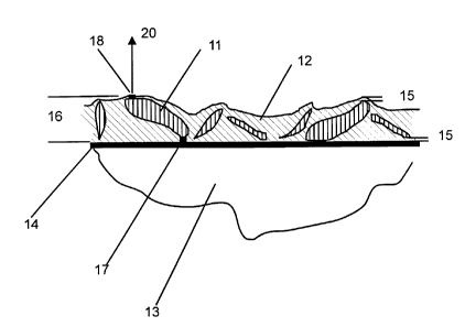
Figure 1 shows a MIMIV field emitter material;
Figures 2a and 2b show voltage-current characteristics for two
alternative cathodes;
Figures 3a and 3b show, for comparison, emission images for the
cathodes of Figures 2a and 2b respectively;
Figure 4 shows an emission image of a cathode; and
Figures Sa to Sc show respective examples of field-emitting
devices using materials as disclosed herein.
Figure 1 shows a MIMIV emitter material as described by Tuck,
Taylor and Latham (GB 2304989) with electrically conducting particles 11 in
an inorganic electrically insulating matrix 12 on an electrically conducting
substrate 13. For insulating substrates 13, an electrically conducting layer
14
is applied before coating. The conducting layer 14 may be applied by a
variety of means including, but not limited to, vacuum and plasma coating,
electro-plating, electroless plating and ink based methods.
CA 02378454 2002-O1-04
WO 01/03154 PCT/GB00/02537
-12-
Whilst embodiments of the present invention are not limited to a
particular emission mechanism, the emission process of the material shown
in Figure 1 is believed to occur as follows. Initially the insulator 12 forms
a
blocking contact between the particles 11 and the substrate. The voltage of a
particle will rise to the potential of the highest equipotential it probes -
this
has been called the antenna effect. At a certain applied voltage, this will be
high enough to create an electro-formed conducting channel 17 between the
particle and the substrate. The potential of the particle then flips rapidly
towards that of the substrate 13 or conducting layer 14, typically arranged as
a cathode track. The residual charge above the particle then produces a high
electric field which creates a second electro-formed channel 18 and an
associated metal-insulator-vacuum (MI~ hot electron emission site. After
this switch-on process, reversible field emitted currents 20 can be drawn from
the site.
The standing electric field required to switch on the electro-
formed channels is determined by the ratio of particle height 16 and the
thickness of the matrix in the region of the conducting channels 15. For a
minimum switch on field, the thickness of the matrix 12 at the conducting
channels should be significantly less than the particle height. The conducting
particles would typically be in, although not restricted to, the range
0.1 microns (micrometres) to 400 microns, preferably with a narrow size
distribution.
By a "channel", "conducting channel" or "electro-formed channel"
we mean a region of the insulator where its properties have been locally
modified, usually by some forming process involving charge injection or
heat. Such a modification facilitates the injection of electrons from the
CA 02378454 2002-O1-04
WO 01/03154 PCT/GB00/02537
-13-
conducting back contact into the insulator such that the electrons may move
through it, gaining energy, and be emitted over or through the surface
potential barrier into the vacuum. In a crystalline solid the injection may be
directly into the conduction band or, in the case of amorphous materials, at
an energy level where hopping conduction is possible.
We have now found, surprisingly, that carefully controlled
variants of amorphous silica can provide an ideal material for the insulator
component in a MIMIV structure. Unlike many candidate amorphous
materials, amorphous silica has a diffused (tail states that may or may not be
localised) but well defined band gap and can thus have its properties modified
using analogues of semiconductor engineering techniques (e.g. doping) to
provide donor levels to give the material desirable n-type properties. The
role of these donor levels is described in our co-pending application GB 2 340
299, to which the reader's attention is directed. It should be realised that,
as
with all amorphous materials, the dopant concentrations required to produce
electronic effects are much higher than for crystalline materials. In some
cases, alloying of the material may also occur due to the high concentration
of impurities introduced into the structure. As well as the addition of
dopants, the electrical properties of the silica can be modified by
controlling
the morphology of the film with defects in the lattice and grain boundaries to
provide donors and internal field concentration points. We have found that
a high quality silica film that is electrically perfect does not provide the
necessary carriers/states for conduction. Furthermore, we have found that
non-optimised or incorrectly processed formulations can all too easily lead to
silica that is too perfect.
CA 02378454 2002-O1-04
WO 01/03154 PCT/GB00/02537
-14-
Silica (SiO~ is a complicated polymorphic structure consisting of
silicon and oxygen atoms in a tetrahedral arrangement in which the
tetrahedra are joined at the corners by bridging oxygen bonds. Defect-free
silica necessarily implies a pure and perfect crystalline material with sharp
band edges that have no tail states.
Considerable effort has been expended in the semiconductor
industry to grow virtually defect-free amorphous silica films by thermally
oxidising silicon. This results in an electronic grade of silica used as the
gate
dielectric for metal-oxide-semiconductor devices. These have a low density
of defects, making them resistant to high-voltage breakdown.
On the other hand, silica deposited by plasma, sol-gel or
polymeric precursor routes is amorphous with the disorder being
compositional, structural or morphological. For example, it contains a much
higher density of point defects, such as dangling bonds, non-bridging oxygen
bonds, and hydrogen terminated bonds than thermally grown silica. This
makes the material non-stoichiometric. The electrical properties of such films
are determined by, among other factors, the deposition, impurity additions,
and subsequent annealing. Annealing could be carried out by traditional
furnaces, rapid thermal annealing or with the use of lasers.
Hence, by controlling the deposition technique and avoiding
prolonged post-annealing, it is possible to controllably create heavily
defective silica. Such materials can be described as having many electronic
states that may, or may not, be localised such that they extend into the band-
gap. This results in wide fuzzy band-edges, often referred to as band tails,
and a reduction in the overall band-gap.
CA 02378454 2002-O1-04
WO 01/03154 PCT/GB00/02537
-15-
Such heavily defective silica will have been avoided by the
traditional electronics industry trying to grow good dielectric thin films,
primarily because of its poor resistance to electrical breakdown. This
property arises from a variety of charged and neutral states providing a
conduction path through the material, for example by hopping conduction
and ionic processes.
Silica films with the correct properties may be fabricated using sol-
gel methods with the formulation of the dispersion, the coating process and
the layer's subsequent heat treatment being critical to final emitter
performance.
Exemplary processes for forming such sol-gels are as follows.
Example 1
Tetraethyl orthosilicate (10 ml), and MOS grade propan-2-of (47
ml) were mixed and cooled to 5-10°C with stirring at 1000 r.p.m. To
this
stirring mixture was than added a solution of concentrated nitric acid (0.10
g)
in deionised water (2.5 g). After 2 hours, the mixture was transferred to a
sealed container, and stored at 4°C in a refrigerator until required.
Example 2
Tetraethyl orthosilicate (10 ml), acetone (13 ml), and MOS grade
propan-2-of (34 ml) were mixed and cooled to 5-10°C with stirring at
1000 r.p.m. To this stirring mixture was then added a solution of
concentrated hydrochloric acid (0.25 g) in deionised water (2.5 g). After 2
hours, the mixture was transferred to a sealed container, and stored at
4°C in
a refrigerator until required.
CA 02378454 2002-O1-04
WO 01/03154 PCT/GB00/02537
-16-
Example 3
Tetraethyl orthosilicate (10 ml), acetone (13 ml), and MOS grade
propan-2-of (34 ml) were mixed and cooled to 5-10°C with stirring at
1000
r.p.m. To this stirring mixture was then added a solution of concentrated
nitric acid (0.10 g) in deionised water (2.5 g). After 2 hours, the mixture
was
transferred to a sealed container, and stored at 4°C in a refrigerator
until
required.
The band gap of silica may be advantageously modified by the
addition of, for example, tin oxide. Sn02 is homologous with Si02. The
band gap of silica is "9eV whilst that for Sn02 is " 3.6eV. Mixtures of the
two materials have band gaps intermediate those of the two materials.
Furthermore, Sn02 is, as the result of its tendency to be oxygen deficient, an
n-type material. Appropriate mixtures of SiOz and SnOz will thus
advantageously have both a narrower band gap than silica alone and have n-
type properties. Indium tin oxide or antimony tin oxide may also be used as
an additive.
A further means by which the electronic properties of the silica
may be modified is the addition of metallic cationic species into the
amorphous silica network. We have found that a mixture of iron and
manganese salts (e.g. nitrates) added to the sol-gel reduces the operating
field
of the emitter. Other metal salts and organometallic compounds may be
added to produce similar effects.
An exemplary process for forming such metal doped sol-gels is as
follows.
CA 02378454 2002-O1-04
WO 01/03154 PCT/GB00/02537
_17_
Example 4
Tetraethylorthosilicate (10.0 ml), acetone (13 ml), and MOS grade
propan-2-of (34 ml) were mixed and cooled to 5-10°C. To this stirring
mixture (1000 r.p.m.) was then added a solution of concentrated nitric acid
(0.1 g), Fe(N03)3.9H20 (0.125 g) and Mn(N03)2.6H20 (0.125 g) in
deionised water (2.5 ml). After 2 hours, the mixture was transferred to a
sealed container and stored in a refrigerator at 4°C.
The use of sol-gel precursors for silica is ideal for formulating
emitter inks for the formation of layers by spin coating. However, their one
disadvantage is that, once dried, they are not reverse soluble in the solvent.
This makes them unsuitable for many printing processes, such as inkjet and
silk screen, where the jets and narrow openings in the screen will become
blocked with solidified material.
Arkles (US Patent 5,853,808) describes the use of silsequioxane
polymers as precursors for the preparation of high quality silica-rich films
for
use in electronic devices and therefore, as discussed herein, desirably as
perfect as possible. We have found these materials to be useful alternatives
to
sol-gel dispersions in the formulation of emitter inks. These materials are
reverse soluble in a number of solvents, for example methoxypropanol.
One polymer, (3-chloroethylsilsesquioxane, has been found to be particularly
useful. In the case of this work processing is controlled. We have found that
by carefully controlling the processing we can, unlike Arkles, produce
deliberately defect-rich films.
Another useful property of formulations based upon these
silsequioxane polymers is that they may be converted to silica using
CA 02378454 2002-O1-04
WO 01/03154 PCT/GB00/02537
-18-
ultraviolet radiation as well as heat. This enables one not only to cure the
films via blanket (broad area) irradiation but also to use optical
lithographic
techniques, including the use of cursive exposure by laser, to form patterned
emitters.
Other polymer precursors can also be used.
Moving on now to the choice of particle, we have found that,
surprisingly, one material, graphite, is far superior to all others.
By graphite particles we mean ones in which the so-called prism
planes are exposed either at fractured edges or steps and terraces on the
basal
plane. ~XTithin this definition we include carbon nanotubes, preferably but
not exclusively un-capped, single and multi-wall.
This preference for one particle material is surprising since, at first
sight, the particle's role is primarily that of an electric field enhancing
element. However, the surface of the particle forms the back contact of the
MIV channel in the MIMIV emission mechanism. It is known in the art, and
addressed in our co-pending application GB 2 340 299 that this surface plays
an important role in the injection of electrons into an insulator layer.
Furthermore, electrostatic modelling has shown us that the lower metal-
insulator-metal (MINI) channel has a higher field across it prior to forming
than the MIV channel and consequently the composition of its back contact
(Figure 1 13/14) is far less critical - this is confirmed by our experiments.
The preference for graphite is very specific, as other conducting
forms of carbon do not show the same superior performance. For example,
carbon black particles which are complex in shape (e.g. aciniform), and thus
likely to provide good electric field enhancement, do not result in good
CA 02378454 2002-O1-04
WO 01/03154 PCT/GB00/02537
-19-
emitters. This is despite the fact that the exposed surface is
crystallographically very similar to the basal plane of graphite.
We speculate that the open prism planes and the steps and terraces
upon the basal plane provides an atomically rough surface which enables the
oxygen atoms in the silica to sit "in" the graphite surface, reducing the
negative dipole that would otherwise result. This arrangement facilitates the
injection of electrons from the graphite into the silica. Similar effects have
been observed on thermionic dispenser cathodes (see Norman, Tuck et al
Physical Review Letters tlol. 58, No. S, 2"d Feb. 1987 page 519). Further
evidence
of the special nature of graphite is that other flake-like materials, such as
nickel and silver-plated nickel, are, surprisingly, significantly inferior.
Suitable graphite particles may be obtained from:
Timcal SA
Grafite a Tecnologie
CH-6743-Bodio
Switzerland
Their grades KS4, KS6 and KS15 (where the number indicates the
nominal particle size in micrometres) are particularly useful. Clearly, other
sources may be found by those skilled in the art.
Finely divided graphite may also be coated onto particles that have
other desirable properties, for example a higher resistivity, to form
composite
structures. One suitable host particle is boron carbide. One method of
adding such a coating is to add colloidal graphite to the emitter ink.
An exemplary processes for forming an emitter ink using graphite
particles is as follows.
CA 02378454 2002-O1-04
WO 01/03154 PCT/GB00/02537
-20-
Example 5
Timrex KS6 graphite (0.150 g) and a sol-gel dispersion according to
Example 1 (9.850 g) previously filtered through a 0.2 micron filter were
mixed, and ultrasonically agitated for 10 minutes using a high power
ultrasonic probe. The sample was allowed to cool to room temperature and
ultrasonically agitated for a further 10 minutes. This yielded the required
ink
as a black suspension. The mixture was transferred to a sealed container and
stored in a refrigerator at 4°C.
Example 6
Timrex KS6 powder (0.049 g) and Gelest Seramic Si (9.945 g)
prefiltered through a 0.2 micron filter were mixed and agitated for 10
minutes using a high power ultrasonic probe. The mixture was transferred to
a sealed container and stored in a refrigerator at 4°C.
Note: Gelest Seramic Si is a proprietary solution of (3-chloroethyl-
silsesquioxane in methoxypropanol.
Dispersants or surfactants can be used in embodiments of the
invention to facilitate the dispersions of particles in the liquid media.
Exemplary processes for forming field emitting cathodes using the
inks described in Examples 5 and 6 are as follows.
CA 02378454 2002-O1-04
WO 01/03154 PCT/GB00/02537
-21 -
Example 7
A borosilicate glass substrate is coated with gold, either by sputter
coating (nichrome under-layer for adhesion) or by the use of liquid bright
gold.
By liquid bright gold we mean metallic layers produced using a
paint that contains organometallic compounds - the so-called resinate or
bright golds, palladiums and platinums. The metallic layer is formed by
applying a paint and then firing the object in air at temperatures between
480°C and 920°C, at which point the organometallic compound
decomposes
to yield pure metal films 0.1 to 0.2 ~.m thick. Traces of metals such as
rhodium and chromium are added to control morphology and assist in
adhesion. Currently, most of these known products and development
activity concentrate on the decorative properties of the films. However, the
technology is well established. Although little (or not) used, or known of, in
the field emission art today, such techniques have been used in the past by
the electron tube industry. For example Fred Rosebury's classic text
"Handbook of Electron Tube and hacuum Techniques " originally published in
1964 Reprinted by American Institute of Physics - ISBN 1-56396-121-0~ gives a
recipe for liquid bright platinum. More recently, Koroda (US Patent
4,098,939) describes their use for the electrodes in a vacuum fluorescent
display.
The chosen ink (e.g. from the above examples) was removed from
the refrigerator and allowed to warm up to room temperature. The substrate
was the placed on the vacuum chuck of a spin coating machine. The
substrate was spun up to coating speed (typically 3000 r.p.m to 8000 r.p.m)
and flooded with MOS grade propan-2-of as a cleaning process.
CA 02378454 2002-O1-04
WO 01/03154 PCT/GB00/02537
-22-
The ink was agitated just prior to application. The substrate was
then run up to coating speed (typically 3000 r.p.m to 8000 r.p.m) and the ink
applied with a pipette near to the centre of rotation of the substrate at the
rate of 0.2 ml cm 2 to 0.4 ml cm 2. Following application, the substrate
continued to rotate at full speed for a further 10 seconds.
After the substrates were spin coated they were transferred to
hotplates under the following conditions: a) 10 minutes at 50°C -
measured
surface temperature of hotplate; b) 10 minutes at 120°C - measured
surface
temperature of hotplate. The substrates were then transferred to an oven (air
atmosphere) according to the following profile: ambient to 450°C at
10°C/min; isotherm at 450°C for 120 minutes; followed by cooling
naturally
to room temperature. The rate and method (i.e. hotplate) of the early
heating steps are critical to film integrity and emitter performance.
Following heat treatment, the emitters were ultrasonically cleaned
for between 10 and 60 seconds in MOS grade propan-2-ol.
The emitters were then dried using an air duster, and placed on a
hotplate for 2 minutes at 50°C in order to remove any remaining
solvent.
Example 8
A borosilicate glass substrate is coated with a reactively sputtered
layer- " 1 micrometre thick of chromium oxide on a metallic chromium layer
" 0.5 micrometer thick. The stoichiometry of this oxide may be adjusted to
control the resistivity of the oxide film to provide resistive ballasting to
control emitter site currents.
CA 02378454 2002-O1-04
WO 01/03154 PCT/GB00/02537
-23-
The chosen ink (e.g. from the above examples) was removed from
the refrigerator and allowed to warm up to room temperature. The substrate
was then placed on the vacuum chuck of a spin coating machine. The
substrate was spun up to coating speed (typically 3000 r.p.m to 8000 r.p.m)
and flooded with MOS grade propan-2-of as a cleaning process.
The ink was agitated just prior to application. The substrate was
then run up to coating speed (typically 3000 r.p.m to 8000 r.p.m) and the ink
applied with a pipette near to the centre of rotation of the substrate at the
rate of 0.2 ml cm Z to 0.4 ml cm Z. Following application the substrate
continued to rotate at full speed for a further 10 seconds.
After the substrates were spin coated they were transferred to
hotplates under the following conditions: a) 10 minutes at 50°C -
measured
surface temperature of hotplate; b) 10 minutes at 120°C - measured
surface
temperature of hotplate. The substrates were then transferred to an oven (air
atmosphere) according to the following profile: ambient to 450°C at
10°C/min; isotherm at 450°C for 120 minutes; followed by cooling
naturally
to room temperature. The rate and method (i.e. hotplate) of the early
heating steps are critical to film integrity and emitter performance.
Following heat treatment, the emitters were ultrasonically cleaned
for between 10 and 60 seconds in MOS grade propan-2-ol.
The emitters were then dried using an air duster, and placed on a
hotplate for 2 minutes at 50°C in order to remove any remaining
solvent.
We have found that, provided care is taken, emitters prepared in
accordance with the above methods can be patterned using a lift-off process.
CA 02378454 2002-O1-04
WO 01/03154 PCT/GB00/02537
-24-
An exemplary process for patterning field emitting cathodes using
the inks as in Example 5 is as follows:
Example 9
1. Substrates with conducting coatings were cleaned in an
ultrasonic bath in MOS grade acetone for 1 minute, holding
the substrates with plastic tweezers, and moving the beaker
containing the acetone around the bath. Both sides of the
substrates were then rinsed with a jet of MOS grade propan-2-
ol and dried with an airduster. The substrates were then dried
on a hotplate at 50°C for a few minutes.
2. The substrates were then cleaned with an oxygen plasma in an
Oxford Plasma Technology RIE80 at 100V~Iatts power,
200mtorr pressure, 35sccm oxygen for one minute.
3. JSR resist type IX500 was then spun onto the substrate - 2m1 of
resist was pipetted onto the slide which was then spun at
1000rpm for ~ 5 seconds and then 3000rpm for ~50seconds.
4. The resist was then baked for 2 minutes on a hotplate at 100°C
and the substrate allowed to cool.
5. Exposure of the resist was carried out with a chrome/glass
mask on a SET mask aligner. The exposure time was 15
seconds (30m~X1 cm 2 s 1).
6. The substrates were then baked again on a hotplate at 100°C
for 2 minutes.
CA 02378454 2002-O1-04
WO 01/03154 PCT/GB00/02537
-25-
7. The pattern was then developed in JSR developer type
TMA238WA for 20 seconds. The slides were rinsed with
deionised water and then blow dried with nitrogen.
8. A hard bake was then carried out in an oven at 140°C for
10 minutes.
9. A descum process was then carried out on the substrates in an
Oxford Plasma Technology RIE80 at 50 Watts power,
200mtorr pressure, 35sccm oxygen for 0.7 minute. By
"descum" is meant a cleaning step to promote adhesion, such as
but not limited to an oxygen plasma etch, that removes any
traces of photoresist chemicals from the areas where the
emitter patches are to be coated.
10. The ink as described in Example 5 was removed from the
refrigerator and allowed to warm up to room temperature.
The substrate was then placed on the vacuum chuck of a spin
coating machine.
11. The ink was agitated just prior to application. The substrate
was then run up to coating speed (typically 3000 r.p.m to 8000
r.p.m) and the ink applied with a pipette near to the centre of
rotation of the substrate at the rate of 0.2 ml cm 2 to
0.4 ml cm Z . Following application the substrate continued to
rotate at full speed for a further 10 seconds.
12. After the substrates were spin coated they were transferred to
hotplates under the following conditions: a) 10 minutes at
CA 02378454 2002-O1-04
WO 01/03154 PCT/GB00/02537
-26-
50°C - measured surface temperature of hotplate; b) 10 minutes
at 120°C - measured surface temperature of hotplate.
13. cFor the lift-off process the substrate was held with plastic
tweezers in MOS grade acetone in the ultrasonic bath for 10 -
20 seconds whilst moving it around.
14. The substrate was then rinsed on both sides with MOS grade
acetone and then with MOS grade propan-2-ol. It was dried
with an airduster and put on the hotplate at 50°C to ensure it
was completely dried.
15. Inspection micrographs were then recorded on a
metallographic microscope.
16. The substrates were then transferred to an oven (air
atmosphere) according to the following profile: ambient to
450°C at 10°C/min; isotherm at 450°C for 120 minutes;
followed by cooling naturally to room temperature.
17. Following heat treatment, the emitters were ultrasonically
cleaned for between 10 and 60 seconds in MOS grade propan-2-
o1.
Figure 4 shows an emission image of a cathode patterned using the
above technique - the letters are 6 mm high. For clarity of view and to
facilitate reproduction, the view of Figure 4 is shown in reverse video - that
is, original light spots against a dark background are shown in Figure 4 as
dark spots against a light background.
CA 02378454 2002-O1-04
WO 01/03154 PCT/GB00/02537
_27_
All of the processes described herein are merely examples that can
be changed or adapted by someone skilled in the art without deviating from
the teachings of this invention. Although examples are given above of a
MIMIV emission mechanism, other embodiments of the invention may
operate by other emission mechanisms, including MIV mechanisms.
In all of the above examples, the resultant silica is amorphous silica
which is doped and/or is heavily defective. An important feature of the
processing of the silica precursor, whether by heating, ultra-violet exposure
or other means, is that processing is not continued until the silica precursor
has been processed as far as it can, into a highly dense state. On the
contrary,
processing is carefully controlled to ensure that the resultant amorphous
silica is not processed into its densest possible state, but is heavily
defective.
To illustrate the differences between graphite and non-ideal
particles, Figure 2a shows voltage-current characteristics for a cathode made
using the ink described in Example 5, and Figure 2b shows one in which, all
other factors being equal, the graphite has been replaced with angular
titanium diboride particles of similar resitivity. Both dispersions were
coated
and processed according to Example 7. To obtain the data, the 26 mm square
samples were mounted 0.25 mm away from a tin oxide coated glass anode.
The voltage applied to the diode was varied under computer control, with
images of the electron bombardment induced fluorescence on the tin oxide
coated anode being viewed by a CCD camera. Figure 2a shows a plot for an
emitter containing the KS6 graphite, whilst Figure 2b shows data for the
titanium diboride sample. Note the need for a higher field and the
dramatically reduced current (different scale) in Figure 2b.
CA 02378454 2002-O1-04
WO 01/03154 PCT/GB00/02537
-28-
Figure 3 compares emission images captured by the CCD camera
for the cathodes containing graphite (Figure 3a) and titanium diboride
(Figure 3b). Note that many hundreds of emitters sites are visible in Figure
3a, whilst there are only two in Figure 3b. The field of view is 26 mm x 26
mm. For clarity of view and to facilitate reproduction, the views of Figures
3a and 3b are shown in reverse video - that is, original light spots against a
dark background are shown in the figures as dark spots against a light
background.
Improved emitter materials embodying the invention may be used
also in MIV devices (see, for example, our patent application GB 2 332 089),
and where conductive "particles" are provided by particle-like projections or
tips fabricated on a substrate and coated with an insulating layer. In
embodiments of the invention, the conducting substrate, or conducting layer
on the substrate, may be of graphite.
The field electron emission current available from improved
emitter materials such as are disclosed above may be used in a wide range of
devices including (amongst others): field electron emission display panels;
lamps; high power pulse devices such as electron MASERS and gyrotrons;
crossed-field microwave tubes such as CFAs; linear beam tubes such as
klystrons; flash x-ray tubes; triggered spark gaps and related devices; broad
area x-ray sources for sterilisation; vacuum gauges; ion thrusters for space
vehicles and particle accelerators.
Examples of some of these devices are illustrated in Figures Sa,
5b and 5c.
CA 02378454 2002-O1-04
WO 01/03154 PCT/GB00/02537
-29-
Figure 5a shows an addressable gated cathode as might be used in
a field emission display. The structure is formed of an insulating substrate
500, cathode tracks 501, emitter layer 502, focus grid layer 503 electrically
connected to the cathode tracks, gate insulator 504, and gate tracks 505.
The gate tracks and gate insulators are perforated with emitter cells 506. A
negative bias on a selected cathode track and an associated positive bias on a
gate track causes electrons 507 to be emitted towards an anode (not shown).
The reader is directed to our co-pending application GB 2 330
687 (97 22258.2) for further details of constructing Field Effect Devices.
The electrode tracks in each layer may be merged to form a
controllable but non-addressable electron source that would find
application in numerous devices.
Figure 5b shows how the addressable structure 510 described
above may joined with a glass fritt seal 513 to a transparent anode plate 511
having upon it a phosphor screen 512. The space 514 between the plates is
evacuated, to form a display.
Although a monochrome display has been described, for ease of
illustration and explanation, it will be readily understood by those skilled
in the art that a corresponding arrangement with a three-part pixel may be
used to produce a colour display.
Figure 5c shows a flat lamp using one of the above-described
materials. Such a lamp may be used to provide backlighting for liquid
crystal displays, although this does not preclude other uses, such as room
lighting.
CA 02378454 2002-O1-04
WO 01/03154 PCT/GB00/02537
-30-
The lamp comprises a cathode plate 520 upon which is deposited
a conducting layer 521 and an emitting layer 522. Ballast layers as
mentioned above (and as described in our other patent applications
mentioned herein) may be used to improve the uniformity of emission. A
transparent anode plate 523 has upon it a conducting layer 524 and a
phosphor layer 525. A ring of glass fritt 526 seals and spaces the two plates.
The interspace 527 is evacuated.
The operation and construction of such devices, which are only
examples of many applications of embodiments of this invention, will
readily be apparent to those skilled in the art. An important feature of
preferred embodiments of the invention is the ability to print an emitting
pattern, thus enabling complex multi-emitter patterns, such as those
required for displays, to be created at modest cost. Furthermore, the ability
to print enables low-cost substrate materials, such as glass to be used;
whereas micro-engineered structures are typically built on high-cost single
crystal substrates. In the context of this specification, printing means a
process that places or forms an emitting material in a defined pattern.
Examples of suitable processes are (amongst others): screen printing,
Xerography, photolithography, electrostatic deposition, spraying, ink jet
printing and offset lithography.
Devices that embody the invention may be made in all sizes,
large and small. This applies especially to displays, which may range from a
single pixel device to a multi-pixel device, from miniature to macro-size
displays.
In this specification, the verb "comprise" has its normal
dictionary meaning, to denote non-exclusive inclusion. That is, use of the
CA 02378454 2002-O1-04
WO 01/03154 PCT/GB00/02537
-31 -
word "comprise" (or any of its derivatives) to include one feature or more,
does not exclude the possibility of also including further features.
The reader's attention is directed to all papers and documents
which are filed concurrently with or previous to this specification in
connection with this application and which are open to public inspection
with this specification, and the contents of all such papers and documents
are incorporated herein by reference.
All of the features disclosed in this specification (including any
accompanying claims, abstract and drawings), and/or all of the steps of any
method or process so disclosed, may be combined in any combination,
except combinations where at least some of such features and/or steps are
mutually exclusive.
Each feature disclosed in this specification (including any
accompanying claims, abstract and drawings), may be replaced by
alternative features serving the same, equivalent or similar purpose, unless
expressly stated otherwise. Thus, unless expressly stated otherwise, each
feature disclosed is one example only of a generic series of equivalent or
similar features.
The invention is not restricted to the details of the foregoing
embodiment(s). The invention extends to any novel one, or any novel
combination, of the features disclosed in this specification (including any
accompanying claims, abstract and drawings), or to any novel one, or any
novel combination, of the steps of any method or process so disclosed.