Note: Descriptions are shown in the official language in which they were submitted.
CA 02378457 2002-01-04
WO 01/05008 PCT/GBOO/02550
1
Control of Polarisation of Vertical Cavity Surface Emitting Lasers
The present invention relates to the control of the polarisation of light
emitted by Vertical Cavity Surface Emitting Lasers or VCSELs.
Recently there has been increased interest in VCSELs because they
have several potential advantages over conventional edge emitting
semiconductor lasers, such as planar construction, the emission of light
perpendicular to the surface of the semiconductor substrate and the
possibility of fabrication in an array. Edge emitting lasers have the
advantage of emitting polarised light, however they emit an elliptical
beam of polarised light which requires the use of a lens to couple the
elliptical beam to a circular optical fibre. By comparison VCSELs which
in their simplest form have a semiconductor structure which is axially
symmetric about the vertical axis of the VCSEL will emit a circular beam
of light which is unpolarised. A circular beam can be directly coupled
into a circular optical fibre without the use of a lens, or at least using a
simplified lens structure.
For many proposed applications for VCSELs, such as sources for
spatial light modulators, it is desirable, and in some cases necessary to
have single mode operation of VCSELs with a well defined polarisation
of light, that is, the direction of the electric field vector of the light
emitted
by the VCSEL has to be well defined and must not change with current
or temperature. To achieve this a differential gain has to be introduced
for two orthogonal polarisations of light generated in the gain region of
the VCSEL.
This problem has been tackled by altering the semiconductor structure
of the VCSEL from a simple axially symmetrical structure to a more
complex structure in which the VCSEL comprises a waveguide which
preferentially supports one orthogonal polarisation. This approach is
CA 02378457 2002-01-04
WO 01/05008 PCT/GBOO/02550
2
used in JP10223973 and EP772269 and results in a more complicated
semiconductor structure which can reduce the circular symmetry of the
beam of light generated by the VCSEL. EP772269 also discloses the
use of a non-symmetrical emission port on a VCSEL to promote one
orthogonal polarisation, but again this will reduce the circular symmetry
of the beam of light generated by the VCSEL. US 5,727,014 also
discloses the use of a non-symmetrical emission port on a VCSEL,
which port is surrounded by an electrode of the VCSEL.
In US5412680 the active layer of the VCSEL comprises at least one
strained semiconductor layer having a preferential direction of electrical
conductivity along a direction parallel to the mirrors of the VCSEL so
that the VCSEL emits light having a polarisation substantially parallel to
this preferential direction. However, this straining of the semiconductor
material adds complexity to the structure of the VCSEL. Furthermore,
the strained layer must be relatively thin and such thin layers are difficult
to reproduce accurately in bulk manufacture, resulting in VCSELs
whose properties are not very reproducible. Alternatively, the active
layer of the VCSEL can be elongated so that the polarisation of the
radiation emitted by the VCSEL is parallel to the longitudinal axis of the
active layer. In GB 2,311,166 a multi-layer polymeric Bragg reflector is
stretched to orient polymer molecules to define a direction of
polarisation.
In JP09181391 the VCSELs are grown with their axes of symmetry
inclined to the vertical in order to promote the generation of one
orthogonal polarisation. However, the inclined structure of the VCSELs
complicates the fabrication process used to form the individual VCSELs
because undercutting will be required.
In JP09283859 and JP09283860 ring electrodes on one end surface of
a VCSEL are used to switch between two orthogonal polarisations.
CA 02378457 2002-01-04
WO 01/05008 PCT/GBOO/02550
3
The present invention aims to provide a VCSEL which overcomes at
least some of the problems discussed above. In particular the present
invention aims to provide a VCSEL which emits a circular beam of
polarised light and yet which maintains a simple structure to ease
fabrication.
According to a first aspect of the present invention there is provided a
vertical cavity surface emitting laser (VCSEL) comprising a one
dimensional grating structure located at an end of the VCSEL for
selectively promoting the gain of a first polarisation of light within the
VCSEL as compared to the gain of a second orthogonal polarisation of
light within the VCSEL. The VCSEL will therefore tend to lase at the
first polarisation.
Thus, a polarisation controlled VCSEL is provided using a standard
VCSEL structure with only one additional structure added to one of its
ends. Thus, fabrication of a VCSEL according to the present invention
can be simplified relative to the polarisation controlled VCSELs already
known in the prior art. Furthermore, the arrangement according to the
present invention will not reduce the symmetry of the circular beam
emitted by the VCSEL. The present invention also enables arrays of
polarisation controlled VCSELs of the same polarisation to be fabricated
by fabricating the same one dimensional grating structure over the
entire array of VCSELs in a single processing step.
Preferably, the one dimensional grating structure is located at an end of
the VCSEL as this generates a structure that is simple and relatively
easy to fabricate.
In a preferred embodiment the one dimensional grating structure is
located at the top end of the VCSEL. This is preferred particularly if the
grating structure is made of metal because it is presently not possible to
CA 02378457 2002-01-04
WO 01/05008 PCT/GB00/02550
4
grow the layers of semiconductor material that make up a VCSEL over a
layer of metal.
The polarisation controlled VCSELs according to present invention can
be arranged to emit light from their top end surface or from their bottom
end surface as required.
In one embodiment the one dimensional grating structure can reflect
both the first and second orthogonal polarisations of light back into the
cavity of the VCSEL. The gain of the first polarisation can then be
selectively promoted by arranging light of the first polarisation reflected
by the grating structure to interfere constructively with other light of the
first polarisation reflected back into the VCSEL cavity (eg. due to the
arrangement of the layers of a Bragg mirror, and/or by arranging for light
of the second orthogonal polarisation reflected by the grating structure
to interfere destructively with other light of the second polarisation
reflected back into the VCSEL cavity.
In an alternative embodiment the one dimensional grating structure can
be arranged to preferentially reflect the first polarisation of light back
into
the cavity of the VCSEL. The VCSEL then will tend to lase at the first
polarisation which is preferentially reflected back into the cavity of the
VCSEL, provided it is reflected back in such a way that it is in phase
with the light of the first polarisation which is also reflected back into the
laser cavity, for example by the layers of a Bragg stack mirror. This is
because there will be a higher electric field intensity within the cavity, ie.
a higher gain, at this first polarisation.
The one dimensional grating structure can be arranged to preferentially
absorb the second orthogonal polarisation of light, so that the VCSEL
lases with the first preferentially reflected polarisation of light.
CA 02378457 2002-01-04
WO 01/05008 PCT/GBOO/02550
The one dimensional grating structure can be arranged to preferentially
transmit the first orthogonal polarisation of light with the advantage that
if the VCSEL is arranged to lase with this first polarisation, light can be
coupled out of the VCSEL via the one dimensional grating structure.
5
In embodiments of the present invention in which the VCSEL also
includes a Bragg stack adjacent to the one dimensional grating structure
for reflecting light back into the cavity of the VCSEL, it is preferred that
the structure of the VCSEL is arranged such that the grating structure
and the Bragg stack reflect the first polarisation of light back into the
VCSEL cavity substantially in phase to promote constructive
interference between the reflected light of the first polarisation.
Alternatively, or in addition to this, the structure of the VCSEL can be
arranged such that the grating structure and the Bragg stack reflect the
second polarisation of light back into the VCSEL cavity substantially out
of phase to promote destructive interference between the reflected light
of the second polarisation.
The VCSEL according to the present invention preferably comprises an
upper Bragg mirror, a gain region, and a lower Bragg mirror, and the
grating structure is located in an end layer of the VCSEL and the end
layer and/or optionally an adjacent layer of the Bragg mirror has a
thickness such that the reflected light, reflected by the one dimensional
grating structure, of the first polarisation constructively interferes with
light of that first polarisation which is reflected by said one of the Bragg
mirrors (i.e it is in phase). As described above this ensures that the
VCSEL lases with the first polarisation, eg. the polarisation that is
preferentially reflected by the one dimensional grating structure.
Alternatively or additionally, said end layer or said adjacent layer of the
Bragg mirror may have a thickness such that the reflected light of the
second polarisation, reflected by the one dimensional grating structure,
destructively interferes with light of that second polarisation which is
CA 02378457 2002-01-04
WO 01/05008 PCT/GBOO/02550
6
reflected by the said one of the Bragg mirrors (i.e. it is out of phase).
This ensures that the electric field intensity in the cavity is smaller for
the second polarisation due to the destructive interference than for the
first polarisation. This can be the case even if the second polarisation of
light is preferentially reflected back into the VCSEL cavity because, for
example, the first polarisaton is preferentially transmitted by the grating
structure in order to couple light of the first polarisation out of the
VCSEL.
Where the layers of the Bragg mirror are planar and the one
dimensional diffraction grating structure is not located at an end of the
VCSEL, any layers of a Bragg mirror located above the grating structure
(in the direction of VCSEL growth) would have to be planarised as part
of the fabrication process. An alternative would be to use a Bragg
mirror having corrugated layers and by arranging the corrugations in the
Bragg layers to have dimensions corresponding to the dimensions of the
corrugations of the grating structure.
In a first preferred embodiment the one dimensional grating structure
comprises a corrugated metal mirror arranged such that light of a
polarisation with the electric vector perpendicular to the grating grooves
incident on the corrugated metal mirror generates surface plasmon
polaritons. This polarisation is preferentially absorbed by the corrugated
metal mirror and the orthogonal polarisation is preferentially reflected by
the corrugated metal mirror back into the VCSEL cavity. Preferably the
pitch of the corrugations of the corrugated metal mirror XG is
determined by the following equation:
2-nm/21c = Kspp
where Kspp is the wave vector of the surface plasmon polaritons, and m
is an integer. Ideally one would choose m=1 so that there are no
CA 02378457 2002-01-04
WO 01/05008 PCT/GBOO/02550
7
diffracted orders (i.e. the grating is zero order). The corrugated metal
mirror may be made of any metal, preferably one which also acts as a
good electrical contact (e.g. gold).
According to this first preferred embodiment the surface plasmon
polaritons may be generated at the interface between the corrugated
metal mirror and an upper Bragg mirror of the VCSEL. In this
configuration the VCSEL will be bottom emitting. However, a top
emitting VCSEL can be produced if the surface plasmon polaritons are
generated at the interface between the corrugated metal mirror and air,
which is possible if the one dimensional metal grating is optically thin
(about one wavelength in thickness). This also increases kc, making the
corrugated metal mirror simpler to fabricate.
A second preferred embodiment comprises a VCSEL having a one
dimensional grating structure comprising a first order one dimensional
diffraction grating which is formed as a layer of the VCSEL, preferably
as an end layer of the VCSEL, and said layer is configured to act as a
waveguide in a direction perpendicular to the axis of the VCSEL and the
grating has a pitch chosen so that part of the light from the VCSEL
cavity incident normal to the grating grooves is reflected directly back
into the VCSEL cavity and part of light from the VCSEL cavity incident
normal to the grating grooves is indirectly reflected back into the VCSEL
by being diffracted into the waveguide and subsequently diffracted back
out of the waveguide and into the VCSEL cavity, in such a way that for
the second polarisation of light the indirectly reflected light interferes
destructively with the directly reflected light. The first order one
dimensional diffraction grating may be made of either a dielectric
material or a metal. The pitch of the grating is chosen so that part of the
light from the VCSEL cavity incident normal to the grating grooves is
diffracted at the interface between the top of the grating and the medium
above it (eg. air) into the waveguide formed by the grating layer,
10-02-2001 PCT/GB00/02550 DESCPAMD ,
CA 02378457 2002-01-04
8
producing a diffraction beam which travels at some angle 0
to the grating normal. This diffracted beam is reflected
further along the waveguide when it is incident on the
interface between the grating and the top of an adjacent
Bragg mirror and then diffracts from the interface at the
top of the grating once more to produce a beam travelling
normal to the grating grooves back into the VCSEL cavity.
The phase of this indirectly reflected beam depends upon
the grating pitch, the thickness of the layer in which the
grating is formed and crucially on the polarisation of the
light. Thus a grating pitch and layer thickness can be
chosen such that for the second polarisation the overall
reflectivity of the Bragg stack-grating combination is very
low (due to destructive interference between the directly
and indirectly reflected light) whilst for the first
orthogonal polarisation the reflectivity is very high. In
this case the VCSEL will lase with the first polarisation
as this has the highest gain.
According to a second aspect of the present invention there
is provided a method of controlling the polarisation of
light emitted by a vertical cavity surface emitting laser
(VCSEL) comprising the steps of using a one dimensional
grating structure, preferably located at an end of the
VCSEL, to selectively promote the gain of a first
polarisation of light within the VCSEL as compared to the
gain of a second orthogonal polarisation of light within
the VCSEL. The method according to the second aspect of
the present invention has the same advantages and preferred
Printed:06-04-2001 AMENDED SHEET 1
-02-200a_ PI..OTJGBDf3l()25a4 D~SCRAMD:
CA 02378457 2002-01-04
8a
5 features as the VCSEL according to the first embodiment of
the present invention.
According to a first preferred embodiment of the second
aspect of the present invention there is provided a method
10 of controlling the polarisation of light emitted by a
vertical cavity surface emitting laser (VCSEL) comprising
the steps of using a one dimensional grating structure to
preferentially promote the gain of a first polarisation of
light as compared to the gain of a second polarisation of
light within the VCSEL wherein the one dimensional grating
structure comprises a first order one dimensional
diffraction grating which is formed as a layer of the VCSEL
and said layer is configured to act as a waveguide in a
direction perpendicular to the axis of the VCSEL and the
grating has a pitch chosen so that part of the light from
the VCSEL cavity incident normal to the grating grooves is
reflected directly back into the VCSEL cavity and part of
the light from the VCSEL cavity incident normal to the
grating grooves is indirectly reflected back into the VCSEL
by being diffracted into the waveguide and the subsequently
diffracted back out of the waveguide and into the VCSEL
cavity, in such a way that for the second polarisation of
light the indirectly reflected light interferes
destructively with the directly reflected light.
According to a second preferred embodiment of the second
aspect of the present invention the one dimensional grating
structure comprises a corrugated metal mirror arranged such
that light of the second polarisation incident on the
Pririted:06-04-20011 AMENDED SHEET ;2
CA 02378457 2005-08-10
29756-215
8b
mirror excites surface plasmon polaritons. Preferably, the
pitch of the one dimensional corrugated metal mirror, XG, is
determined by the following equation
27L/XG = KSPp
where Kspp is the wave vector of the surface plasmon
polaritons.
The method may comprise the step of generating the
surface plasmon polaritons at the interface between the one
dimensional corrugated metal mirror and an upper Bragg
mirror of the VCSEL. Alternatively it may comprise the step
of generating the surface plasmon polaritons at the
interface between the one dimensional corrugated metal
mirror and air.
According to an aspect of the present invention,
there is provided a vertical cavity surface emitting laser
(VCSEL), said VCSEL comprising: a cavity; and a one
dimensional grating layer, wherein the layer is a first
order one dimensional diffraction grating, said layer
comprising a waveguide extending in a direction
perpendicular to an axis of the VCSEL, said grating having a
pitch such that a portion of the light from the cavity
incident normal to the grating grooves is directly reflected
back into the cavity and a portion of the light from the
cavity incident normal to the grating grooves is indirectly
reflected back into the cavity by being diffracted into the
waveguide and subsequently diffracted back out of the
waveguide and into the cavity, wherein light having a first
polarisation is selectively promoted within the cavity as
compared to light having a second orthogonal polarisation by
the one dimensional grating layer, said grating layer
arranged such that for the second polarisation of light the
CA 02378457 2005-08-10
29756-215
8c
indirectly reflected light interferes destructively with the
directly reflected light.
According to another aspect of the present
invention, there is provided a method of controlling the
polarisation of light emitted by a vertical cavity surface
emitting laser (VCSEL) comprising the steps of: using a one
dimensional grating layer for preferentially promoting gain
of a first polarisation of light as compared to gain of a
second polarisation of light within the VCSEL, said layer is
a first order one dimensional diffraction grating which is
formed as a layer of the VCSEL; configuring said layer to
act as a waveguide in a direction perpendicular to the axis
of the VCSEL; and configuring the grating to have a pitch
chosen so that part of the light from the VCSEL cavity
incident normal to the grating grooves is reflected directly
back into the VCSEL cavity and part of the light from the
VCSEL cavity incident normal to the grating grooves is
indirectly reflected back into the VCSEL by being diffracted
into the waveguide and subsequently diffracted back out of
the waveguide and into the VCSEL cavity, wherein the
reflected light interferes destructively with the directly
reflected light.
According to still another aspect of the present
invention, there is provided a vertical cavity surface
emitting laser (VCSEL) comprising: a cavity; and a one
dimensional grating structure for selectively promoting gain
of a first polarisation of light within the cavity as
compared to gain of a second orthogonal polarisation of
light within the cavity wherein the one dimensional grating
structure comprises a corrugated metal mirror arranged such
that light of the second polarisation incident on the mirror
excites surface plasmon polaritons.
CA 02378457 2005-08-10
29756-215
8d
According to yet another aspect of the present
invention, there is provided a method of controlling the
polarisation of light emitted by a vertical cavity surface
emitting laser (VCSEL) comprising the steps of: using a one
dimensional grating structure to selectively promote gain of
a first polarisation of light within the VCSEL as compared
to gain of a second orthogonal polarisation of light within
the VCSEL, wherein the one dimensional grating structure
comprises a corrugated metal mirror; and arranging said
metal mirror such that light of the second polarisation
incident on the mirror excites surface plasmon polaritons.
The present invention will now be described with
reference to the accompanying drawings in which:
Figure 1 shows schematically a cross section of a
top emitting VCSEL according to a first embodiment of the
present invention.
CA 02378457 2002-01-04
WO 01/05008 PCT/GBOO/02550
9
Figure 2 shows schematically the corrugated surface of a mirror used in
the VCSELs according to the first embodiment of the present invention
when an incident light wave of polarisation p, is incident on it.
Figure 3 shows schematically the corrugated surface of a mirror used in
the VCSELs according to the first embodiment of the present invention
when an incident light wave of polarisation P2, orthogonal to polarisation
p, is incident on it.
Figure 4 shows schematically a cross section of a bottom emitting
VCSEL according to a first embodiment of the present invention.
Figure 5 shows the dispersion relation for surface plasmon polaritons on
a metal surface (a graph of wave vector (kx) against frequency (w))
Figure 6 shows schematically a perspective view of a top emitting
VCSEL according to a first embodiment of the present invention.
Figure 7 shows schematically a cross section through the top part of a
VCSEL according to a second embodiment of the present invention.
Figure 8 shows schematically the grating surface of the VCSEL shown
in Figure 7 and the paths of a light beam incident on it from the VCSEL
cavity and the paths of the two reflected light beams generated.
Figure 9 shows a graph of reflectivity of the top Bragg mirror of the
VCSEL of Figure 7 against wavelength for two orthogonal polarisations.
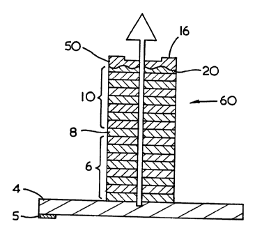
Figure 1 shows an embodiment of a polarising VCSEL (60) according to
a first embodiment of the present invention. The VCSEL (60) is grown
on a substrate (4) which includes the bottom electrical contact (5) of the
CA 02378457 2002-01-04
WO 01/05008 PCT/GBOO/02550
VCSEL and comprises a lower multi-layer Bragg stack or mirror (6), a
gain region (8) and an upper multi-layer Bragg stack or mirror (10). The
upper Bragg mirror (10) is partially reflecting and so light is emitted from
the VCSEL (60) from its upper surface. On the upper surface is formed
5 the top electrical contact of the VCSEL which is in the form of a
corrugated metal mirror (50) surrounded by an annular region (16). As is
well known in the art the gain region (8) consists of quantum wells.
Normally the thickness of each layer in each of the Bragg stacks (6,10)
are one quarter of the operating wavelength in the semiconductor
10 material (i.e. the wavelength in air divided by four times the refractive
index of the Bragg layer).
The substrate (4) is composed of Gallium Arsenide (GaAs) and the
layers of the lower and upper Bragg mirrors (6,10) are made from
alternating layers of Aluminium Arsenide (AlAs) and Aluminium Gallium
Arsenide (AlGaAs). The lasing region of the VCSEL (60) is defined by
the physical removal of material to form a small pillar which forms the
VCSEL (60) as is shown in Figure 1,. Alternatively the lasing region
could be defined by forming apertures using ion implantation or
oxidisation using a mask to render exposed regions electrically non-
conductive. The GaAs substrate (4) is transparent above a wavelength
of around 980nm (the actual cut-off wavelength depends on the doping
levels and materials in the substrate (4)). Above this wavelength the
VCSEL (60) can either be top emitting (as shown in Figure 1) or bottom
emitting. Below 980nm the VCSEL has to be top emitting.
Surface plasmon polaritons (SPPs) are surface electromagnetic waves
that propagate at the interface between a metal (in this case the metal
mirror (50)) and a dielectric (in this case the top layer (20) of the upper
Bragg mirror (10)). The SPP waves are transverse mode (TM)
polarised. The dispersion relation for SPPs is given by:
CA 02378457 2002-01-04
WO 01/05008 PCT/GBOO/02550
11
Kspp = KO[E1E2/(E1 + E2)1 1/2
where KSPP is the surface plasmon wave vector
Ko is the wave vector of a photon in free space with the
same frequency, and
E1 and E2 are the real parts of the relative permittivities of
the metal and the dielectric respectively.
The dispersion relation of in-plane wave vector k, against frequency co
for an SPP wave is shown by the solid line in Figure 5. The dotted line
in Figure 5 is called the light line and corresponds to the maximum in-
plane momentum of a photon in the dielectric, i.e. at grazing incidence.
Points to the left of the light line correspond to light propagating at some
angle to the plane of the grating. The kX=O line corresponds to light
incident normal to the grating.
It can be seen from the graph in Figure 5 that an SPP wave has a
greater wave-vector than that of aphoton of the same frequency
because the SPP wave line lies to the right of the light line in Figure 5.
In order to excite a SPP with incident light the momentum of the incident
photon must be enhanced to match the momentum of the SPP mode.
This can be achieved by the use of a grating. If the pitch Xc of the
grating comprising the corrugated mirror is chosen correctly, coupling
between the electromagnetic field of an incident photon and surface
charges can occur for light at normal incidence. When coupling occurs
the specular reflectivity of the grating is reduced. The coupling
efficiency is dependent on the grating amplitude and if chosen correctly
the reflectivity can be reduced to zero. This is only true however, if
there is a normal component of the electric field of the incident photon to
the surface of the metal, otherwise SPPs cannot be produced. Thus at
normal incidence only light polarised with the electric vector
CA 02378457 2002-01-04
WO 01/05008 PCT/GBOO/02550
12
perpendicular to the grating grooves will excite SPPs, the orthogonal
polarisation does not have a normal component of the electric vector to
the metal surface and so cannot generate the required surface charge.
Figures 2 and 3 show the corrugated surface (62) of the mirror (50)
which interfaces with the top layer (20) of the upper Bragg mirror (10) in
the embodiments of Figures 1 and 4 and which interfaces with the air
above the VCSEL in the embodiment of Figure 6. The reflectivity of the
grating (50) will fall to zero for the case shown in Figure 2 in which the
electric field vector (E) of incident light of polarisation p, from within the
VCSEL is perpendicular to the grating grooves (52) if the amplitude of
the grating is chosen correctly. When the electric field vector (E) of
incident light from within the VCSEL of orthogonal polarisation P2 is
parallel to the grating grooves (52), there is no normal component as
shown in Figure 3. Consequently, in the situation shown in Figure 3
SPPs cannot be excited and the reflectivity of the grating (50) is close to
100%. Thus, the mirror (50) acts as a differential absorber for
orthogonal polarisations of incident light.
The pitch kc of the grating comprising the corrugated mirror (50)
required to achieve coupling is given by the following momentum
matching condition:
27C/?IG = Kspp
The VCSEL (52) of Figure 4 is a bottom emitting VCSEL. The VCSEL
(52) emits light represented by arrow (54) through the substrate (4). A
thick corrugated metal mirror (50) is located at the top of the upper
Bragg mirror (10) which also forms the top electrode of the VCSEL. The
metal mirror (50) is corrugated such that when the E field of incident
light is parallel to the grooves in the mirror (50) (ie. in a polarisation P2)
the reflectivity of the mirror (50) is close to 100%. However, when the E-
CA 02378457 2002-01-04
WO 01/05008 PCT/GBOO/02550
13
field of incident light is perpendicular to the grooves in the mirror (50)
(ie. in orthogonal polarisation pi) the reflectivity of the mirror (50) is
substantially reduced and light of this second polarisation is absorbed in
the mirror (50) and thus lost from the cavity of the VCSEL (52). Thus, at
the threshold current of the VCSEL (52) the VCSEL (52) will lase at a
polarisation with its E field parallel to the grooves in the mirror (50).
Figure 1 shows an alternative to the embodiment shown in Figure 4
which is top emitting. In this case the metal mirror (50) on the top of the
upper Bragg mirror (10) has a thickness which is small enough to allow
some light of polarisation p, to be transmitted through it. It may be
necessary to decrease the number of layers in the upper Bragg mirror
(10) to achieve the desired level of transmission.
Alternatively the thickness of the top Bragg layer (20) can be chosen
such that the strong reflection for light_ polarised with the electric vector
parallel to the grating grooves destructively interferes with the reflections
from the rest of the Bragg stack, thus reducing the overall reflectivity,
and hence reducing the gain for this polarisation. Light polarised
orthogonal to this with the electric vector perpendicular to the grating
grooves is simply absorbed by the grating structure (i.e. excites SPPs).
However the reflectivity of the overall mirror is still high due to the rest
of
the Bragg stack, and hence lasing will occur for the light polarised with
the electric vector perpendicular to the grating grooves.
A more practical alternative to those of Figures 1 and 4 is shown in
Figure 6 with like parts denoted by the same numerals. In the VCSEL
(80) of Figure 6 the corrugated surface of the mirror (50) is uppermost
and interfaces with the air above the VCSEL (80). In this way SPPs are
excited by light travelling through the mirror (50) (which must be thin
enough for light to pass through it) from within the VCSEL (8) at the
metal/air interface of the corrugated mirror (50). In this case the pitch of
CA 02378457 2002-01-04
WO 01/05008 PCT/GB00/02550
14
the mirror grating would be slightly less than the operating wavelength in
air and so is much easier to fabricate.
The second embodiment shown in Figures 7 and 8 comprises a VCSEL
(90) with like parts identified by the same numerals as in Figures 1, 4
and 6. The VCSEL (90), the top part of which is shown in Figure 7
comprises an upper Bragg stack (10) with a diffraction grating (92)
formed on or alternatively in its upper surface. The reflecting properties
of the grating (92) are demonstrated schematically in Figure 8.
Part of an incident beam of light (94) from the Bragg stack (10) (shown
in dotted lines in Figure 8) is reflected by the upper surface of the
grating (92) to produce a beam (96) which propagates back into the
Bragg stack (10). However, the upper surface of the grating (92) is
suitably corrugated so that part of the incident beam (94) is diffracted at
the interface between the upper surface of the grating (92) and the air
above it into a waveguide mode in the layer of grating as shown by light
beams (100,102). The light beams (100,102) in the waveguide mode
can also diffract from the interface between the upper surface of the
grating (92) and the air above it, back into the Bragg stack (10) to
produce a light beam (98). The relative phase between beams (96) and
(98) (and any successive diffracted waveguide mode beams) will be
determined by the phase shifts on reflection of the incident beam (96)
and waveguide mode beam (102) at the upper surface of the grating
(92), ~j and the phase shift on reflection of the waveguide mode beam
(100) at the lower surface of the grating (92) (where it interfaces with the
Bragg stack (10)), ~2, as well as the extra path length (2P) of the beams
(100,102) within the waveguide mode. If (2~1 +~2 + 2P) is a multiple of
Tc then the beams (96) and (98) will destructively interfere and so will
reduce the overall reflectivity of the top mirror of the VCSEL (90). The
path length 2P is determined by the angle of propagation of the beam
CA 02378457 2002-01-04
WO 01/05008 PCT/GBOO/02550
(100) (ie. by the pitch of the corrugations in the upper surface of the
grating (92)) and by the thickness of the grating layer (92). The phase
shifts ~j andJZ are determined by the angle of propagation of the beam
(100) and also by the polarisation of the incident beam (94). Thus, the
5 grating pitch can be chosen so that it reduces the reflectivity of the top
mirror of the VCSEL (90) for one polarisation of incident light (eg. (TM)
polarisation where the E-field is perpendicular to the grooves in the
grating (92)) whilst maintaining high reflectivity for the orthogonal
polarisation (in this example (TE) polarisation). If the difference
10 between the reflectivity of the upper mirror for the two modes is greater
than a few percent, then the VCSEL (90) will lase with modes polarised
in the direction that has the highest reflectivity (in this example the TE
polarisation).
15 The result from theoretical modelling of the top Bragg mirror (using
rigorous coupled wave theory) of the VCSEL shown in Figure 7 is shown
in Figure 9. A grating pitch was chosen so that with TM polarisation a
mirror with reduced reflectivity at normal incidence is produced, whilst
for the TE polarisation the reflectivity remains high at the operating
wavelength of 840nm at which the VCSEL is designed to operate. For
this model in the structure in Figure 7, there are 38 alternating layers of
AlAs (n=2.971, k=0.0001) and AIo.12Ga0778As (n=3.505, k=0.0001) which
are 70.68nm and 59.9nm thick respectively (ie. k/4) grown on a GaAs
substrate. The top grating layer is 266nm thick and is corrugated on
its top surface with a sinusoidal relief grating with a maximum depth of
106nm. Thus, the VCSEL (90) would lase with the E-field pointing along
the grating groves (TE polarisation). The corrugations in the grating
layer (92) could be produced holographically in a photo-resist layer
which could be spun on top of the top layer of the VCSEL. The
corrugations could then be transferred into the semiconductor layer (92)
by a suitable etching process.