Note: Descriptions are shown in the official language in which they were submitted.
CA 02379077 2002-O1-14
Interference-optical narrowband filter
The invention relates to an interference-optical narrowb~and filter for a
wavelength of ~,o with a great number of dielectric layer;~, as set out in the
preamble of Claim 1, as well as to the use of such filter and a plasma-
activated CVD process for the production of such narrowband,
interference-optical filters.
Narrowband, dielectric filters of Fabry-Perot design are known in prior art
from a large number of publications.
Reference is made in this respect to the following patent specifications:
US-4756602
CA 222091
WO 97/017777
EP 092305
The subject-matter of these patent specifications is included to the full
extent in the specifications of this application.
Interference-optical narrowband filters are produced by i:he alternating
application of high and low-refractive-index layers of a precisely defined
thickness of layer. The Fabry-Perot design has a symmetrical buildup
composed of 7~I4 layers around a so-called spacer layer (~,I2 or n*~,12
layer) - a so-called cavity -, which means that the arrangement of the
layers in the first half of a cavity is repeated in the second half in a
mirror-
inverted manner. The narrow-band filter consists of several
cavities, for example of three cavities. The expansion of the 7~I2 or ~,,I4
CA 02379077 2002-O1-14
layers is monitored and controlled during the production preferably with
the help of optical methods. The increase of the layer may be purposively
controlled, for example, by an extreme-value turn-off that interrupts the
coating process at precisely the point when the transmi:~sion or reflection
of the layering system reaches an extreme value, i.e. when the coating
thickness corresponds to a a,14 layer or an integral multiple thereof. In
order to produce a specified filter characteristic with the help of the
traditional deposit, i.e. from a great number of ~,,I4 layer's and a specified
selection of materials (i.e. a specified refractive index), an "oversizing" of
the layering system is frequently necessary. This means that very many
layers or very thick layers have to be used. This in turn means an
extension of the production time of the filters and, consE:quently, results in
most cases in less profitability.
An optical narrowband filter is known from US 4 756 60;2 in which the
spacer layers are separated into thinner layers by breaking them down
into equivalent layers of the same optical thickness in total.
The interference filter, as set out in US 4 756 602, was produced with the
help of a continuous vapor deposition technique by way of laser
ellipsometric layer-thickness control wherein, after the preposition of the
layer, its precise thickness was determined and the subsequent layer was
re-optimized. Such layer-thickness control is very expensive and can only
be used conditionally in practical operation.
It is the task of the invention to make available a very narrowband Fabry-
Perot filter with specified transmission characteristics without having to
tolerate the disadvantages according to the state of the art. The aim is to
2
CA 02379077 2002-O1-14
produce especially a narrowband interference filter of small total
thickness, if possible.
The problem is solved, according to the invention, by the fact that in an
interference-optical narrowband filter for a wavelength crf ~,o a number of
layers of a multilayered system have an optical thickness of layer that
deviates from 7~I2 or 714.
Such optical narrowband filter comprises, therefore, altE:rnately arranged
dielectric layers consisting, for example, of materials such as titanium
dioxide and silica, preferably nioboxide and silica, and wherein the optical
thickness of the individual layers can be any fraction or multiple of ~,/4.
Such design, according to the invention, has the advantage that at a
smaller total thickness than in designs consisting only of ~,/4 layers, a
respective transmission characteristic that conforms to predetermined
specifications can be achieved.
Preferred materials to be used for high-refractive-index layers are Nb20 5,
Ti0 2, Ta 20 5, Zr02 as well as Hf02.
For designs, according to the state of the art, with mirror coatings of (HL)-
stacks (H: coating made of a high-refractive-index material, L: coating
made of a low-refractive-index material), as well as spacer layers
consisting of n*~,/2 layers for which the coating materials have been
specified, it is not possible to adapt at will the transmission characteristic
to predetermined specifications since the ratio of the rE:fractive values, the
minimum reflection of the mirror coatings and the position of the band-
pass on the wavelength scale are very limited.
CA 02379077 2002-O1-14
The designs, according to the invention, overcome this disadvantage.
Furthermore, by using layers whose optic thickness deviates from x,14 or
multiples thereof, the so-called non-x,14 layers, it is possible to vary and
particularly to minimize recesses in the transmission characteristic of the
band-pass filter, the so-called "ripples".
Provision has been made in a preferred embodiment of the invention to
the effect that the optical thickness of layers that deviatE: from ~,/4 or
from
x,12 is selected in such a way that the total thickness of layer of the
interference-optical narrowband filter is minimized when the transmission
characteristic is specified.
It is especially preferable if the interference-optical narrowband filter has
a
great number of stacks with several alternating high and low-refractive
-index layers. In a first embodiment provision can have been made for the
arrangement of a large number of reflecting ~,/4 layers in a stack and for at
least one layer whose optical layer of thickness deviate:> from x.14 or 7~,I2.
It is also possible to provide a stack in which the optical thickness of
almost all layers deviates from ~,/4.
In a particular embodiment spacer layers have been prcwided between the
stacks that can comprise one or several ?~/2 layers but ~~Iso layers of an
optical thickness that deviates from 7~I2.
Since the designs, according to the invention, are produced in production
processes, using customary measuring methods, such ~~s optical moni-
toring or the extreme-value turn-off, and thus lack the required accuracy,
CA 02379077 2002-O1-14
a process is also indicated that makes the production of such narrowband
filters possible. According to the invention, a plasma-activated CVD
(PICVD) process is used for this purpose wherein the production
parameters are selected in such a way that per microwave pulse, on
average, clearly less than one monolayer of the dielectric layer is
deposited on a substrate. Thus, by counting the pulses it is possible to set
a specified thickness of layer.
In such plasma-activated CDV process, for example, it is possible to de-
termine first of all the number N of the plasma pulses in order to obtain a
x,14 or x,12 layer. Furthermore, to produce a layer of an optical thickness
that deviates from ~,/4 or ~,,I2 , the number of plasma pulses in relation to
the predetermined number N can be increased or decreased by n, so that
a slightly thicker or thinner layer than a ~./4 layer is creai:ed.
Alternatively to this, the material used for the production of a 714 layer in
a
plasma-activated CVD process can be replaced by a material with slightly
deviating optical constants in order to produce a layer o~f a thickness that
deviates from ~,/4 and without negatively affecting the edge steepness of
the filter since, the change-over to the other material can be made during
a pulse interval.
It is especially preferable when per plasma pulse, on average, clearly less
than one monolayer of the dielectric layer is deposited. A specified thick
ness of layer can then be very precisely set by counting the pulses.
A modification of the optical thickness of layer is possible by changing the
process parameters, such as the temperature of the substrate and/or the
gas pressure of the process or the coating rate.
CA 02379077 2002-O1-14
By changing the temperature of the substrate andlor the. gas pressure of
the process or the coating rate, differences in refractive values of 0.05 and
more can be obtained.
Described below are exemplified embodiments of Fabry-Perot narrow-
band filters that comprise one or several layers of a thiclkness deviating
from x,14.
Figure 1 shows a first, desired transmission curve of a layered
system.
Figure 2 shows the refractive-value path of a system that fulfills the
first, desired transmission curve with a total of 112 layers,
including a great number of layers whose ~nptical thickness
of layer deviates from x,14.
Figure 3 shows a second, desired transmission curve for a narrow-
band interference filter.
Figure 4 shows a transmission curve with a layered system of a
total of 66 layers, including a great numbE:r of layers whose
thickness of layer deviates from 7,.I4, and Having a total
thickness of approximately 16 pm, which almost meets the
desired values according to Figure 3.
Figure 5 shows the refractive-value path of the sysi:em according to
Figure 4.
6
CA 02379077 2002-O1-14
Fig. 6 shows the transmission curve of a layered system based on
~,/4 and ~./2 layers which almost meets the desired values
according to Figure 3. The system consisl.s of 78 layers of a
total thickness of approximately 27 Nm.
Fig. 7 shows the refractive-value path of the system according to
Fig. 6.
Figure 2 shows the refractive-value path of a system, according to the
invention, that closely reflects the path of the first desired transmission
curve, and which comprises a great number of layers the optical thickness
of which deviates from ~,I4 or ~,/2. The system consists of 112 layers in
total with the following build-up:
0.6505H, 034L 0.4243H 0.9405L 1.0015H 1.0113L "1.0043H 0.9935L
0.9838H 0.9778L 0.9776H 0.9831 L 0.9904H 0.99541_ 0.9971 H
0.9979L 1.0004H 4,0062L 1.0023H 1.0L 0.9982H 0.9966L 0.995H
0.9933L 0.9913H 0.9891 L 0.9869H 0.985L 0.9839H 0.9846L 0.9883H
0.9975L 1.0122H 09155L 0.0706H 0.1537L, 0.3915H, 0.2603L 0.7195H
1.0316L 1.0139H 0.9991 L 0.989H 0.9837L 0.9824H 0.9835L 0.9857H
0.9878L 0.9894H 0.9915L 0.9947H 0.9988L 1.0034H 4.0106L
1.0013H 0.9948L 0.9911 H 0.9893L 0.9883H 0.98771_ 0.9874H
0.9875L 0.9879H 0.9886L 0.9897H 0.9913L 0.9939f-~ 0.9981 L
0.8754H 0.0574L 0.1429H 0.8937L 0.0675H 0.1481 L. 0.3561 H
0.2993L 0.6967H 1.0004L 0.9846H 0.9745L 0.96971-I 0.9695L
0.9731 H 0.979L 0.9851 H 0.99L 0.9932H 0.9959L 0.9992H 1.0015L
1.0012H 4.0026L 0.9999H 1.0014L 1.0053H 1.009L 1.0065H
0.9933L 0.9723H 0.9523L 0.9413H 0.9428L 0.95451-I 0.9657L
0.9541 H 0.8887L 0.6238H 0.2241 L 0.1628H 0.6552L_ 0.0941 H
0.0149L
CA 02379077 2002-O1-14
In this connection H refers to a layer with a high refracti~re index nH , and
L
denotes a layer with a low index of refraction n~_ Prefer<~bly Nb205, Ti02,
Ta 20 5, Zr0 2 as well as Hf02 are used as materials for vrhe high-refractive-
index layers. The use of nioboxide is particularly preferred for the high-
refractive layer, whereas silica is especially preferred for the low-refrac-
tive-index layer. The optical thickness of layer is standardized as follows:
1,000=n~d=~,/4
which means a value of 1,000 corresponds to an optical thickness of layer
of exactly ~, /4; for example, a value of 0.9956 of an optical thickness of
layer that is slightly less than 7~ 14 and, for example, a value of 1.0043 of
an optical thickness of layer that is slightly greater than x,14.
In Fig. 2 a second desired characteristic for a narrow-bind interference
filter is specified.
Figures 4 and 5 show interference filters, according to the invention, that
fulfill to a large extent the required transmission path in conformity with
the
second desired characteristic as specified in Figure 3. I=figure 4 shows the
actual transmission path of an interference filter, according to the
invention. As can be seen from the comparison between Figure 3 and
Figure 4, the actual transmission path corresponds to s~ large extent to the
specified one, according to the second desired characteristic. The total
thickness of layer of the system, according to Fig. 4 and 5, is almost 50%
lower than the total thickness of layer of a system that is exclusively
comprised of 7~I4 and x,12 layers. Figure 5 shows the refractive path of the
invented system to fulfill the second desired characteristic. The system,
as shown in Fig. 5, consists of a total of 66 individual ladders with the
following build-up:
s
CA 02379077 2002-O1-14
0.5486H 0.007L 0.5289H 1.1718L 1.2095H 1.1575L 1.0469H 0.9728L
0.971 H 1.0217L 1.0764H 1.0379L 0.9368H 0.9652L 1.0171 H 0.9912L
0.945H 4.0895L 0.9593H 1.0102L 0.895H 0.9771 L 1.0412H 1.005L
0.9303H 0.8977L 0.9442H 1.0036L 1.032H 1.0729L 1.1511 H 1.175L
1.0713H 0.8283L 1.1149H 1.5524L 0.7855H 1.0895L_ 1.0185H 1.008L
1.0233H 1.0482L 1.0739H 1.1208L 1.2156H 0.93591_ 1.0174H
0.8977L 1.2226H 3.974L 0.8322H 0.986L 1.0412H 'I .1036L 0.9771 H
0.8995L 0.872H 0.8306L 0.8384H 0.928L1.0438H 1.115L 1.132H
1.1647L 1.2208H 1.3793L
The designations of the layered system are identical to those of the
system shown in Figure 1; this means L refers to layers of a low refractive
index and H refers to layers of a high refractive index. In the examples
given the refractive index of the high-index layer is n~= 1.43 and the
refractive index of the low-refractive-index layer is nH = ~'_.3. The
material of the high-refractive-index layer is preferably comprised of Nb20
5, and the material of the low-refractive-index layer preferably consists of
Si02. Figure 5 shows the refractive-index path in relation to the thickness
of layer. The alternation between high and low-refractive-index layers, as
well as the total of 2 spacer-like layers is clearly recognizable.
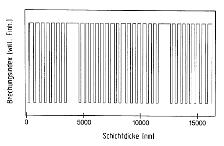
Figure 6 shows the transmission curve of a so-called three-cavity filter,
according to the state of the art, that is comprised exclusively of a,14 and
~,/2 layers, as well as multiples thereof. In this case stacks 1, 2, 5 and 6
are built up identically, and stacks 3 and 4 have mirror coatings consisting
of 3/4 7~-layers. A stack denotes a large number of a,14 I;~yers (or multiples
thereof) of alternating high and low-refractive-index materials. A cavity
comprises two stacks that are separated by spacer layers as, for example,
a x,12 layer made of high or low-refractive-index material. The coupling
5 layers between the individual cavities, for example, can be low-refractive
-index ~./4 layers.
9
CA 02379077 2002-O1-14
The design, according to the state of the art, likewise shows a good
approximation to the specified, second desired characteristic, as can be
seen from the comparison between Figure 3 and Figure 6.
As shown by the refractive-value path of the three-cavit~r filter, illustrated
in
Figure 7, the individual layers, as well as the two spacer layers are clearly
thicker in construction. This leads to an almost 50% greater total
thickness of layer in the state of the art, as compared to the design,
according to the invention.
Another advantage of the invention is the great edge stE:epness, as well
as a greater transmission in the passband width.
The illustrated, layered systems of an altered optical thickness are
produced preferably with the help of the plasma-activat~sd CVD process
as, for example, by applying an atomic monolayer or less per plasma
pulse and by counting the pulses as described above.
Alternatively, the optical thickness of layer can be altered by changing the
process parameters during the pulse interval that is variably adjustable.
The advantage of using the plasma-activated CVD process is the
achievement of a very effective change-over and the possibility within the
layered system to produce, in a simple way, layers of an optical thickness
that deviates from x,14. In current continuous CVD proccases this is not
possible without a change-over.
The very narrow-band ialters, produced according to the invention, whose
5 edge steepness is adjustable in a very controlled manner, can be used as
edge-type filters of extreme edge steepness or as very slat gain-flattening
filters. Furthermore, the introduced narrowband filters are suitable, due to
io
CA 02379077 2002-O1-14
their precisely controllable transmission path, for multiplexers or
demultiplexers in WDM (Wavelength-Division-Multiplex) or
in DWDM (Dense-Wavelength-Division-Multiplex) systems of
telecommunications engineering. A special advantage of this invenstion is
the greatly reduced total thickness of layer as compared to the
conventional design.
m