Note: Descriptions are shown in the official language in which they were submitted.
CA 02379506 2002-O1-15
WO 01/89754 PCT/EPO1/05666
1
ARC WELDING GENERATOR WITH INPUT VOLTAGE ADAPTING
REGULATOR STAGE
Technical Field
The present invention relates to an arc welding generator with input
s voltage adapting regulator stage.
Background Art
A typical diagram of an arc welder, according to the known art, is shown
in Figure 1 and is constituted by a rectifier stage 1 followed by a bank of
leveling capacitors 2, followed by an inverter block 3 with high-frequency
to electronic switches which drives a transformer 4.
The secondary winding of the transformer 4 is followed by a rectifier
stage S and has an inductor 6 for leveling the output current.
The arc forms between the inductor 6 and the common line of the
rectifier stage.
is The voltage applied to the inverter block 3 is the voltage being present
across the bank of leveling capacitors 2, which is supplied by the input
rectifier stage 1.
This means that the maximum voltage value being present across the
bank of capacitors 2 coincides with the peak value of the rectified voltage
ao being present in output to the rectifier stage 2.
In these conditions, the electronic switches of the inverter stage 3 must
be sized so as to be able to withstand such voltage peak value.
Obviously, in order to ensure the operation of the generator for supply
voltages that are higher than the nominal supply voltage it is necessary to
2s oversize, in terms of voltage, the electronic switches of the inverter,
with a
consequent overall efficiency loss of the generator.
This is necessary because it must be taken into account that the welder
may have to operate with power supplies in which the voltage can vary due
to reasons linked to the fact that the line is not controlled, that it is a
so building yard line, that at certain times of the day there can be
variations due
CA 02379506 2002-O1-15
WO 01/89754 PCT/EPO1/05666
2
to the disconnection of loads or because power is drawn from a stand-alone
generator driven by a motor.
The same problems can occur on very long lines, where resonance with
the inductors and the capacitors of the machine may occur.
s Clearly, the use of electronic switches capable of withstanding high
voltages entails a decrease in efficiency, because these electronic devices
suffer losses which increase as their maximum operating voltage increases.
If one also wishes to ensure the operation of the generator for supply
voltages lower than the nominal voltage without performance losses, i.e.,
to with an equal delivered power level, it is necessary to oversize the
electronic switches of the inverter in terms of current.
This occurs, for example, when considerable line drops occur in
distribution systems which are insufficient with respect to the connected
loads.
is This oversizing in terms of current entails an increase in the nominal
power of the switches and once again a loss . of overall efficiency of the
inverter stage that is sized thereon.
The above has led to the development of structures for arc welding
generators which adopt intermediate regulator stages which allow to obtain
Zo an input voltage for the inverter stage 3, present across the capacitor
bank 2,
which is stable while the voltage of the power supply of said generator
varies.
An example of the above is shown in Figure 2, which illustrates an
intermediate stage between the rectifier block 1 and the capacitor bank 2;
2s said intermediate stage is known as "boost" stage and is obtained by means
of an inductor 71, an electronic switch 72, and a diode 73.
This stage is able to stabilize a constant voltage across the capacitors 2
by means of an appropriate control device.
However, said stage can operate if the supply voltages that are present in
3o input to the block 1 have a peak value which is lower than the value of the
CA 02379506 2002-O1-15
WO 01/89754 PCT/EPO1/05666
3
stabilized voltage across the capacitor 2, but operation for higher voltage
values is not allowed.
This entails that, in order to ensure operation with high supply voltages,
the voltage that must be stabilized across the block 2 is high, and
s accordingly it is still necessary to oversize the electronic switches of the
inverter stage, in terms of voltage, even in the presence of a regulator
stage,
with the already noted consequences in terms of loss of efficiency.
Another known solution is shown in Figure 3, wherein the fundamental
element of the system is a voltage adapting stage 101 which is interposed
to between the rectifier block 102 and the capacitor bank 103.
Downstream of the capacitors 103, which have a leveling function, there
is a conventional inverter block 104, the adapter transformer 105, the
rectifier stage 106 and the inductor 107 at the output of which the arc 108
forms.
is The voltage adapting stage 101 is constituted by an electronic switch
109, by an inductor 110 and by a diode 111, which are connected as shown
in Figure 3.
A control device, not shown, allows to keep constant the voltage Vo
measured across the block of capacitors 103 as the voltage V;" measured at
ao the output of the rectifier stage 102 varies, both in the case of V;" > Vo
and
in the case of V;" < Vo.
Substantially, the control device acts on the opening and closure of the
switch 109, maintaining the indicated conditions.
In this circuit diagram, however, the voltage Vo is negative with respect
as to the voltage V;n and the cut-off voltage of the switch 109 and of the
diode
111 is V;n + Vo, which is high for high input voltages V;n.
This entails the use of components having high cut-off voltages, which
can entail losses in conduction and a non-optimum efficiency of the
adapting stage.
so Moreover, the value V;" + Vo for wide ranges of the input voltage can
CA 02379506 2002-O1-15
WO 01/89754 PCT/EPO1/05666
4
reach values higher than the cut-off capacity of the devices normally used in
these machines, with the consequent need to use series-connected
components; this can entail complications linked to the difficulty of
ensuring a symmetrical distribution of the voltages across said components.
s Disclosure of the Invention
The aim of the present invention is to provide a generator for welding
which solves or in any case greatly reduces the problems that have been
mentioned.
A consequent primary obj ect is to provide a welding generator which is
to capable of ensuring the operation of the generator without loss of
performance as the supply voltage varies, be it a three-phase or single-phase
voltage, over a wide range of values.
Another object is to provide a welding generator which is capable of
operating both with values that are lower than the nominal voltage and with
is values that are higher than the nominal voltage while maintaining a stable
voltage value across the capacitor bank.
Another object is to provide a welding generator which is structured so
as to allow optimum sizing of the electronic switches of the inverter stage
with the goal of improving the efficiency of this stage and therefore of the
2o entire generator.
Another object is to provide a welding generator in which it is possible to
optimize the sizing of the semiconductor devices that are contained in it and
in particular in the adapting stage, so as to achieve a high overall
efficiency
of the generator.
as This aim and these and other objects which will become better apparent
hereinafter are achieved by a welding generator with an input voltage
adapting regulator stage of the type that comprises an input rectifier stage,
a
bank of leveling capacitors, an inverter block, a transformer, a rectifier
stage
and an inductor downstream of which the arc forms, characterized in that
so said regulator stage has, in series at the output of said input rectifier
stage, a
CA 02379506 2002-O1-15
WO 01/89754 PCT/EPO1/05666
first controlled electronic switch to the output of which a first diode is
connected, said first diode being further connected to the common line, an
inductor, a second controlled electronic switch and a second diode being
present in series downstream of said first controlled electronic switch, the
s output of said inductor being connected between said inductor and the
common line, said second diode being connected to the bank of leveling
capacitors, said arrangement causing the voltage V;n measured at the output
of the input rectifier stage to have the same orientation as the voltage Vo
measured across the bank of leveling capacitors.
to Brief description of the drawings
Further characteristics and advantages of the invention will become
better apparent from the following detailed description of the prior art
already defined in the introduction and of some preferred but not exclusive
embodiments of the invention, illustrated in the accompanying drawings,
is wherein:
Figure 1 is, as mentioned, a diagram of a welding generator according to
the prior art;
Figure 2 is a view of a second type of electronic welder according to the
prior art, with a boost-type preregulator stage;
~o Figure 3 is a view of a third type of welding generator according to the
prior art, with a single-switch preregulator stage with voltage inverted
across the bank of capacitors;
Figure 4 is a diagram of a welding generator according to the invention,
with a preregulator stage of the double-switch type;
2s Figure 5 is a view of a further embodiment of the preregulator stage of
the double-switch type;
Figures 6, 7, 8 and 9 show the typical behaviors of the line current in
three-phase and single-phase machines provided according to the prior art
and according to the invention.
so Ways to carrying out the Invention
CA 02379506 2002-O1-15
WO 01/89754 PCT/EPO1/05666
6
With reference to the figures, it has already been mentioned that Figures
1, 2, and 3 are diagrams of welders according to the prior art.
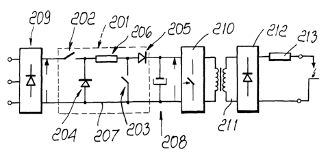
The invention in its basic form is shown in Figure 4.
In this diagram, the adapting stage, now designated by the reference
s numeral 201, has two electronic switches, designated by the reference
numerals 202 and 203 respectively, and two diodes, designated by the
reference numerals 204 and 205 respectively, and an inductor 206, all
arranged as shown in Figure 4.
Substantially, the diode 204 is connected between the output of the first
to switch 202 and the common line 207, the inductor 206 is arranged in series
to the output of the first switch 202, the second switch 203 is connected
between the output of the inductor 206 and the common line 207, while the
diode 205 is in series between the output of the inductor 206 and the block
of capacitors 208.
is As can be noted, in this arrangement the voltage Vo measured across the
block of capacitors 208 has the same orientation as the voltage Vin measured
at the output of the rectifier block, now designated by the reference numeral
209.
The switches 202 and 203, like the diodes 204 and 205, have an inverse
ao voltage across them, respectively V;" and Vo.
This allows to use components with optimum voltage characteristics,
with a consequent recovery in terms of efficiency of the adapting stage 201.
Figure 5 illustrates a further embodiment of the adapting stage, now
generally designated by the reference numeral 301.
as In this case there are again two electronic switches, designated by the
reference numerals 302 and 3'03 respectively, and two diodes 304 and 305,
but there are two inductors interposed in the common line 309, and at the
output line 310 of the rectifier stage, respectively, such inductors being now
designated by the reference numerals 306 and 307.
3o In this case also, the voltage V~, measured in output from the rectifier
CA 02379506 2002-O1-15
WO 01/89754 PCT/EPO1/05666
7
stage, not shown, has the same orientation as the voltage Vo measured
across the block of capacitors, now designated by the reference numeral
308.
Figures 6 and 8 show the typical behaviors of the absorption of line
s current for a single-phase and a three-phase generator, showing how the
typical absorption occurs with a high effective value due to the peaks of
current and to their harmonic content.
This absorption can be rendered substantially sinusoidal by using the
regulator according to the invention, appropriately controlled, thus making
to the generator equivalent to a resistive load.
The typical behaviors obtained by using the preregulator are plotted in
Figure 7 for a single-phase load and in Figure 9 for a three-phase load.
This allows not only to obtain line absorption with low harmonic
content, but also to optimize the sizing of the rectifier bridge in input,
since
is the current peaks are greatly reduced.
From what has been described and illustrated, it is evident that the
proposed aim and objects have been achieved and that in particular an arc
welding generator has been provided having a voltage adapting stage which
allows the single-phase and three-phase operation of the generator as the
Zo supply voltage varies over a wide range with respect to the nominal
voltage.
In this manner, optimization of the circuit allows to use components
which have optimum voltage characteristics, with a consequent recovery in
the efficiency of the stage per se and of the entire machine.
The inventive concept expressed and illustrated in the description and in
as the drawings can be provided in different forms while maintaining the same
operating logic.
The disclosures in Italian Patent Application No. PD2000A000136 from
which this application claims priority are incorporated herein by reference.