Note: Descriptions are shown in the official language in which they were submitted.
CA 02379621 2002-01-17
- 1 -
SPECIFICATION
APPARATUS AND METHOD FOR RECEIVING BS DIGITAL BROADCAST
Technical Field
[0001] This invention relates to an apparatus for receiving BS digital
broadcast
suitable for the receiving of the BS digital broadcast, and more particularly,
relates to an apparatus for receiving BS digital broadcast by which a stable
receiving operation is possible.
Background Art
[0002] The apparatus for receiving BS digital broadcast for receiving the BS
(Broadcasting Satellite) digital broadcast receives a signal transmitted by
the
time sharing by using a plurality of modulation techniques of multi-phase PSK
modulations such as 8 PSK (Phase Shift Keying) modulation, QPSK (Quadrature
PSK) modulation, or BPSK (Binary PSK) modulation in the way of time sharing.
The apparatus for receiving BS digital broadcast regenerates the carrier by
detecting the phase error of the received signal, and demodulates the digital
signal.
[0003] Conventionally, the apparatus for receiving BS digital broadcast which
regenerates the carrier by using a single demodulator circuit switches the
receiving operation according to the magnitude of the CNR in the received
signal.
For example, when the CNR is large (at the time of a high CNR), it performs
continuous receiving while responding all modulation techniques, and detects
the phase error and regenerates the carrier. On the other hand, when the CNR
is approximately in the middle degree (at the time of a medium CNR), it
performs
CA 02379621 2002-01-17
- 2 -
burst receiving of a signal subjected to the QPSK modulation and a signal
subjected to the BPSK modulation and detects the phase error, and regenerates
the carrier. Furthermore, when the CNR is small (at the time of a low CNR), it
performs burst receiving of a signal subjected to the BPS modulation and
detects
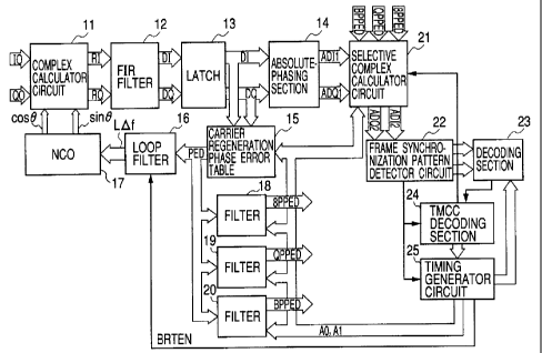
the phase error, ad regenerates the carrier.
[0004] Figure 3 is a drawing indicating one example of the structure of such a
conventional apparatus for receiving BS digital broadcast.
[0005] Here, when performing the burst receiving of a signal, for example,
such
an operation of holding the output of a loop filter 106 during the term when a
signal which cannot detect the phase error arrives is performed.
[0006] Furthermore, The apparatus for receiving BS digital broadcast switches
the receiving operation according to a switching instruction signal generated
by a
decoding section 109.
[0007] The decoding section 109 monitors the error rate or the like after
performing the trellis decoding or the like (Viterbi decoding in the case of
QPSK
or BPSK), and when the error rate or the like becomes a previously determined
value, it generates a switching instruction signal for instructing the
switching of
the receiving operation.
Problems to be Solved by the Invention
[0008] In the above described conventional apparatus for receiving BS digital
broadcast, in the case where the performance of a frequency converter of the
outdoor unit (general term made by integrally grasping an antenna and a down
CA 02379621 2002-01-17
- 3 -
converter) is not sufficient, when the receiving operation is switched, the
limit
CNR may change, which is the point where the correction becomes impossible
when the demodulated digital signal is coded to a connected code or the
correction is performed by an error correction code.
[0009] Figure 4 shows the limit CNR characteristic at the time of continuous
limit
receiving of 8PSK and BPSK to the phase noise characteristic of a local
oscillator
of the down converter in the outdoor unit (ODU).
[0010] According to this, the limit CNR characteristic a of the 8PSK and the
limit
CNR characteristic c of the BPSK in the continuous receiving at the time of a
high
CNR change to the limit CNR characteristics b, d in the burst receiving at the
time
of a medium CNR, respectively.
[0011 ] Therefore, the CNR at the switching point when switching the receiving
operation is different, and there has been such a problem that a hysteresis is
caused in the receiving operation.
[0012] From this point of view, it is also considered to detect the degree of
the
phase noise of the ODU or the like, since the fluctuation of the CNR at the
switching point is affected by the phase noise of the ODU or the like, but
this is
technically very difficult. Furthermore, even if that can be detected, it is
not sure
to prevent all hystereses from occurring.
[0013] This invention is made due to the above described actual situation, and
it
is an object to provide an apparatus for receiving BS digital broadcast by
which
the stable receiving operation is made possible.
CA 02379621 2002-01-17
4 -
Disclosure of the Invention
[0014] In order to attain the above described object, the apparatus for
receiving
BS digital broadcast of the present invention operates such that when it
regenerates the carrier by the carrier regeneration loop and establishes the
phase synchronization and decodes the PSK modulation signal regenerated from
the modulated signal to a digital signal, it shifts the phase of a signal
point
indicated by the PSK modulation signal outputted from the carrier regeneration
loop, by the phase determined on the basis of the type of the PSK modulation
technique applied to the received signal and the phase error contained in the
PSK modulation signal, and then, it decodes the digital signal, and performs
burst receiving only in a specified signal interval, and regenerates the
carrier on
the basis the detected phase error.
[0015] According to the present invention, it is possible to shift the phase
of the
signal point indicated by the PSK modulation signal outputted from the carrier
regenerating loop, by the phase determined on the basis of the type of the PSK
modulation technique applied to the received signal and the phase error
contained in the PSK modulation signal. Consequently, in the burst receiving,
it
is possible to reduce the effect on the error rate because of the phase noise
of
the ODU, and the stable receiving operation becomes possible by performing the
burst receiving at all times regardless of the magnitude of the CNR and
regenerating the carrier.
[0016] More particularly, in the case of the apparatus for receiving BS
digital
broadcast of the present invention, the carrier regenerating means comprises:
a
waveform data generator circuit for generating waveform data indicating the
CA 02379621 2002-01-17
- 5 -
regenerated carrier; a complex calculator circuit for performing complex
calculation of waveform data generated by the above described waveform data
generator circuit and a PSK modulation signal regenerated from the modulated
signal; a band limiting filter for limiting a band of a PSK modulation signal
in
which the phase of a signal point is adjusted by complex calculation of the
above
described complex calculator circuit; a latch circuit for latching a PSK
modulation
signal in which the band is limited by the above described band limiting
filter; an
error detector circuit for detecting a phase error by comparing the phase of a
signal point indicated by a PSK modulation signal latched by the above
described latch circuit with an absolute phase; and a loop filter for
smoothing an
error signal indicating the magnitude of a phase error detected by the above
described error detector circuit, and for supplying it to the above described
waveform data generator circuit.
[0017] Furthermore, it has a plurality of filter circuits for filtering the
error signal
indicating the magnitude of the phase error detected by the above described
error detector circuit only in the signal interval corresponding to the type
of the
PSK modulation technique applied to a received signal, and is characterized in
that the above described phase shift means shifts the phase of a signal point
indicated by the PSK modulation signal, by a phase corresponding to the error
signal filtered by the above described plurality of filter circuits.
[0018] Furthermore, more preferably, the above described decoding means has
control data decoding means for decoding data indicating the multiplex
structure
of a frame formed by the decoded digital signal from a PSK modulation signal,
and identification signal generating means for generating a modulation
identification signal indicating the PSK modulation technique applied to a
CA 02379621 2002-01-17
- 6 -
received signal identified by data decoded by the above described control data
decoding means, and the above described plurality of filter circuits receive
the
modulation identification signal generated by the above described
identification
signal generating means and identify the type of the PSK modulation technique
applied to a received signal, and the above described phase shift means
selects
the error signal filtered by the above described plurality of filter circuits,
according
to the PSK modulation technique identified from the modulation identification
signal generated by the above described identification signal generating
means,
and shifts the phase of a signal point indicated by the PSK modulation signal,
by
a phase corresponding to the selected error signal.
[0019] Furthermore, the apparatus of the present invention has pattern
detecting
means for detecting a frame synchronization pattern from the PSK modulation
signal in which the phase is shifted by the above described phase shift means,
and is characterized in that the above described absolute-phasing means
absolute-phases the PSK modulation signal, according to whether the frame
synchronization pattern detected by the above described pattern detecting
means is reversed.
[0020] The present invention can also be grasped as a method for receiving
digital broadcast.
[0021] In that case, the method for receiving BS digital broadcast of the
present
invention is characterized in that it comprises: a step of regenerating a
carrier by
a carrier regenerating loop and establishing synchronization; a step of
decoding
a digital signal from a PSK modulation signal; a step of decoding a digital
signal
after shifting the phase of a signal point indicated by the PSK modulation
signal
CA 02379621 2002-01-17
- 7 -
outputted from the above described carrier regenerating loop, by a phase
determined on the basis of the type of a PSK modulation technique applied to a
received signal and the phase error contained in the PSK modulation signal;
and
a step of regenerating a carrier on the basis of a phase error detected by
performing burst receiving only in a specified signal interval.
Brief Description of the Drawings
[0022] Figure 1 is a drawing exemplifying the frame structure in the
hierarchical
modulation technique;
[0023] Figure 2 is a drawing indicating the structure of an apparatus for
receiving
BS digital broadcast according to an embodiment of this invention;
[0024] Figure 3 is a drawing indicating the structure of a conventional
apparatus
for receiving BS digital broadcast; and
[0025] Figure 4 is a drawing for explaining the fluctuation of the limit CNR
to the
phase noise characteristic the ODU because of the switching of the receiving
operation of the conventional apparatus for receiving BS digital broadcast.
Best Mode for Carrying Out the Invention
[0026] An apparatus for receiving BS digital broadcast according to an
embodiment of this invention will be described below in detail by referring to
drawings.
[0027] This apparatus for receiving BS digital broadcast receives an In-phase
signal 10 and a Quadrature-phase signal QO of the base band outputted by
CA 02379621 2002-01-17
- 8 -
subjecting the BS-IF (Broadcasting Satellite-Intermediate Frequency) signal
that
is a modulated signal made of a received radio wave down converted by an
outdoor unit (ODU) or the like, to quasi-synchronous detection with a
quadrature
detector. Each of the In-phase signal 10 and the Quadrature-phase signal QO
received by this apparatus for receiving BS digital broadcast is a PSK (Phase
Shift Keying) modulation signal including an In-phase component and a
Quadrature-phase component of a carrier included in the modulated signal.
Hereafter, for the sake of convenience, the In-phase signal is called an I
signal
and the Quadrature-phase signal is called a Q signal.
[0028] In the case of the BS digital broadcast, the frame is constructed in
such a
way where a specified number of symbols is a unit, and a hierarchical
modulation
technique is used in the way of time sharing, which is made by combining a
plurality of modulation techniques with different necessary CNR values such as
TC8PSK (Trellis Coded 8PSK) modulation, QPSK (Quadrature PSK) modulation,
and BPSK modulation. Furthermore, into the digital signal transmitted by the
BS
digital broadcast, a burst symbol is inserted, which makes the demodulation
possible when a CNR (Carrier-to-Noise Ratio) is small (at the time of a low
CNR).
[0029] Figure 1 is a drawing exemplifying the frame structure in the
hierarchical
modulation technique used in the BS digital broadcast.
[0030] In the case of the frame indicated in Figure 1, one frame is made up of
39936 symbols, and it includes a header part HE made of 192 symbols, a main
signal part 30 of 203 symbols constructed as a plurality of pairs, and a burst
symbol part 31 of four symbols.
CA 02379621 2002-01-17
- 9 -
[0031 ] The header part HE includes a frame synchronization pattern W1, TMCC
(Transmission and Multiplexing Configuration Control) data TD, and a super
frame identification pattern W2 (or W3).
[0032] The frame synchronization pattern W1 uses specified 20 bits among 32
bits and it is one for transmitting a unique word for establishing the frame
synchronization. Supposing that this unique word for establishing the frame
synchronization is (S19S18S17 SISO), (S19S18S17 ...
S 1 So) = (11101100110100101000) is made.
[0033] The TMCC data TD is data of 128 symbols indicating the multiplexing
configuration or the like of the modulation technique multiplexed by the time
sharing.
[0034] The super frame identification pattern W2 is one for identifying the
head of
the super frame made of eight frames, and uses specified 20 bits in the
pattern of
32 symbols. Furthermore, in the header part HE corresponding to seven frames
other than the head, a super frame identification pattern W3 made by reversing
the super frame identification pattern W2 is included.
[0035] The main signal part 30 is subjected to the modulation by any one or
more
of modulation technique among TC8PSK modulation, QPSK modulation, and
BPSK modulation, and is sent by the way of time sharing by the frame as a
unit.
[0036] The burst symbol part 31 is a PN (Pseudo Noise) signal which is
subjected to the modulation by the BPSK modulation technique and is reset for
each frame.
CA 02379621 2002-01-17
- 10 -
[0037] In order to receive the BS digital broadcast using such a hierarchical
modulation technique, as indicated in Figure 2, the apparatus for receiving BS
digital broadcast according to the embodiment of this invention includes a
complex calculator circuit 11, an FIR filter 12, a latch 13, an absolute-
phasing
section 14, a carrier regeneration phase error table 15, a loop filter 16, an
NCO
(numerical control frequency oscillator) 17, first to third filters 18 to 20,
a selective
complex calculator circuit 21, a frame synchronization pattern detector
circuit 22,
a decoding section 23, a TMCC decoding section 24, and a timing generator
circuit 25.
[0038] The complex calculator circuit 11 is made of a reversing circuit and a
multiplier circuit or the like, and performs calculation for eliminating the
phase
error and the frequency error included in the I signal 10 and the Q signal QO.
[0039] More particularly, the complex calculator circuit 11 applies the
reversing
processing or the like to the sine wave data sinO received from the NCO 17,
and
after that, multiplies it with the I signal 10 and Q signal QO to generate the
I signal
RI and Q signal RQ.
[0040] The complex calculator circuit 11 sends the generated I signal RI and Q
signal RQ to the FIR filter 12.
[0041] The FIR filter 12 is a roll off filter for limiting the pass band of
the I signal RI
and Q signal RQ received from the complex calculator circuit 11. The I signal
DI
and Q signal DQ passing through the FIR filter 12 are latched by the latch 13,
and
are supplied to the absolute-phasing section 14 and the carrier regeneration
phase error table 15.
CA 02379621 2002-01-17
- 11 -
[0042] The absolute-phasing section 14 is one for absolute-phasing the I
signal
DI and Q signal DO supplied from the latch 13 to generate the I signal ADI1
and
0 signal ADQ1, and sends the generated the I signal ADI1 and 0 signal ADQ1 to
the selective complex calculator circuit 21.
[0043] The carrier regeneration phase error table 15 identifies the signal
point
position in the signal space (I-Q vector plane) on the basis of the I signal
DI and
Q signal DQ supplied from the latch 13, and generates a phase error signal PED
indicating the phase error of the phase indicated by the signal point position
and
the absolute phase.
[0044] The phase error signal PED generated by the carrier regeneration phase
error table 15 is smoothed in the loop filter 16, and is supplied to the NCO
17 as
a phase adjustment signal Lef. Furthermore, the phase error signal PED is
smoothed in the first to third filters 18 to 20, and after that, it is
supplied to the
selective complex calculator circuit 21.
[0045] The NCO 17 generates the sine wave data sinO and cosine wave data
cosO that are waveform data to be accumulated corresponding to the phase
adjustment signal LMf supplied from the loop filter 16, and sends them to the
complex calculator circuit 11.
[0046] Each of the first to third filters 18 to 20 is one for smoothing the
phase
error signal PED sent from the carrier regeneration phase error table 15.
[0047] The first filter 18 filters the phase error signal PED sent from the
carrier
regeneration phase error table 15 during the period when the TC8PSK
CA 02379621 2002-01-17
- 12 -
modulation is applied to the received signal to generate an eight-phase phase
error signal 8PPED. The first filter 18 sends the generated eight-phase phase
error signal 8PPED to the selective complex calculator circuit 21, in turn.
[0048] The second filter 19 filters the phase error signal PED sent from the
carrier
regeneration phase error table 15 during the period when the QPSK modulation
is applied to the received signal to generate a four-phase phase error signal
QPPED. The second filter 19 sends the generated four-phase phase error
signal QPPED to the selective complex calculator circuit 21, in turn.
[0049] The third filter 20 filters the phase error signal PED sent from the
carrier
regeneration phase error table 15 during the period when the BPSK modulation
is applied to the received signal to generate a two-phase phase error signal
BPPED. The third filter 20 sends the generated two-phase phase error signal
BPPED to the selective complex calculator circuit 21, in turn.
[0050] The selective complex calculator circuit 21 performs the calculation
for
adjusting the phase of a signal point indicated by the I signal ADI1 and Q
signal
ADQ1 received from the absolute-phasing section 14.
[0051 ] More particularly, the selective complex calculator circuit 21
identifies the
modulation technique (TC8PSK, or QPSK, or BPSK) applied to the received
signal by the modulation identification signals A0, Al received from the
timing
generator circuit 25. The selective complex calculator circuit 21 generates
the I
signal ADI2 and 0 signal ADQ2 in which the phase of a signal point is shifted
by
the phase corresponding to the eight-phase phase error signal 8PPED, or the
four-phase phase error signal QPPED, or the two-phase phase error signal
CA 02379621 2002-01-17
- 13 -
BPPED received from the first to third filters 18 to 20 according to the
identified
modulation technique. The selective complex calculator circuit 21 sends the
generated I signal ADI2 and Q signal ADQ2 to the frame synchronization pattern
detector circuit 22.
[0052] Furthermore, when the TMCC decoding section 24 cannot decode the
TMCC data TO, the selective complex calculator circuit 21 sends the I signal
ADI1
and Q signal ADQ2 received from the absolute-phasing section 14 to the frame
synchronization pattern detector circuit 22 as the I signal ADI2 and Q signal
ADQ2 as they are, respectively.
[0053] Furthermore, even if the absolute-phasing section 14 is provided
between
the selective complex calculator circuit 21 and the frame synchronization
pattern
detector circuit 22, there is an effect similar to that in the case where it
is provided
between the latch 13 and the selective complex calculator circuit 21.
[0054] The frame synchronization pattern detector circuit 22 is one for
detecting a
frame synchronization pattern W1 included in the digital signal transmitted by
using the hierarchical modulation technique, and sends a signal indicating the
timing at which the frame synchronization pattern W1 is detected to the TMCC
decoding section 24 and the timing generator circuit 25.
[0055] Furthermore, the frame synchronization pattern detector circuit 22
sends a
signal indicating whether the detected frame synchronization pattern W1 is
reversed or not to the absolute-phasing section 14.
CA 02379621 2002-01-17
- 14 -
[0056] Furthermore, the frame synchronization pattern detector circuit 22
sends
the I signal ADI2 and Q signal ADQ2 received from the selective complex
calculator circuit 21 to the decoding section 23.
[0057] The decoding section 23 is one for decoding the digital signal for BS
digital broadcast, on the basis of the I signal ADI2 and Q signal ADQ2
received
from the frame synchronization pattern detector circuit 22. At this moment,
the
decoding section 23 extracts the TMCC data TD in the digital signal, and sends
that to the TMCC decoding section 24.
[0058] The TMCC decoding section 24 is one for decoding the TMCC data TD
received from the decoding section 23 to identify the frame structure
(multiplexing structure) of the received signal. The TMCC decoding section 24
sends a signal for giving notice of the identified frame structure to the
timing
generator circuit 25. Furthermore, the TMCC decoding section 24 sends a
signal for giving notice of whether the TMCC data TD has been decoded or not
to
the selective complex calculator circuit 21.
[0059] The timing generator circuit 25 generates modulation identification
signals
A0, Al for identifying the modulation technique (TC8PSK, or QPSK, or BPSK)
applied to the received signal, on the basis of the signal received from the
frame
synchronization circuit pattern detector circuit 22 and the TMCC decoding
section 24. The timing generator circuit 25 sends the generated modulation
identification signals A0, Al to the selective complex calculator circuit 21
and the
first to third filters 18 to 20.
CA 02379621 2002-01-17
- 15 -
[0060] Furthermore, the timing generator circuit 25 generates a timing signal
BRTEN which instructs the switching of the filtering/holding operation for
performing burst-receiving, and sends it to the loop filter 16.
[0061 ] Furthermore, the timing generator circuit 25 generates a signal which
controls the de-mapping operation or the like at the time of restoring the
digital
signal, and sends it to the decoding section 23.
[0062] The operation of the apparatus for receiving BS digital broadcast
according to the embodiment of this invention will be described below.
[0063] This apparatus for receiving BS digital broadcast makes the stable
receiving operation possible, by deviating the phase of a signal point
indicated
by the I signal ADI1 and 0 signal ADQ1 which are absolute-phased after the
phase error or the frequency error have been eliminated by the carrier
regenerating loop by the phase corresponding to the modulation technique
applied to the received signal and the phase error amount.
[0064] In the case of this apparatus for receiving BS digital broadcast, a
complex
calculator circuit 11, an FIR filter 12, a latch 13, a carrier regeneration
phase error
table 15, a loop filter 16, and an NCO 17 make up a carrier regenerating loop
for
eliminating the frequency error of the carrier included in the I signal 10 and
Q
signal QO of the base band received from the quadrature detector or the like.
[0065] That is, first, the complex calculator circuit 11 receives the I signal
10 and
Q signal QO obtained by subjecting the BS-IF signal made by down converting
the received radio wave by the ODU (not indicated in the drawing) or the like
to
CA 02379621 2002-01-17
- 16 -
the quasi-synchronous detection with the quadrature detector (not indicated in
the drawing) or the like.
[0066] The complex calculator circuit 11 performs the calculation indicated in
Equation 1 by using the sine wave data sing and the cosine wave data cosh
received from the NCO 17, and generates the I signal RI and the Q signal RQ in
which the phases are adjusted.
[Equation 1 ]
RI=IOxcoso-QOxsinO
RQ=l0xsinQ+QOxcosO
[0067] The complex calculator circuit 11 inputs the generated I signal RI and
Q
signal RQ in the FIR filter 12 and limits the band, and makes them the I
signal DI
and Q' signal DQ. The I signal DI and Q signal DQ are latched by the latch 13,
and are supplied to the absolute-phasing section 14 and the carrier
regeneration
phase error table 15.
[0068] The carrier regeneration phase error table 15 identifies the signal
point
position in the signal space on the basis of the I signal DI and Q signal DQ
supplied from the latch 13, and generates a phase error signal PED indicating
the
phase error of the phase indicated by the signal point position and the
absolute
phase.
[0069] The carrier regeneration phase error table 15 sends the generated phase
error signal PED to the loop filter 16.
CA 02379621 2002-01-17
- 17 -
[0070] The loop filter 16 generates a phase adjustment signal LAf made by
smoothing the phase error signal PED while switching the filtering/holding
operation according to the timing signal BRTEN sent from the timing generator
circuit 25, and supplies it to the NCO 17.
[0071] The NCO 17 generates the sine wave data sin6 and the cosine wave data
cos8 to be accumulated (oscillated) corresponding to the phase adjustment
signal LAf, and sends them to the complex calculator circuit 11.
[0072] When the carrier is regenerated by such a carrier regenerating loop,
and
the phase synchronization is established, it becomes possible to detect the
frame
synchronization pattern W1 by the frame synchronization pattern detector
circuit
22, on the basis of the I signal ADI2 and the 0 signal ADQ2 outputted from the
selective complex calculator circuit 21 through the absolute-phasing section
14
from the latch 13.
[0073] Furthermore, at this moment, the decoding of the TMCC data TD by the
TMCC decoding section 24 has not been performed yet, and therefore, the
selective complex calculator circuit 21 sends the I signal ADI1 and the Q
signal
ADQ1 received from the absolute-phasing section 14 to the frame
synchronization pattern detector circuit 22 as they are as the I signal ADI2
and
the Q signal ADQ2.
[0074] Here, various types of modulation signals corresponding to the
hierarchical modulation technique used in the BS digital broadcast are
absolute-phased on the transmitting side. Accordingly, the frame
synchronization pattern detector circuit 22 can judge whether the receiving is
CA 02379621 2002-01-17
- 18 -
performed by the absolute phase or by the phase rotated by 180 degrees, by
detecting the frame synchronization pattern W1 transmitted by using the BPSK
modulation technique.
[0075] That is, when the receiving is performed by the absolute phase, the
frame
synchronization pattern detector circuit 22 detects the frame synchronization
pattern W1 as (S19S18S17 ... S1S0)=(11101100110100101000).
[0076] On the other hand, when the receiving is performed by the phase rotated
by 180 degrees, the frame synchronization pattern detector circuit 22 detects
the
frame synchronization pattern W1 as (S19S18S17 ...
S1So) _ (00010011001011010111) where the value of each digit is reversed.
[0077] The frame synchronization pattern detector circuit 22 sends a signal
indicating whether the value of each digit of the detected frame
synchronization
pattern W1 is reversed or not, that is, whether the receiving is performed by
the
absolute phase or by the phase rotated by 180 degrees, to the absolute-phasing
section 14.
[0078] When it is judged that the receiving is performed by the absolute phase
from the signal received from the frame synchronization pattern detector
circuit
22, the absolute-phasing section 14 sends the I signal DI and the Q signal DQ
supplied from the latch 13 to the selective complex calculator circuit 21 as
they
are as the I signal ADI1 and the Q signal ADQ2.
[0079] On the other hand, when it is judged that the receiving is performed by
the
phase rotated by 180 degrees from the signal received from the frame
CA 02379621 2002-01-17
- 19 -
synchronization pattern detector circuit 22, the absolute-phasing section 14
makes the phase of a signal point indicated by the I signal DI and the Q
signal
DQ supplied from the latch 13 the absolute phase, and sends the I signal
ADI1=(-1)xDl and the Q signal ADQ1=(-1)xDQ to the selective complex
calculator circuit 21.
[0080] Thus, when the frame synchronization pattern detector circuit 22
detects
the frame synchronization pattern W1 and establishes the frame timing, the
positions in terms of time series of the frame synchronization pattern W1, the
TMCC data TD, the super frame identification pattern W2 (or W3), and the burst
symbol part 31 become clear. The frame synchronization pattern detector
circuit 22 sends a signal indicating the timing at which the frame
synchronization
pattern W1 is detected to the TMCC decoding section 24 and the timing
generator circuit 25.
[0081] The TMCC decoding section 24 identifies the timing for receiving the
TMCC data, from the position in terms of time series of the frame
synchronization
pattern W1 identified by the signal received from the frame synchronization
pattern detector circuit 22, and obtains the reception data from the decoding
section 23 at the identified timing. The TMCC decoding section 24 decodes the
TMCC data TD from the reception data obtained from the decoding section 23,
and identifies the frame structure (multiplexing structure) of the received
signal.
The TMCC decoding section 24 sends the signal for giving notice of the
identified
frame structure to the timing generator circuit 25.
[0082] The timing generator circuit 25 generates the modulation identification
signals A0, Al for identifying the modulation technique (TC8PSK, or QPSK, or
CA 02379621 2002-01-17
- 20 -
BPSK) applied to the received signal, on the basis of the signal received from
the
frame synchronization pattern detector circuit 22 and the TMCC decoding
section
24.
[0083] Furthermore, when the phase error signal PED is generated, the carrier
regeneration phase error table 15 sends that to the first to third filters 18
o 20,
too.
[0084) Each of the first to third filters 18 to 20 identifies the modulation
technique
(TC8PSK, or QPSK, or BPSK) applied to the received signal, by the modulation
identification signals A0, Al received from the timing generator circuit 25,
and
filters the phase error signal PED according to the identified modulation
technique.
[0085] That is, when the identified modulation technique is TC8PSK, the first
filter
18 filters the phase error signal PED and generates an eight-phase phase error
signal 8PPED, and sends it to the selective complex calculator circuit 21.
[0086] On the other hand, when the identified modulation technique is QPSK,
the
second filter 19 filters the phase error signal PED and generates a four-phase
phase error signal QPPED, and sends it to the selective complex calculator
circuit 21.
[0087] Furthermore, on the other hand, when the identified modulation
technique
is BPSK, the third filter 20 filters the phase error signal PED and generates
a
two-phase phase error signal BPPED, and sends it to the selective complex
calculator circuit 21.
CA 02379621 2002-01-17
- 21 -
[0088] The selective complex calculator circuit 21 displaces the phase of a
signal
point indicated by the I signal ADI1 and the Q signal ADQ1 generated by
absolute-phasing the I signal DI and the 0 signal DQ by the absolute-phasing
section 14, by the phase corresponding to the phase error signal (eight-phase
phase error signal 8PPED, or four-phase phase error signal QPPED, or
two-phase phase error signal BPPED) generated by the filtering of the first to
third filters 18 to 20.
[0089] At this moment, the selective complex calculator circuit 21 selects a
phase
error signal corresponding to the modulation technique identified from the
modulation identification signals A0, Al received from the timing generator
circuit
25.
[0090] That is, when the modulation technique identified from the modulation
identification signals A0, Al is TC8PSK, the selective complex calculator
circuit
21 selects the eight-phase phase error signal 8PPED received from the first
filter
18.
[00911 On the other hand, when the modulation technique identified from the
modulation identification signals A0, Al is QPSK, the selective complex
calculator
circuit 21 selects the four-phase phase error signal QPPED received from the
second filter 19.
[0092] Furthermore, on the other hand, when the modulation technique
identified
from the modulation identification signals A0, Al is BPSK, the selective
complex
calculator circuit 21 selects the two-phase phase error signal BPPED received
from the third filter 20.
CA 02379621 2002-01-17
- 22 -
[0093] More particularly, when the selective complex calculator circuit 21
selects
the eight-phase phase error signal 8PPED, it generates the I signal ADI2 and
the
Q signal ADQ2 in which the phase of a signal point indicated by the I signal
ADI1
and the Q signal ADQ1 is shifted, by performing such a calculation as
indicated
in Equation 2 where 0,=8PPED.
[Equation 2]
ADI2=ADI1 xcos0,-ADQ1 xsin0,
ADQ2=AD11 xsin0, +ADQ1 xcos0,
[0094] On the other hand, when the selective complex calculator circuit 21
selects the four-phase phase error signal QPPED, it generates the I signal
ADI2
and the Q signal ADQ2 in which the phase of a signal point indicated by the I
signal ADI1 and the Q signal ADQ1 is shifted, by performing such a calculation
as indicated in Equation 3 where 02=QPPED.
[Equation 3]
ADI2=ADI1 xcos02 ADQ1 xsin02
ADQ2=AD11 xsin02+ADQ1 xcos02
[0095] Furthermore, on the other hand, when the selective complex calculator
circuit 21 selects the two-phase phase error signal BPPED, it generates the I
signal ADI2 and the Q signal ADQ2 in which the phase of a signal point
indicated
by the I signal ADI1 and the Q signal ADQ1 is shifted, by performing such a
calculation as indicated in Equation 4 where 03=BPPED.
[Equation 4]
ADI2=ADI1 xcos03-ADQ1 xsin03
ADQ2=ADI1 xsin03+ADQ1 xcos03
CA 02379621 2002-01-17
- 23 -
[0096] Thus, the selective complex calculator circuit 21 shifts the phase of
the
signal point out of the carrier regenerating loop and corrects it.
Furthermore,
this apparatus for receiving BS digital broadcast performs burst receiving at
all
timed regardless of whether the CNR is large (high CNR) or in the middle
degree
(medium CNR) and detects the phase error, and regenerates the carrier and
establishes the phase synchronization. That is, the timing generator circuit
25
instructs the switching of the filtering/holding operation by generating the
timing
signal BPTEN and sending it to the loop filter 16, and regenerates the
carrier.
[0097] Consequently, it does not occur for the carrier regeneration to break
down
or for the frame synchronization to be off, and a stable receiving operation
becomes possible. Furthermore, it possible to reduce the effect on the error
rate (BER) in the TC8PSK modulation section, the QPSK modulation section, and
the BPSK modulation section because of the phase noise of the ODU, to a
degree equal to that at the time of continuous receiving, and a stable
receiving
operation becomes possible.
[0098] As described above, according to this invention, the phase of the
signal
point is corrected out of the carrier regenerating loop, and the burst
receiving is
performed regardless of the magnitude of the CNR and the carrier is
regenerated,
and consequently, it is possible to eliminate the fluctuation of the error
rate (BER)
because of the phase noise of the ODU.
[0099] Furthermore, the switching of the receiving operation becomes
unnecessary, and no hysteresis is caused, and a stable receiving operation
becomes possible.
CA 02379621 2002-01-17
- 24 -
[0100] This invention is not limited to the apparatus for receiving BS digital
broadcast, and is applicable for any receiving apparatus, which receives the
digital signal transmitted by using the hierarchical modulation technique
where
the main signal is subjected to the time sharing by the frame unit by using
two or
more modulation techniques including the BPSK modulation among the 8PSK
modulation, the QPSK modulation, and the BPSK modulation, and the TMCC
data subjected to the BPSK modulation and the burst symbol are inserted.
Industrial Applicability
[0101] As described above, according to this invention, the phase of the
signal
point is corrected out of the carrier regenerating loop, and the burst
receiving is
performed regardless of the magnitude of the CNR and the carrier is
regenerated,
and consequently, it is possible to eliminate the hysteresis in the switching
of the
receiving operation, and a stable receiving operation becomes possible.