Note: Descriptions are shown in the official language in which they were submitted.
CA 02379912 2002-04-02
FP01-0049-00
TITLE OF THE INVENTION
Variable Dispersion Compensator and Optical Transmission
System
BACKGROUND OF THE INVENTION
'D FIELD OF THE INVENTION
The present invention relates to a variable dispersion
compensator, which compensates for dispersion that develops
in an optical signal due to its propagation through an optical
transmission line such as an opticalfiber transmission line,
and an optical transmission system in which it is provided.
DESCRIPTION OF THE RELATED ART
In an optical transmission system in which optical
signals are propagated by optical fiber transmission lines
and the like, dispersion accumulates in optical components
of each frequency (each wavelength) that is included in an
optical signal through the dispersion that exists in an
optical fiber. In this regard, it is desired that the amount
of dispersion in an optical transmission system be reduced
in the frequency band that includes optical signal
frequencies in order to suppress waveform deterioration of
an optical signal due to propagation along an optical
transmission line. In addition, in wavelength division
multiplexing (WDM) transmission systems, which propagate
multi-wavelength optical signals, in the same manner, it
is necessary to reduce the amount of dispersion in the
frequency band that includes optical signal frequencies
1
CA 02379912 2002-04-02
FPO1-0049-00
(optical signal wavelengths) of the respective
multi-wavelength optical signals.
To compensate dispersion that accumulates in each
frequency component of an optical signal, a dispersion
compensator is provided upon an optical transmission line.
With a dispersion compensator, the dispersion that develops
in an optical signal is compensatedby applying an appropriate
phaseshiftto an optical signal. Such an opticalcompensator
is disclosed in, for example, Document 1 [The Journal of
1C) the Institute of Electronics, Information and Communication
Engineers (Shingaku Gihou) Vol. 100, No. 379, OCS2000-61],
Document 2 [0 plus E Vol. 22, No. 9, p. 1151], and Document
3 [OFC2000, Shirasaki, et al., Variable Dispersion
Compensator Using The Virtually Imaged Phased Array (VIPA)
15 for 40-Gbit/s WDM Transmission Systems].
SUMMARY OF THE INVENTION
In recent years, due to the expansion of optical
transmission systems, dispersion compensation with even
higher accuracy is possible in dispersion compensators
2C configured upon optical transmission lines, and there are
also demands for dispersion compensators with superior
controllability of dispersion compensation. In this regard,
sufficient control:lability and accuracy of dispersion
compensation cannot be obtained with conventional dispersion
25 compensators.
For example, the dispersion compensator disclosed in
2
CA 02379912 2002-04-02
FPO1-0049-00
the above-mentioned Document 1 is configured comprising
arrayed-waveguide grating (AWG). Phase adjustment is
performed by the spatial phase filter for each frequency
component of an optical signal that is input from the first
slab waveguide side of the AWG, and output from the second
slab waveguide on the opposite side to compensate the
dispersion of an optical signal. However, with such
configuration, since a spatial phase filter is used for phase
adjustment of each frequency component of the opticalsignal,
iC) the applied phase shift is fixed so that dispersion
compensation cannot be adjusted.
Furthermore, the dispersion compensator disclosed in
Document 2 is configured so as to use a planar waveguide
type optical circuit with a variable optical path difference
with a Mach Zender interf erometer (MZI) to perform dispersion
compensation. However, with such configuration, the
structure of the optical circuit becomes complex, and its
size also becomes large (e.g., approximately 5 cm2). In
addition, the response of phase adjustment is low (e.g.,
approximately 10 ms).
Furthermore, with the dispersion compensator
disclosed in Document 3, a device that propagates an optical
signal through space is used to change optical path length;
however, with such configuration, the system is large, and
highly accurate phase adjustment is dif f icult. Inaddition,
the insertion loss into the optical fiber transmission line
3
CA 02379912 2002-04-02
FP01-0049-00
is large, for instance, 10 dB or greater.
The present invention has come about in order to solve
the problems mentioned above, and aims to provide a variable
dispersion compensat:or, and an optical transmission system
equipped therewith, which have superior controllability and
accuracy of dispersion compensatioriwhile also allowing size
reduction of that optical circuit.
In order to achieve such an objective, the variable
dispersion compensator according to the present invention
is a variable dispersion compensator, which applies a phase
shift to an optical.. signal to compensate dispersion in the
optical signal, and is characterized by comprising (1)
optical splitting means, which inputs an optical signal that
is to become the subject of dispersion compensation, and
splits the optical signal for every frequency component
within a predetermined frequency band; (2) reflecting means,
which reflects each of the respective frequency components
that are split by the optical splitting means to apply a
predetermined phase shift to each frequency component, and
is configured with the reflection position for each of the
respective frequency components being movable in the
direction of optical. signal propagation; and (3) optical
combining means, which combines the frequency components
reflected by the reflecting means to give a dispersion
compensated optica:L signal.
In the variable dispersion compensator mentioned above,
4
CA 02379912 2002-04-02
FP01-0049-00
the difference in optical path length from an optical
splitting means,through a reflecting means, until an optical
combining means is used to apply a predetermined phase shift
to each frequency component of ari optical signal. Then
through the use of the reflecting means having a movable
reflection position for each frequency component, the phase
shift applied to each frequency component is made variable.
With such configuration, it is possible to compensate
dispersion that develops in an optical signal with high
accuracy. Furthermore, by adjusting the reflection
position at the reflecting means relative to each frequency
component, it is possible to control the dispersion
compensation due to application of a phase shift.
Furthermore, since dispersion compensation is controlled
1`i with only the reflecting means, it is possible to simplify
the structure of the optical circuit, and accordingly, allow
for the size reduction of the optical circuit.
In addition, an optical transmission system according
to the present invention is characterized by comprising (a)
an optical transmission line, which propagates an optical
signal having a frequency component within a predetermined
frequency band; and (b) the variable dispersion compensator
mentioned above, which is disposed at a predetermined
position upon the optical transmission line and compensates
dispersion that develops in the optical signal propagated
through the optical transmission line.
5
CA 02379912 2008-07-31
Through this, dispersion that develops in an optical
signal that propagates through an optical transmission line
such as an optical fiber transmission line may be compensated
with favorable controllability and high accuracy to achieve
an optical transmission system that prevents waveform
deterioration of an optical signal.
In another aspect, the invention provides a
variable dispersion compensator, which applies a phase
shift to an optical signal to compensate dispersion in
said optical signal, the variable dispersion
compensator comprising:
optical splitting means, which inputs an optical
signal that is the subject of dispersion compensation,
and splits said optical signal for every frequency
component within a predetermined frequency band;
reflecting means, which reflects each of the
respective said frequency components that are split by
said optical splitting means to apply a predetermined
phase shift to each frequency component, and is
configured with the reflection position for each of
the respective said frequency components being movable
in the direction of optical signal propagation; and
optical combining means, which combines said
frequency components reflected by said reflecting
means to give a dispersion compensated optical signal;
wherein said reflecting means comprises a single
reflective mirror; and said single reflective mirror
is a movable mirror capable of having respective
-6-
CA 02379912 2008-07-31
reflective portions corresponding to said frequency
components shift in said direction of optical signal
propagation through deformation of the entire
reflective surface thereof;and
wherein said movable mirror, which is said single
reflective mirror, is designed such that, while a
fixed portion provided in the vicinity of the center
thereof is fixed, drive portions provided respectively
in the vicinity of the end portions on both sides
thereof are driven in said direction of optical signal
propagation by driving means, so as to cause
deformation of the entire reflective surface of the
mirror.
The present invention will be more fully understood
from the detailed description given hereinbelow and the
accompanying drawings, whichare given by way ofillustration
only and are not to be considered as limiting the present
invention.
Further scope of applicability of the present
invention will become apparent from the detailed description
given hereinafter. However, it should be understood that
the detailed description and specific examples, while
indicating preferred embodiments of theinvention, aregiven
by way of illustration only, since various changes and
modifications within the spirit and scope of the invention
will be apparent to those skilled in the art from this detailed
description.
-6a-
CA 02379912 2008-07-31
BRIEF DESCRIPTION OF THE DRAWINGS
Fig. 1 is a block diagram that illustratively shows
the one of the embodiments of a variable dispersion
compensator;
Fig. 2 is a block diagram that illustratively shows
the one of the embodiments of an optical transmission system;
-6b-
CA 02379912 2002-04-02
FPO1-0049-00
Fig. 3 is a planar view showing a more specific
structural example of a variable dispersion compensator
according to the embodiment showri in FIG. 1;
Fig. 4 is a block diagram of an example of a movable
reflective mirror;
Fig. 5 is a block diagram of another example of a movable
reflective mirror;
Fig. 6A and 6B are graphs of an example of (A) the input
optical signal, and (B) the pre-dispersion compensation
output optical signal in a 10 Gbps optical transmission
system;
Fig. 7A and 7B are graphs of an example of (A) the phase
shift of an optical signal, and (B) the post-dispersion
compensation output optical signal in a:10 Gbps optical
transmission system;
Fig. 8A and 8B are graphs of another example of (A)
the phase shift of an optical signal, and (B) the
post-dispersion compensation output optical signal in a 10
Gbps optical transmission system;
Fig. 9A and 9B are graphs of an example of (A) the input
optical signal, and (B) the pre-dispersion compensation
output optical signal in a 40 Gbps optical transmission
system;
Fig. 10A and lOB are graphs of an example of (A) the
phase shift of an optical signal, and (B) the post-dispersion
compensation output optical signal in a 40 Gbps optical
7
CA 02379912 2002-04-02
FPO1-0049-00
transmission system;
Fig. 11A and l1B are diagrams showing another example
of a movable reflective mirror;
Fig. 12 is a block diagram that illustratively shows
another embodiment of a variable dispersion compensator;
Fig. 13 is a plan view showing a concrete structural
example of the variable dispersion compensator according
to the embodiment illustrated in Fig. 12;
Fig. l4A and Fig. 14B are structural diagrams showing
another example of a movable reflecting mirror;
Fig. 15 is a structural diagram showing another example
of the movable reflecting mirror;
Fig. 16A through Fig. 16C are diagrams for explaining
the driving method of the movable reflective mirror;
Fig. 17 is a structural diagram showing another example
of the movable reflective mirror;
Fig. 18 is a block diagram that illustratively shows
another embodiment of a variable dispersi.on compensator;
and
Fig. 19 is a block diagram that illustratively shows
another embodiment of a variable dispersion compensator.
DESCRIPTION OF THE PREFERRED EMBODIMENTS
In the following, the preferred embodiments of a
variable dispersion compensator and optical transmission
system according to the present invention, together with
drawings, are described iri detail. It is noted here that
8
CA 02379912 2002-04-02
FP01-0049-00
in the description of drawings the same elements are given
the same reference markers, and repetitive descriptions are
omitted. In addition, the measurement scale of the drawings
does not always match that of the description.
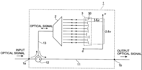
~ To begin with, the schematic of a variable dispersion
compensator is described. FIG. 1 is a block diagram that
illustratively shows the one of the embodiments of a variable
dispersion compensat:or according to the present invention.
Variable dispersion compensator 1 of this embodiment applies
a predetermined amount of phase shift to an input optical
signal to compensate the dispersion of the optical signal,
and is configured comprising optical combining/splitting
unit 2 and reflective mirror group 3. In addition, regarding
the dispersion compensation functionality, the amount of
phase shift that is applied to each frequency component of
the optical signal for dispersion compensation is variable.
An optical signal, which is to become the subject of
dispersion compensation and which has a frequency component
(wavelength component)within a predetermined f requency band
(wavelength band) , is input from input terminal la of variable
dispersion compensator 1, and after a predetermined phase
shift is applied, is output as a dispersion compensated
optical signal from output terminal lb. Between input
terminal la and output terminal lb, there is provided optical
transmission line 11 through which an optical signal is
propagated.
9
CA 02379912 2002-04-02
FPO1-0049-00
Optical circulator 1.2 is provided at a predetermined
position upon optical transmission line 11. In addition,
optical transmission line 13, which is used for dispersion
compensation, is connected to optical circulator 12.
S Through this, the pre-dispersion compensation optical signal
from the input termirial la side of optical transmission line
11 passes through optical circulator 12 to be output towards
optical transmission line 13. In addition, the
post-dispersion compensation optical signal from optical
transmission line 13 passes through optical circulator 12
to be output towards the output terminal lb side of optical
transmission line 11.
The aforementioned optical combining/splitting unit
2 and reflective mirror group 3, in such order, are disposed
at the end of the side opposite optical circulator 12 of
dispersion compensation optical transmission line 13. In
accordance with this optical combining/splitting unit 2 and
this reflective mirror group 3, phase shift is applied to
an optical signal to compensate the dispersion thereof.
Optical combining/ splitting unit 2 is a single optical
combining/splitting means, which functions as an optical
splitting means that inputs the pre-dispersion compensation
optical signal and splits every frequency component of the
optical signal within a predetermined frequency band, and
functions as an optical combining means that combines each
frequency component of the optical signal to give the
CA 02379912 2002-04-02
FPO1-0049-00
post-dispersion compensation optical signal. The optical
signal that is to become the subject of dispersion
compensation, in th.i_s optical combining/splitting unit 2,
is split or combined :by frequency v(or wavelength A ) along
a predetermined splitting direction (direction of the v
-axis in FIG. 1).
In addition, reflect:ive mirror group 3 is a reflecting
means that reflects the respective frequency components of
the optical signal that is split by optical
combining/splitting unit 2 to apply a predetermined phase
shift to each frequency component. Phase shift is applied
to each frequency component of the optical signal using the
optical path length and opt:ical path length differences from
optical combining/ splitting unit2 (optical splitting means)
through reflective mirror group 3 (reflecting means) until
again reaching optical combining/splitting unit 2 (optical
combining means) . In addition, this reflective mirror group
3 is configured to be variable in terms of the reflecting
point for the respective frequency components along the
2C) direction of optical signal propagation (direction of the
d-axis shown in FIG. 1).
Reflective mirror group 3, which is a reflecting means
in this embodiment, comprises a plurality of reflective
mirrors 30, which are divided for every frequency
corresponding to each frequency component of the optical
signal that is split by optical combining/splitting unit
11
CA 02379912 2002-04-02
FP01-0049-00
2. These reflective mirrors 30 are arrayed nearly
continuously having the direction of the v-axis, which is
the direction of the splitting of optical signal and
approximately perpendicular to the direction of optical
signal propagation, as the direction of arrayal; and in
accordance with this, reflective mirror group 3, which
reflects the respective frequency components of the optical
signal within the entire frequencyband that is to be subjected
to dispersion compensation, is formed.
In addition, each respective reflective mirror 30 that
configures reflective mirror group 3 has a fixed shape of
reflective surface; however, each is made as a movable mirror
allowing movement relative to the direction of the d-axis,
which is the direction of optical signal propagation,
separate and independent of each other.
In the above configuration, the optical signal, which
is the subject of dispersion compensation and input to
variable dispersion compensator 1 from input terminal la,
is input to optical combining/splitting unit 2 through
optical transmission line 11, optical circulator 12, and
optical transmission line 13; and each frequency component
is split off according to such frequency V. Each frequency
component of the optical signal that has been split is
propagated towards reflective mirror group 3, and is
reflected at a predetermined reflection position by
corresponding reflective mirror30ofreflective mirror group
12
CA 02379912 2002-04-02
FP01-0049-00
3. Each frequency component that has been reflected is then
combined again by optical combining/splitting unit 2 to
become a post-dispersion compensation optical signal, and
is output to an external portion from output terminal lb
through optical transmission line 13, optical circulator
12, and optical transmission line 11.
Here, the reflection position of a frequency component
of the optical signal for each reflective mirror 30 of
reflective mirror group 3 is determined based on the amount
of phase shift that should be applied to that frequency
component. The drive of each respective reflective mirror
30, which is a movable mirror, is controlled so as to move
it in the direction of optical signal propagation and into
the set reflection position; as a result, dispersion
1`i compensation of the optical signal is achieved within the
entire frequency band.
Next, the optical transmission system comprising the
variable dispersion compensator mentioned above is described.
FIG. 2 is a block diagram that illustratively shows the one
of the embodiments of an optical transmission system
according to the present invention.
The optical transmission system of this embodiment is
configured comprising transmitter (transmitting station)
T, which transmits an optical signal; optical fiber
transmission line L, which is an optical transmission line
that propagates the optical. signal that is transmitted from
13
CA 02379912 2002-04-02
FP01-0049-00
transmitter T; and receiver (receiving station) R, which
receives the optical signal that is propagated through
optical fiber transmission line L.
Variable dispersion compensator 1, which has the
S configuration shown in FIG. 1 is disposed at a predetermined
position upon optical fiber transmission line L. This
variable dispersion compensator 1. is preferably provided
at a position upon optical fiber transmission line L that
is near receiver R, for instance, at a position that is
immediately before receiver R. Through this, dispersion
compensation can be performed for the dispersion that has
accumulated in the optical signal propagating from
transmitter T towards receiver R through optical fiber
transmission line L using variable dispersion compensator
1 before the optical signal is received by receiver R.
In the variable dispersion compensator and optical
transmission system according to this embodiment, where the
optical signal that. is split by the optical splitting means,
optical combining/splitting unit 2, travels until it is
combined again by the optical combining means, optical
combining/splitting unit 2, is used to apply phase shift
to each frequency component of the optical signal. Then as
for reflective mirror group 3, which is the reflecting means
and which is used for setting the optical path length and
phase shift for each frequency component, the reflection
position of the frequency component with respect to
14
CA 02379912 2002-04-02
FP01-0049-00
reflective mirrors 30, which configure reflective mirror
group 3, is made variable by the respective reflective mirrors
30.
Through this, since the phase shift that is applied
'D to each frequency component is variable, it becomes possible
to perform discretionary phase adjustment, and makes it
possible to compensate the dispersion that develops in an
optical signal with high accuracy. Furthermore, since the
separate adjustment of the frequency component reflection
position, with respect to each of the respective reflective
mirrors 30 that configure reflective mirror group 3, is
allowed, the amount of phase shift that is applied to the
optical signal can be controlled with favorable
controllability, thereby making it possible to set or change
the details of the conditions of dispersion compensation.
Moreover, since the control of dispersion compensation
is performed only with the reflecting means, it is possible
to simplify the structure of the optical circuit and allow
for the size reduction of the optical circuit. It is noted
2Cl here that such a reflecting means maybe manufactured using,
for instance, Micro Electro Mechanical System (MEMS)
technology.
With an optical trarismission system that applies a
variable dispersion compensator having such structure,
dispersion that develops in optical signal that propagates
through an optical transmission line such as optical fiber
CA 02379912 2002-04-02
FP01-0049-00
transmission line L may be compensated having favorable
controllability and high accuracv to achieve an optical
transmission system that reliably prevents waveform
deterioration of an optical signal.
It is noted here that with variable dispersion
compensator 1 shown in FIG. 1, single optical
combining/splitting unit 2 is used as optical splitting means
for splitting a pre-dispersion compensation optical signal
into frequency components, and as optical combining means
for combiningfrequency components to give a. post-di spers ion
compensation optical signal. Accordingly, the structure of
variable dispersion compensator 1 is simplified to allow
the further size reduction ofsuch optical circuit. However,
such optical splitt:ing means and optical combining means
may even be configured separately.
FIG. 3 is a planar view showing a more specific
structural example of the variable dispersion compensator
according to this embodiment that is shown in FIG. 1. It
is noted here that in FIG. 3, optical transmission line 11
2C> and optical circulator 12, etc. are not shown, but only the
optical circuit comprising optical combining/ splitting unit
2 and reflective mirror group 3, which actually perform
dispersion compensation of an optical signal, is shown.
In variable dispersion compensator 1 of this example,
arrayed waveguide grating (AWG) 2a with a planar waveguide
type optical circuit that is formed in a predetermined
16
CA 02379912 2002-04-02
FPO1-0049-00
waveguide pattern upon substrate 10 is used as optical
combining/splitting unit 2, which splits and alternately
combines an optical signal that is to become the subject
of dispersion compensation.
AWG 2a is corifigured including input/output channel
waveguide 21, the end thereof being made into an input/output
port; first slab waveguide 22, which is connected to
input/output channel.waveguide 21; array waveguide portion
23, which comprises a plurality of channel waveguides that
are connected to first slab waveguide 22 with each differing
in optical path length from the others; and second slab
waveguide 24, which is connected to array waveguide portion
23.
To the side opposite array waveguide portion 23 of
second slab waveguide 24, there is further connected channel
waveguide group 25, which comprises a plurality of lines
(n lines) of channel waveguides 261 to 26n. In addition,
on the side opposite second slab waveguide 24 of channel
waveguide group 25, there is provided reflective mirror group
3, which comprises n movable reflective mirrors 301r 302,
30õ corresponding to each of the respective n lines of
channel waveguides 261, 262, ..., 26n. These reflectivemirrors
301 to 30, are disposed within trench portion 31, which is
formed across channel waveguide group 25 upon substrate 10,
so as to reflect the respective optical signal components
that are propagated coming through the corresponding channel
17
CA 02379912 2002-04-02
FP01-0049-00
waveguides 261 to 26r,.
More specifically, trench portion 31 is formed along
the direction that is made into the splitting direction of
the optical signal, perperrdicular to direction of optical
signal propagation through channel waveguides 261 to 26, of
channel waveguide group 25 (see FIG.1). Reflective mirrors
301 to 30n of reflective mirror group 3 are then disposed
in positions facing each respective corresponding channel
waveguide 261 to 26n (positions facing the core of the channel
waveguide) in the trench portion 31.
In the above configuration, when an optical signal is
input to input/output channel waveguide 21 from the
input/output port of AWG 2a, the optical signal is split
into every frequency (every wavelength) while being guided
through first slab waveguide 22, array waveguide portion
23, and second slab waveguide 24, in that order. Each
frequency component of the optical signal that has been split
is divided and input to the respective channel waveguides
261 to 26, of channel waveguide group 25.
The respective frequency components that are
propagated through channel waveguides 261 to 26n, are
reflected by corresponding movable reflective mirror 301to
30r, of reflective mirror group 3, and are again propagated
in the opposite direction through respective channel
waveguides 261 to 26,. Each frequency component is then
combined while beirig guided through second slab waveguide
18
CA 02379912 2002-04-02
FPO1-0049-00
24, array waveguide portion 23, and first slab waveguide
22, in that order, outputting the dispersion compensated
optical signal from the input/output port through
input/output channel waveguide 21.
Here, reflect.ive mirror group 3, whichis the reflective
means in this embod:i.ment, is configured by a plurality of
movable reflectivemirrors :30,the reflectivesurface thereof
capable of being moved separately, as described above. As
a method of driving these movable reflective mirrors 30,
it is preferable that the electrostatic force that develops
due to the application of voltage between an electrode (first
electrode) that is provided on movable mirror 30 and an
electrode (second electrode) that is provided at a
predetermined position relative to the first electrode be
used to perform such drive control. Through this, the control
of the reflection position at the reflective mirror, and
the amount of phase shift and conditions of dispersion
compensation set thereby, can be performed easily and at
high speeds.
2C) FIG. 4 is a block diagram showing an example of the
movable reflective mirrors that is used as the reflective
mirror group in the variable dispersion compensator shown
in FIG. 3. This reflective mirror group 3 has a plurality
of movable reflective mirrors 30, which are arrayed within
2S trench portion 31 as described above. In addition,
respective guide rails 32 are provided between neighboring
19
CA 02379912 2002-04-02
FPO1-0049-00
movable reflective mirrors 30 to guide the shift direction
of movable reflective mirrors 30.
Each respective movable reflective mirror 30 is
supported by mirror support section 33, which preferably
comprises an insulating material. Mirror support section
33 is made movable with the end opposite reflective mirrors
30 as a point of support, and electrode 34, which is the
first electrode, formed on one side. In addition, electrode
35, which is the second electrode, is provided on the side
opposite electrode :34, with mirror support section 33 in
between them. This electrode 35 is fixeci relative to
substrate 10.
An adjustable electr_Lc power source, which adjustably
applies voltage, is connected between electrode 34, which
is provided on mirror support section 33, and electrode 35,
which is fixed on substrate 10. If the applied voltage
between this electrode 34 and electrode 35 changes, then
a deflection develops at mirror support section 33 due to
the electrostatic force that develops or the change therein,
and movable reflective mirror 30 moves to this deflection
in order to be shifted in the shift direction that is guided
by guide rail 32.
FIG. 5 is a block diagram showing another example of
a movable reflective mirror. This reflective mirror group
3 is similar to the structural examples in FIG. 4 in regards
to movable reflective mirror 30 being arrayed within trench
CA 02379912 2002-04-02
FP01-0049-00
portion 31, guide rail 32, and mirror support section 33;
however, differs in the structure of the electrodes for
driving reflective mirror 30.
Comb-shaped electrodes 36 are formed on both sides of
mirror support section 33. Opposite these, similar
comb-shaped electrodes 37 and 38 are provided on both sides
of mirror support section 33. By changing the respective
voltage applied to these comb-shaped electrodes 36, 37, and
38, movable reflective mirror 30 is shifted. In such cases
where comb-shaped electrodes are used, reflective mirror
30 is allowed to be effectively driven with favorable
accuracy.
The dispersion that develops in an optical signal in
an optical transmission system, and dispersion compensation
using a variabledispersion compensator arefurther described
while referencing FIG. 1 and FIG. 2. It is noted that in
the following, optical intensity of an optical signal that
is the subject of dispersion compensation is assumed as given
by the value of amplitude JEJ of that electric field, or
the value of the square thereof.
An optical signal that is propagated through optical
fiber transmission line L in an optical transmission system,
as shown in FIG. 2, is generated in transrnitter T so that
optical intensity IEJ has a predetermined signal waveform
A, and transmitted as an input optical signal to the optical
transmission system. This input optical signal has optical
21
CA 02379912 2002-04-02
FPO1-0049-00
signal components that are spread out across a predetermined
optical signal frequency band (wavelength band) with optical
signal frequency v o (optical signal wavelength /l o= c o) as the median
frequency.
When such an optical signal is propagated through
optical fiber transmission line L, the dispersion of optical
fiber transmission line L accumulates in the optical signal.
The propagated optical signal then, as shown by signal
waveform B in FIG. 2, develops waveform deterioration, where
the signal waveform of optical intensity IE' I is distorted
from signal waveform A of the input optical signal.
In variable dispersion compensator 1, phase shift,
which is used to compensate the dispersion of each frequency
component of optical signal, is applied to each frequency
component of an optical signal that is the subject of
dispersion compensation and in which such waveform
deterioration has developed, so as to negate the phase shift
from dispersion that has accumulated in optical fiber
transmission line L in order to compensate the dispersion.
2C) Through this, an optical signal is obtained having signal
waveform C of optical intensity I E"I , which has removed to
the greatest extent possible the effects of dispersion due
to being propagated through optical fiber transmission line
L.
In more detail, in cases where there exists second order
dispersion (dispersion) D(2) and third order dispersion
22
CA 02379912 2002-04-02
FP01-0049-00
(dispersion slope) D(3) in optical fiber transmission line
L, the value of total dispersion D for the optical signal
components of wavelength A (= c/ v) is givenby the following
expression, wherein group delay time is assumed as r and
1l o is the median wavelength of the above-mentioned optical
signal.
D (1l) = dr / dA
= D (2) + D (3) ( A - /L p)
When second order dispersion D (2) is made dominant in
the total dispersion D, the group delay time Z' for the optical
signal component of wavelength A becomes
r (A) = D (2) ('k - '1o),
At this point, phase shift 95 due to dispersion that develops
in each optical signal component of the optical signal that
has propagated through optical fiber transmission line L,
whenthephase shift atmedian frequency v o(medianwavelength
Ao) is given as 0, becomes the following.
-7t'cD (2) ( ( v - vo) / vo) 2
or when the rate of change of phase shift 4) is
d95 /dv = - (27[cD (z) / v('2)
x (v-vo).
In other words, phase shift that has parabolic change with
a center of median frequency v o develops in an optical signal
that propagates through optical fiber transmission line L
due to dispersion D (2) .
Dispersion compensation is performed using variable
23
CA 02379912 2002-04-02
FP01-0049-00
dispersion compensator 1, which is shown in FIG. 1 and FIG.
3, for an optical signal in which such phase shift develops.
Here, as shown in F'IG. 1, the total width of the frequency
band in the entire reflective mirror group 3 that is to become
the frequency band in which dispersion compensation is
performed is given as 2 (5 V, and the dispersion compensation
resolution, which is the respective frequency width of the
plurality of reflective mirrors 30 that are included in
reflective mirror group 3, is given as 0 V.
Furthermore, in regards to each of the respective
reflective mirrors 301 to 30õ included in reflective mirror
group 3, the median frequency of the frequency component
of the optical signal that is reflected by reflective mirror
30i is given as V i, and the phase shift that is applied for
dispersion compensation in each frequency component of the
optical signal is given as T/1.
The reflection position of each frequency component
in accordance with each respective reflective mirror 301 to
30,is set so that phase shift 0 in optical fiber transmission
2C) line L at median frequency V i of reflective mirror 30i is
negated by making the phase shift applied to a frequency
component of the optical signal due to the reflection at
reflective mirror 30;. become t/1 = - 0 ( V 1) .
Once the reflection position for each of the respective
reflective mirrors 30 is set, each movable reflective mirror
is shifted to have the reflection position that is set.
24
CA 02379912 2002-04-02
FPO1-0049-00
Through this, a configuration that is capable of compensating
dispersion in an optical transmission system is realized.
Position d (see FIG. 1) of movable reflective mirror 30i,
which applies phase shift 2 / ! = - 0 ( v i) can be found with the
following expression, wherein the refractive index of the
medium between optical combining/splitting unit 2 and
reflective mirror group 3 is given as n,
d = co ( vi) / 47tn1/l.
Here, as in the aforementioned examples, in the case
where reflective mirror group 3, which is reflecting means,
is configured from a plurality of divided reflective mirrors
30, within the range of each reflective mirror 30, the amount
of phase shift t/1 that is applied to the frequency component
of an optical signal becomes constant. Accordingly, in order
to effectively perfor.m dispersion compensation of an optical
signal, it is preferable that the dispersion compensation
frequency resolution A V of dispersion compensation in
reflective mirror group 3 be set so that phase shift 0 ( v ) ,
which develops in opt_Lcal signal, does not change drastically
within the frequency range A 1/ that corresponds to one
reflective mirror 30. More specifically, it is preferable
that the frequency resolution A V meet the conditions of
the following expression relative to the rate of change d
dv of phase shift 0 .
I A v x(dO / dV) I <- 7L
When second order dispersion D(`) is dominant in the
CA 02379912 2002-04-02
FPO1-0049-00
total dispersion D, the absolute value of the rate of change
I(dO / dV ) I of phase shift 0 is maximized at the frequency
components at the extremities of the frequency band, which
are separatedby frequency V= vo 8 V , namelyby frequency
8 v which is half of the total width 28 V from median
frequency Vo, with that maximized value being
Id~ / dV Imaz:
= 127Cr.D (21 (5 V / Vo21 .
Accordingly, the maximized value of dispersion D~2) that
meets the above preferred conditions of
IDV x(dO / dv) 7r
becomes
I D 12) 1 max
=vo 2/2cA v8v.
For example, in regards to the optical signal that
becomes the subject of dispersion compensation, if that
median frequency is g:iven as V o= 189. 1 THz (median wavelength
given as A o= 1585 nm) , the half-width of the frequency band
as 8 V = 50 GHz, and the frequency resolution as A v= 5
GHz, which is the frequency range for one reflective mirror,
then it follows that the maximum dispersion capable of being
compensated is I D (`')I maX = 240 ps/nm. In addition, with
similar conditions, if the half-width of the frequency band
is given as 6 V = 15 GHz, and the frequency resolution as
A V= 3 GHz, then it follows that the maximum dispersion
capable of being compensated is ID i211 max = 1300 ps/nm.
26
CA 02379912 2002-04-02
FP01-0049-00
It is noted that using the above expressions, the value
of the maximum dispersion capable of being compensated ID
(2) I,,aX becomes larger as the frequency resolution A V becomes
finer. In regards to this frequency resolution A v, it is
preferable that it be set to a favorable value in consideration
of structure of the variable dispersion compensator, for
example, the splitting conditions of the optical signal due
to AWG 2a in variable dispersion compensator 1, which is
shown in FIG. 3, and the width with which the divided movable
reflective mirrors upon substrate 10 are capable of being
formed.
Here, a more specific structural example of variable
dispersion compensator 1 that is shown in FIG. 3 including
AWG 2a is illustrated. If the interval between neighboring
channel waveguides of channel waveguide group 25 that are
connected to second slab waveguide 24 is given as Ax, and
the wavelength interval between the frequency components
of the optical signal propagated through neighboring channel
waveguides as 0 A , then the following expression is obtained.
2o Ox / A A
= N,fAL / nsAxAo,
wherein N, is the group refractive index of the waveguide,
f is the length of the slab waveguides along their length,
AL is the optical path length difference of the channel
waveguides in the array waveguide portion, and ns is the
effective refractive index of the s]_ab waveguides. Of these
27
CA 02379912 2002-04-02
FP01-0049-00
the group refractive index N, and effective refractive index
ns are in the range of 1.5, respectively.
In this regard, if the median wavelength of the optical
signal is given as A o= 1550 nm and the frequency band in
which dispersion compensation is performed is 28 v= 100
GHz (which correlates to wavelength band Cl . 8 nm) , then the
frequency resolution of this frequency band being divided
into 10 parts becomes A 1/ = 10 GHz. Accordingly, the
wavelength resolution is = 0.08 nm. Furthermore, the
interval between channel waveguides becomes Ax= 20 /im.
If these numeric values are substituted, then as a
structural condition that should be met for AWG 2a of variable
dispersion compensator 1, it is found that
f A L = 7.75 X 10⁻⁶ m.
It is possible to nieet this condition if with a structure,
for example, where the slab waveguide is set with f 30
mm, and the array waveguide portion is set with AL= 258
gm.
It is noted that it is preferable that dispersion
compensation frequency band 28 v be set so that it
sufficiently includes a frequency range throughout which
the optical signal component of the optical signal that is
to become the subject of dispersion compensation is
distributed.
Furthermore, if the optical signal that is to become
the subject of dispersion compensationisanlulti-wavelength
28
CA 02379912 2002-04-02
FP01-0049-00
optical signal comprising a plurality of optical signals
having opticalsignalwavelengthsdifferingfrom each other,
then in cases where dispersion compensation is performed
for a single opticalsignal included in the multi-wavelength
optical signal, it is possible for the frequency interval
between neighboring optical signals to be total frequency
width 26 V. Furthermore, when the total frequency width
2(5 V is made larger than the frequency interval between
neighboring optical signals (e.g. in integral multiples),
1c) the structure becomes capable of dispersion compensating
the plurality of optical signals included a multi-wavelength
optical signal.
Furthermore, in regards to the bit rate (modulation
rate) of the optical signal, it is preferable that the bit
1S rate be 10 Gbps or faster, and even more preferably, 40 Gbps
or faster. The developmerit of dispersion in the optical
transmission line becomesparticula.rly problematic with such
high-speedbit rates; however, even in such cases, by adopting
the configuration described above in a variable dispersion
20 compensator, favorable dispersion compensation of the
optical signal can be performed with sufficient accuracy.
However, needless to say, variable dispersion compensator
1 may be effective:Ly adopted for optical signals with bit
rates that are lower than those mentioned above.
2`i Furthermore, i_t is preferable that the array of the
reflective mirrors that comprise the reflecting means or
29
CA 02379912 2002-04-02
FP01-0049-00
the shape of the reflecting surface be somewhat parabolic
in relation to the frequency component to be reflected.
Through this, in cases where second order dispersion D1Z)
becomes dominant in the dispersion that develops in the
'D optical transmission line, it is possible to achieve
favorable dispersion compensation for an optical signal
throughout the entire f requency band that becomes the subj ect
of dispersion compensation.
Simulations were performed by applying the specific
conditions in the optical transmission system and variable
dispersion compensator having the configuration mentioned
above, and the results were confirmed with regard to
dispersion compensation of the optical signal and waveform
deterioration of the optical signal due to dispersion in
the optical transmission line.
As for the optical signal that was to become the subject
of dispersion compensation, the median frequency was set
at v o= 189 . 1 THz (median wavelength of /lo= 1585 nm), in
addition, the modulation scheme was set to NRZ, andmodulation
rate (bit rate ) M set to either 10 Gbps or 40 Gbps. In addition,
the waveform of the optical. pulse of the optical signal was
set to be a super-Gaussian, non-chirp form. Here, if the
duration of the one-bit signal is given as 2to ( = 1 / M),
then the signal waveform of the optical signal is applied
as
E ( t ) _exp { -log2 / 2
CA 02379912 2002-04-02
FP01-0049-00
X (t / t0) 2mt r
whereinm is given as the parameter that determines the optical
pulse form and here it is set to m = 2.
Furthermore, random codes of 29 = 512 bits were
transmitted as the optical signal to actually be subjected
to dispersion compensation, and the obtained signal waveform
was estimated through the eye pattern displayed.
To begin with, an example of dispersion compensation
in the case where the bit rate was made to be M = 10 Gbps
is illustrated. With this 10 Gbps bit rate, the clock for
the signal period is 100 ps.
FIG. 6A and 6B are graphs illustrating an example of
the optical signal that the 10 Gbps optical transmission
system transmits, wherein FIG. 6A illustrates the signal
waveform of the input optical signal immediately after the
transmitter (refer to signal waveform A in FIG. 2) ; and FIG.
6B illustrates the signal waveform of the output optical
signal before dispersion compensation (without dispersion
compensation) (refer to signal waveform B in FIG. 2).
The input optical signal having the signal waveform
shown in FIG. 6A has frequency components in a frequency
range of approximately 15 GHz, with optical signal
frequency 1/ o = 189. 1'THz as the median. In this regard, when
the dispersion that develops in the optical signal due to
propagation in the optical transmission line is set as D
(2) = +1200 ps/nm, 17 (3) = 0 ps/nm`, the signal waveform in
31
CA 02379912 2002-04-02
FP01-0049-00
the post-propagation output optical signal becomes a waveform
with developed waveform deterioration due to dispersion,
as shown in FIG. 6B.
FIG. 7A and 7B are graphs showing an example of
.3 dispersion compensation for an optical signal that is
transmitted by a10Gbpsopticaltransmissionsystem,wherein
FIG. 7A illustrates the phase shift of the optical signal,
and in addition, FIG. 7B illustrates the waveform of the
output optical signal after dispersion compensation (with
dispersion compensation) (refer to signal waveform C in FIG.
2).
Here, in FIG. 7A, the horizontal axis shows the relative
frequency V - V o(GHz) vis-a-vis median frequency V o= 189. 1
THz. In addition, the vertical axis shows the rate of change
of phase shift dO /dv (rad/GHz) corresponding to dispersion
D(z) = +1200 ps/nm and phase shifts 0 and -t/1 (rad) .
For each frequency component of the input optical signal
shown in FIG. 6A, due to dispersion Din the above-mentioned
optical transmission line, the parabolic phase shift 0 shown
in FIG. 7A develops in the post-propagation output optical
signal shown in FIG. 6B. In this regard, in this example,
dispersion compensation is performed with the half-width
of frequency band being set to 8 V = 15 GHz, and frequency
resolution set to A V = 3 GHz.
At this point, in variable dispersion compensator 1,
phase shift tP, which is shown as the graph of -V) in FIG.
32
CA 02379912 2002-04-02
FPO1-0049-00
7A, is applied to each frequency component of the optical
signal. This graph of phase shift t/i with a stepped-shape
at frequency width A V = 3 GHz corresponds to the array of
the plurality of reflective mirrors 30 in reflective mirror
~ group 3. In other words, the direction of the horizontal
axis of phase shift t/1 corresponds to the position of
reflective mirror 30 along the V-axis. In addition, the
direction of the vertical axis corresponds to the position
of reflective mirror 30 along the d-axis (refer to FIG. 1) .
Reflective mirror group 3, as shown in FIG. 7A, is
configured so that the two phase shifts match with -t/1 =0
( V i) at the respective median frequency V i for the frequency
component of frequency width A V reflected by each
reflective mirror 30i . With such configuration, phase shift
0, which develops in the optical signal along the optical
transmission line, is negated to the greatest extent possible
by phase shift t/1, which is applied by variable dispersion
compensator 1. As shown in FIG. 7B by the signal waveform
of the post-dispersion compensation output optical signal,
dispersion in the opti.calsignalissufficiently compensated.
FIG. 8A and 8B are graphs of another example of
dispersion compensation of an optical signal propagated by
a 10 Gbps optical transmission system, wherein FIG. 8A shows
the phase shift of the optical signal, and in addition, FIG.
8B shows the signal waveform of the post-dispersion
compensation output optical signal. It is noted that in the
33
CA 02379912 2002-04-02
FPO1-0049-00
graph of FIG. 8A, the rate of change of phase shift do/d
v and phase shift 0 are the same as that shown in FIG. 7A.
For each frequency component of the input optical signal
shown in FIG. 6A, due to dispersion D(2) in the above-mentioned
'D optical transmission line, the parabolic phaseshift 4) shown
in FIG. 8A develops:in the post-propagation output optical
signal shown in FIG. 6B. In this regard, in this example,
dispersion compensation is performed with the half-width
of frequency band being set to (5 v = 15 GHz, and frequency
resolution set to A v= 1 GHz.
At this point, in variable dispersion compensator 1,
phase shift 7/1, which is shown as the graph of -0 in FIG.
8A, is applied to each frequency component of the optical
signal. This graph of phase shift tP with a stepped-shape
at frequency width L1 v= 1 GHz corresponds to the array of
the plurality of reflective mirrors 30 in reflective mirror
group 3.
Reflective mirror group 3, as shown in FIG. 8A, is
configured so that the two phase shifts match with -t/J =0
( v i) at the respective median frequency v i for the frequency
component of frequency width 0 V reflected by each
reflective mirror 30i. With such configuration, phase shift
0, which develops in the optical signal along the optical
transmission line, is negated to the greatest extent possible
by phase shift V), which is applied by variable dispersion
compensator 1. As shown in FIG. 8B by the signal waveform
34
CA 02379912 2002-04-02
FP01-0049-00
of the post-dispersion compensation output optical signal,
dispersion in the optical signal is suf f iciently compensated.
In particular, in this example, by making the frequency
resolution A V 1 GHz, which is smaller than the 3 GHz of
~ the example shown in E'IG. 7A and 7B, the accuracy of dispersion
compensation is improved.
Next, an example of di_spersion compensation in the case
where the bit rate is made to be M= 40 Gbps is shown. With
this 40 Gbps bit rate, the clock that is to become the period
of the signal is 25 ps.
FIG. 9A and 9B are graphs illustrating an example of
the optical signal that the 40 Gbps optical transmission
system transmits, wherein FIG. 9A illustrates the signal
waveform of the input optical signal immediately after the
transmitter; and FIG. 9B illustrates the signal waveform
of the output optical signal before dispersion compensation.
The input optical signal having the signal waveform
shown in FIG. 9A has frequency components in a frequency
range of approximately 50 GHz, withoptical signal frequency
Vo = 189.1 THz as the median. In this regard, when the
dispersion that develops in the optical signal due to
propagation in the optical transmission line is set as D
(2) = +200 ps/nm, D(3) = 0 ps/nm`, the signal waveform in the
post-propagation out:put optical signal becomes a waveform
with developed waveform deterioration due to dispersion,
as shown in FIG. 9B.
CA 02379912 2002-04-02
FP01-0049-00
FIG. 10A and 1.0B are graphs showing an example of
dispersion compensation for an optical signal that is
transmitted by a 4 0 Gbps optical transmission system, wherein
FIG. 10A illustrates the phase shift of the optical signal,
ED and in addition, FIG. lOB illustrates the waveform of the
output optical signal after dispersion compensation.
Here, in FIG. 10A, the horizontal axis shows the
relative frequency v- 1/ o(GHz) vis-a-vis median frequency
vo = 189.1 THz. In addition, the vertical axis shows the
rate of change of phase shift d0 /dv (rad/GHz) corresponding
to dispersion D(') = +200 ps/nm and phase shifts 0 and -
(rad).
For each frequency component of the input optical signal
shown in FIG. 9A, due to dispersion Din the above-mentioned
optical transmission line, the parabolic phase shift 0 shown
in FIG. 10A develops in the post-propagation output optical
signal shown in FIG. 9B. In this regard, in this example,
dispersion compensation is performed with the half-width
of frequency band being set to 8 1/ = 50 GHz, and frequency
resolution set to AV = 2 GHz.
At this point, in variable dispersion compensator 1,
phase shift 2/i, which is shown as the graph of -V) in FIG.
10A, is applied to each frequency component of the optical
signal. This graph.of phase shift t/i with a stepped-shape
at frequency width A V = 2 GHz corresponds to the array of
the plurality of reflective mirrors 30 in reflective mirror
36
CA 02379912 2002-04-02
FP01-0049-00
group 3.
Reflective mirror group 3, as shown in FIG. 10A, is
configured so that the two phase shifts -i// =0 ( V i) match
at the respective median frequency vL for the frequency
component of frequency width A v reflected by each
reflective mirror 30i. With such configuration, phaseshift
0, which develops in the optical signal along the optical
transmission line, is negated to the greatest extent possible
by phase shift t/i, which is applied by variable dispersion
compensator 1. As shown iri FIG. lOB by the signal waveform
of the post-dispersion compensation output optical signal,
dispersion in the opti.calsignalissufficiently compensated.
In the above-mentioned embodiment, as shown in Fig.
l and Fig. 3, reflective mirror group 3, comprising a plurality
1_`) of movable reflective mirrors 30, is utilized as reflecting
means. Contrarily, it. is also possible to use a single movable
reflective mirror, which is not divided into a plurality
of reflective mirrors, as reflecting means.
FIG. 11A and F'IG. 11B are diagrams illustrating a
movable reflective mirror when using a single movable
reflective mirror asreflecting meansin variable dispersion
compensation, wherei.n FIG. 11A is a schematic showing the
shape and driving method thereof, and FIG. 11B is a block
diagram showing a more specific example.
Reflecting means 4 shown in FIG. 11A and FIG. 11B
comprises single movable reflective mirror 40. By making
37
CA 02379912 2002-04-02
FPO1-0049-00
the entire reflective surface of this movable reflective
mirror 40 into a shape having a curved surface (for example,
making it into a shape having a parabolic-shape) as shown
inFIG. 11A, it is possible to shift the respective reflective
surface portion corresponding to each frequency component
of the optical signal in the direction of optical signal
propagation. Through this, variable dispersion
compensation can be performed with favorable accuracy in
the same manner as reflective mirror group 3, which comprises
a plurality of divided movable reflective mirrors 30.
The structural example shown in FIG. 11B, for example,
may be used as a more specific structure of reflecting means
4 having such single movable reflective mirror 40. With this
reflecting means 4, a metal layer 40, which becomes a movable
reflective mirror, is formed upon polysilicon layer 41. In
addition, this metal layer 40 functions as a first electrode
provided on the movable reflective mirror.
Onthe side opposite metal layer 40 of polysilicon layer
41, there is disposed metal layer 43, which is formed upon
silicon layer 44. This metal layer 43 becomes the second
electrode provided at a predetermined position relative to
the first electrode. In addition, polysilicon layer 41 and
metal layer 43 are separated by silicon oxide layer 42. This
silicon oxide layer 42 is provided at the ends of polysilicon
2E. layer 41 and metal layer 43.
Between metal layer 40, which functions as a movable
38
CA 02379912 2002-04-02
FP01-0049-00
reflective mirror together with being the first electrode,
and metal layer 43, which is the second electrode, there
is connected a variable power source, which adjustably
applies a voltage. When the applied voltage between this
metal layer 40 and metal layer 43 changes, a deflection due
to the generated electrostatic force, or the change thereof,
develops in the middle of metal layer 40 and polysilicon
layer 41 where silicon oxide layer 42 is not provided to
change the curved shape of the reflective surface and
therefore shift therespect.ive reflection surface portions.
In cases where an.AWG is utilized similar to optical
combining/splitting unit 2 of the embodiment shown in FIG.
3, it is preferable that reflecting means 4 with such
configuration be disposed along the output.terminal of the
second slab waveguide.
FIG. 12 is a block diagram that illustratively shows
another embodiment of a variable dispersion compensator when
using the single reflective mirror as reflective means.
Variabledispersion compensatorlofthisembodiment,similar
2C, to the variable dispersion compensator illustrated in FIG.
1, applies a predetermined amount of phase shift to an input
optical signal to cornpensate the dispersion of the optical
signal, and is configured comprising optical
combining/splitting unit 2 and reflective means 4. In
addition, regarding the dispersion compensation
functionality, the amount of phase shift that is applied
39
CA 02379912 2002-04-02
FP01-0049-00
to each frequency component of the optical signal for
dispersion compensation is variable.
In variable dispersion compensator 1 shown in FIG.
12, optical transmission line 11, optical circulator 12 and
optical transmission line 13 for dispersion compensation
have the same structure as those of the variable dispersion
compensator illustrated in Fig. 1.
The aforementioned optical combining/splitting unit
2 and reflective means 4 are disposed in this order at the
end of the side opposite cptical circulator 12 of optical
transmission line 13 for dispersion compensation. This
opticalcombining/splittin.g unit 2 and this reflective means
4 apply a phase shift to an optical signal, whereby the
dispersion thereof is compensated.
Opticalcombining/splitting unit 2 is a single optical
combining/splitting means, which functioris as an optical
splitting means that inputs the pre-dispersion compensation
optical signal and demultiplexes every frequency component
of the optical signal within a predetermined frequency band,
and functions as ari optical combining means that combines
each frequency component of the optical signal to give the
post-dispersion compensation optical signal. The optical
signal that is to become the subject of dispersion
compensation, in this optical combining/splitting unit 2,
is split or combined by frequency 7/ (or wavelength A ) along
a predetermined splitting direction (direction of the V
CA 02379912 2002-04-02
FPO1-0049-00
-axis in FIG. 12).
In addition, reflective means 4 is a reflecting means
that reflects the respective frequency components of the
optical signal that is split by optical combining/splitting
unit 2 to apply a predetermined phase shift to each frequency
component. Phase shift is applied to each frequency
component of the optical signal using the optical path length
and optical path length differences from optical
combining/splitting unit 2 (optical splitting means) through
reflective means 4 until again reaching optical
combining/splitting unit 2 (optical combining means). In
addition, this reflectivemeans 4 is configuredtobe variable
in terms of the reflecting point for the respective frequency
components along the direction of optical signal propagation
(direction of the d-axis shown in FIG.12).
Reflective means 4, which is a reflecting means in this
embodiment, is structured from a single reflective mirror
40. This single reflective mirror 40 is disposed in the
direction of the v-axis, which is the direction of the
splitting of optical signal and approximately perpendicular
to the direction of optical signal propagation, as the
direction of spread of reflective surface; and in accordance
with this, reflective means 4, which reflects the respective
frequency components of the optical signal within the entire
frequency band that is to be subjected to dispersion
compensation, is formed. The structure and driving method
41
CA 02379912 2002-04-02
FP01-0049-00
of reflective mirroi- 40 is as per the description of FIG.
11A.
In the above configuration, the optical signal, which
is the subject of dispersion compensation and input to
`i variable dispersion comperisator 1 from input terminal la,
is input to optical combining/splitting unit 2 through
optical transmission line 11, optical circulator 12, and
optical transmission line 13, and is split off into frequency
components by the frequency v thereof. Each frequency
component of the optical signal that has been split is
propagated towards reflective means 4, and is reflected at
a predetermined reflection position by corresponding
reflective surface portion of reflective mirror 40. Each
frequency component that has been reflected is then combined
again by optical combining/splitting unit 2 to become a
post-dispersion compensation optical signal, and is output
to an external portiori from output terminal lb through optical
transmission line 13, optical circulator 12, and optical
transmission line 11.
Here, the reflection position of a frequency component
of the optical signal for each reflective surface of
reflective mirror 40 of reflective means 4 is determined
based on the amount of phase shift that should be applied
to that frequency componerit. The deformation of the
reflective surface of reflectivemirror 40, which is amovable
mirror, is controlled so as to move the respective reflective
42
CA 02379912 2002-04-02
FPO1-0049-00
surfaces in the direction of optical signal propagation and
into the set reflection position; as a result, dispersion
compensation of the optical signal is achieved within the
entire frequency band.
With the variable dispersion compensator according to
the present embodiment, similar to the variable dispersion
compensator of the embodiment illustrated in Fig. 1,
arbitrary phase adjustment is possible since the phase shift
provided to the respective frequency components of the
optical signal becomes variable, and the dispersion generated
in the optical signal can be compensated with high precision.
Moreover, by applying this variable dispersion compensator
in an optical transmission system, the dispersion generated
in the optical signal propagated through the optical
transmission line can be compensated with high precision
and favorable controllability, and realized thereby is an
optical transmission system capable of reliably preventing
waveform deterioration or the like of optical signals.
FIG. 13 is a plan view showing a concrete structural
example of the variable dispersion compensator according
to the embodiment illustrated in FIG. 12. Similar to FIG.
3, it is noted here that in FIG. 13, optical transmission
line 11 and optical circulator 12, etc. are not shown, but
only the optical circuit comprising optical
combining/splitting unit 2 and reflective means 4, which
actually perform dispersion compensation ofan optical signal,
43
CA 02379912 2002-04-02
FPO1-0049-00
is shown.
In variable dispersion compensator 1 of this example,
Arrayed Waveguide Grating (AWG) 2b with a planar waveguide
type optical circuit that is formed in a predetermined
waveguide pattern upon substrate 10 is used as optical
combining/splitting unit 2, which splits and alternately
combines an optical signal that is to become the subject
of dispersion compensation.
AWG 2b is configured including input/output channel
1Cl waveguide 21, the end thereof being made into an input/output
port; first slab waveguide 22, which is connected to
input/output channel waveguide 21; array waveguide portion
23, which comprises a plurality of channel waveguides that
are connected to first slab waveguide 22 with each differing
in optical path length from the others; and second slab
waveguide 24, which is connected to array waveguide portion
23. Moreover, movable reflective mirror 40, which is
reflective means 4, is provided to the side opposite array
waveguide portion :23 of second slab waveguide 24.
Here, with variable dispersion compensator 1
illustrated in FIG. 1.3, shown is a structural example where
n number of movable reflective mirrors 40, to 40r, is provided
as reflective means 4. Each of these movable mirrors 401 to
40n corresponds to reflective mirror 40 illustrated in FIG.
11A and FIG. 12, respectively. In other words, in this
structural example, the frequency band of the optical signal,
44
CA 02379912 2002-04-02
FPO1-0049-00
which is the subject of dispersion compensation, is divided
into n number of bands, and, dispersion compensation is
performed within the respective frequency bands by providing
a single movable reflective mirror 40 illustrated in FIG.
12 for each n number of frequency bands divided as described
above.
Each of movable mirrors 401 to 40n structuring
reflective means 4:is a movable mirror capable of moving
each of the reflective surfaces corresponding to each
frequency component in the optical signal propagation
direction by deforming its entire reflective surface. The
deformation method of the reflective surface is as per the
description of reflective mirror 40 illustrated in FIG. 11A
and FIG. 12.
1`i In the above configuration, when an optical signal is
input to input/output channel waveguide 21 from the
input/output port of AWG 2b, the optical signal is split
into every frequency (every wavelength) while being guided
through first slab waveguide 22, array waveguide portion
23, and second slab waveguide 24, in that order.
Each frequency component of the optical signal that
has been split is reflected with corresponding movable
reflective mirrors 40i to 40, of reflective means 4 per
frequency band divided into n numbers. Each frequency
component is then combined while being guided through second
slab waveguide 24, array waveguide portion 23, and first
CA 02379912 2002-04-02
FPO1-0049-00
slab waveguide 22, in that order, outputtirig the dispersion
compensated optical signal from the input/output port through
input/output channel waveguide 21.
Further, the reflective means structured from n number
`i of reflective mirrors illustrated in FIG. 13, for example,
may be used in cases when n channels of optical signals each
having a different wavelength are the subject of dispersion
compensation. Here, dispersion compensation is performed
by reflecting the optical signal with a movable reflective
mirror corresponding to each of the n channels of optical
signals.
Generally, it is preferable to set the number of movable
reflective mirrors in accordance with the number of channels
of optical signals subject to dispersion compensation or
the broadness of the frequency band of the optical signal.
For example, when the optical signal is 1 channel, or when
the frequency band is relatively narrow in a plurality of
channels, the structure may be such that n=1 as shown in
FIG. 12 and to provide one movable reflective mirror 40 for
the entire exit of second slab waveguide 24.
FIG.14Aisa diagram showing another structural example
of the movable reflective mirror in the case of using a single
reflective mirror. With this reflective means 4, similar
to the reflective means illustrated in FIG. 11A and FIG.
11B, a single movable reflective mirror 40 is used, and the
structure is such that each of the reflective surfaces thereof
46
CA 02379912 2002-04-02
FP01-0049-00
may be moved in the optical signal propagation direction
by deforming the entire reflective surface thereof into a
curved surface shape.
With movable reflective mirror 40 of reflective means
illustrated in FIG. 14A, portions 401 and 402 in the vicinity
of the end portions on both sides thereof are provided as
fixed portions, and the portion 403 in the vicinity of the
center thereof is provided as a drive portion capable of
being driven in the optical signal propagation direction
1() with driving means. And, comb drive 45, which is driving
means for driving drive portion 403 in the optical signal
propagation direction, is connected to this drive portion
403.
Comb drive 45 in this embodiment comprises a structure
1`i of combining a comb-shaped electrode in 7 sections. Seven
sections of comb-shaped electrodes 461 to 467 are provided,
with respect to frame shape electrode 460 having a width
wO in the drive direction, to drive electrode 46 for driving
movable reflective mirror 40 in the optical signal
20 propagation direction. This drive electrode 4 6 is established
with the drive direction as a direction approximately
perpendicular to movable reflective mirro:r 40, which is a
propagation direction of the optical signal reflected with
movable reflective mirror 40, and connected to drive portion
25 403 of movable reflective mirror 40 via connection portion
468.
47
CA 02379912 2002-04-02
FPO1-0049-00
Seven sections of comb-shaped electrodes 471 to 477
are provided so as to mutually engage with corresponding
comb-shaped electrode portions 461 to 467, respectively,
with respect to the comb-shaped electrode portions 461 to
467 of these drive electrodes 46. These comb-shaped
electrodes 471 to 477 are fixed to a substrate or the like
to which is provided movable reflective mirror 40 and the
respective electrodes, and, for example, are electrically
connected to each other so as to have the same potential.
In comb drive 45 having the foregoing electrode
structure, by applyirig power voltage between drive electrode
46 including comb-shaped electrode portions 461 to 467 and
comb-shaped electrodes 471 to 477, drive electrode 46 moves
in the drive direction, which is the optical signal
propagation direction, pursuant to static electricity with
respect to the fixed comb-shaped electrodes 471 to 477. Here,
drive portion 403 in the vicinity of the center of movable
reflective mirror 40 connected to drive electrode 46 via
connection portion 468 is driven in the optical signal
propagation direction, and the entire reflective surface
thereof becomes deformed.
As described above, according to the structure of
driving and deforming the portion in the vicinity of the
center of movable reflective mirror 40, as a result of
deforming the entire reflective surf ace of reflective mirror
40 by making if link with the deformation of drive portion
48
CA 02379912 2002-04-02
FP01-0049-00
403 in the center, each of such reflective surfaces can be
effectively moved in the optical signal propagation
direction.
Moreover, when making the portion 403 in the vicinity
of the center of movable reflectivemirror 40 the driveportion,
it is necessary to fix a prescribed portion other than drive
portion 403. With respect to this portion to be fixed, for
example, as illustrated in. the structural example of FIG.
14A, it is preferable that portions 401, 402 in the vicinity
of the end portions on both. sides are provided as the fixed
portions. Or, portions other than in the vicinity of the
end portions, for example, portions between the center and
end portion may be fixed.
An example of a concrete structure of comb drive 45
shown in FIG. 14A is explained with reference to the partially
enlarged view of comb-shaped electrode portion 461 of drive
electrode 46 and corresponding comb-shaped electrode 471
illustrated in FIG. 14B. Foremost, as the overall drive
electrode 46, width in the longitudinal of frame-shaped
electrode portion 460 was set to w0=610um, and structured
as a 7-section electrode as depicted in E'IG. 14A.
Further, regarding the structure and the like of the
respective comb-shaped electrodes, the width of the
comb-shaped electrode was set to w2=10}lm, the gap in the
drive direction between the comb-shapedelectrodesin a state
where drive electrode 46 is in its initial position was set
49
CA 02379912 2002-04-02
FP01-0049-00
to g1=601im, the gap between the combs in the direction
perpendicular to the drive direction was set to g2=10}im,
the length of the overlapping portion of the comb-shaped
electrodes was set to t=l0 m, the height of the respective
electrodes was set to 50urn, and the number of comb-shaped
electrodes is set to 19. As for movable reflective mirror
40, the distance from drive portion 403 in the center to
fixed portion 401 or 402 at the end was set to 1001im, and
the thickness was set to 2.5um.
In comb drive 45 having the foregoing structure, upon
applying a 100V power voltage between drive electrode 46
and comb-shaped electrodes 471 to 477, the displacement of
drive electrode 46 and drive portion 403 of movable reflective
mirror 40 connected to drive electrode 46 was 0.2um. Movable
reflective mirror 40 develops a deflection pursuant to the
displacement of this drive portion 403, and the entire
reflective surface deforms as a result thereof.
FIG. 15 is a diagram showing another structure example
of a movable reflective mirror in a case of using a single
reflective mirror. With this reflective means 4, similar
to the reflective means illustrated in FIG. 11A, a single
reflective mirror 40 is used, and the structure is such that
each of the reflective surfaces moves in the optical signal
propagation direction by deforming the entire reflective
surface into a curved surface shape.
Movable reflective mirror 40 of reflective means 4
CA 02379912 2002-04-02
FPO1-0049-00
illustrated in FIG. 15 has portions 401, 402 in the vicinity
of the endportions onboth sides thereof as the fixedportions.
And, as illustratively shown in FIG. 15, heating means 50
for heating movable reflective mirror 40 is provided to a
prescribed portion (partially or entirely) of movable
reflective mirror 40.
In the aforementioned structure, when a part or the
whole of the portion of movable reflective mirror 40 is heated
with heating means 50, movable reflective mirror 40 deforms
pursuant to thermal expansion or the like, and the entire
reflective surface deforms as a result thereof.
As described above, by making the structure such that
movable reflective mirror 40 is heated and deformed, it
becomes possible to deform the reflective surface of amovable
mirror with a heating means, and it is thereby possible to
simplify the structure thereof and the miniaturize the
dispersion compensator. For example, upon applying heat of
Ot=300 C to an Si beam having a thickness of 2.5pm, 4um of
displacement was obtained at the portion in the vicinity
of the center of movable reflective mirror 40.
Here, when employing the structure of fixing the portion
in the vicinity of the end portions on both sides of movable
reflective mirror 40 and deforming the reflective surface,
in comparison to the structure of fixing the portion in the
vicinity of the center of movable reflective mirror 40 and
deforming the reflective surface, force to be applied to
51
CA 02379912 2002-04-02
FPO1-0049-00
reflective mirror 40 is smaller in the structure of fixing
the portion in the vicinity of the center and driving the
portion in the viciriity of the end portion.
In other words, as shown in FIG. 16A and FIG. 16B, when
S comparing the case of fixingportions 401, 402 in the vicinity
of end portions on both sides thereof with the case of fixing
portion 403 in the vicinity of the center with respect to
movable reflective mirror 40 having the same shape, with
the structure of fixing portions 401, 402 in the vicinity
of the end portions (FIG. 16A), force of f0=8.7X10⁴uN was
required in order to displace the portion in the vicinity
of the center 5um.
Contrarily, with the structure of fixing portion 403
in the vicinity of the center (FIG. 16B) , when applying force
of f1=f2=f0/2=4.35X104uN, respectively, to the portion in
the vicinity of the erid portion so as to make the total force
equal the aforementioned example, the displacement of the
portion in the vicinity of the end portion approximately
quadrupledto19.6um.Moreover, when making the displacement
of movable reflective mirror 40 similar to the above at 5pm,
the total force to be applied to the portion in the vicinity
of the end portion became approximately 1/4 the force at
approximately 2 X 1C)4taN.
As described above, by employing the structure of
driving the portion in the vicinity of the end portion of
the movable mirror, the force necessary to be applied for
52
CA 02379912 2002-04-02
FP01-0049-00
driving the movable mirror becomes small, and the entire
reflective surface thereof can easily be deformed.
Moreover, as the structure of deforming the reflective
surface by fixing the portion in the vicinity of the end
portion on both sides of movable reflective mirror 40, in
addition to the structure of completely fixing portions 401,
402 in the vicinity of the end portion shown in FIG. 16A,
the structure shown in FIG. 16C may also be employed. With
the structure shown in FIG. 16C, portions 401, 402 in the
vicinity of the end portion on both sides are fixed with
respect to the application.direction of force f3 to be the
drive direction of movable reflective mirror 40, but can
move in the longitudinal direction of movable mirror 40
perpendicular to the drive direction.
With the structure shown in FIG. 16C, when the
displacement of movable reflective mirror 40 is made the
same, the force f3 to be added will become approximately
1/4 the force of force fO of FIG. 16A. Therefore, according
to this type of structure, the force necessary to be applied
for driving the movable mirror will become small, thereby
making the deformation of the entire reflective surface
easier.
FIG. 17 is a diagram showing a structural example upon
fixing the portion in the vicinity of the center thereof
with respect to the movable reflective mirror when using
asingle ref lective mirror. This ref lective means 4 comprises
53
CA 02379912 2002-04-02
FPO1-0049-00
single movable reflective mirror40, comb drive 55 including
drive electrode 56 structured of frame-shaped electrode
portion 560 and comb-shaped electrode portions 561 to 567,
and comb-shaped electrodes 571 to 577, and has a structure
similar to the reflective means shown in FIG. 14A regarding
the example of fixing the portion in the vicinity of the
end portion.
With movable reflective mirror 40 of reflective means
4 shown in FIG. 17, portion 403 in the vicinity of the center
thereof is made the fixed portion, and portions 401, 402
in the vicinity of the end portion on both sides are provided
as the drive portions capable of being driven in the optical
signal propagation direction with a drive means. And, the
aforementioned comb drive 55, which is the drive means for
driving drive portions 401, 402 in the optical signal
propagation direction, is connected to such drive portions
401, 402 via connection portions 568, 569, respectively.
In the foregoing structure, when applying a power
voltage between drive electrode 56 including comb-shaped
electrode portions 561 to 567 and comb-shaped electrodes
571 to 577, drive electrode 56 moves in the drive direction,
which is the optical signal propagation direction, pursuant
to static electricity with respect to the fixed comb-shaped
electrodes 571 to 577. Here, drive portions 401, 402 in the
vicinity of the center of movable reflective mirror 40
connected to drive electrode 56 via connection portions 568,
54
CA 02379912 2002-04-02
FPO1-0049-00
569 are driven in the optical signal propagation direction,
and the entire reflective surface thereof becomes deformed.
By employing the structure of driving drive portions 401,
402 in the vicinity of the end portion of movable reflective
S mirror 40 as described above, it becomes pcssible to deform
the reflective surface with relatively small force.
The variable dispersion compensator according to the
present invention and the optical transmission system
comprising the same are not limited to the embodiments
described above, and may be modified in various forms. For
example, the optical combining/splitting unit, which
performs splitting and combining of the optical signal is
not limited to an AWG, but various elements may also be used,
or alternatively, the optical splitting unit and optical
combining unitmay also be providedseparately. Furthermore,
in regards to the splitting of the optical signal, splitting
may be performed so as to divide into a plurality of frequency
components, for example, according to the configuration of
the reflecting means, or alternatively, splitting may also
be performed into a continuous spectral shape by frequency.
FIG. 18 is a block diagram that illustratively shows
another embodiment of the variable dispersion compensator.
In this embodiment, the optical signal from optical fiber
transmission line 13, which is used for dispersion
compensation, is input to diffractive grating 2b, which is
an optical combining/splitting means, and is reflected for
CA 02379912 2002-04-02
FPO1-0049-00
every frequency component at reflecting means 5. Each of
the reflected frequency components is combined to become
the post-dispersion compensation optical signal again by
diffractive grating 2b, and is input towards optical fiber
transmission line 13.
FIG. 19 is a block diagram that illustratively shows
another embodiment of the variable dispersion compensator.
In this embodiment, silicon oxide (Si02) plate 2c, which
comprises two diffractive gratings 2d and 2e on the underside
thereof, is used as optical combining/splitting means. The
optical signal fromopticalfiber transmission line 14, which
is used for input, is input to diffractive grating 2d, which
is optical splitting means, after being incident on the top
surface of plate 2c, and is reflected for every frequency
component at reflecting means 6. Each of the reflected
frequency component s i s then combined atdiffractive grating
2e, which is optical combining means, to become the
post-dispersion compensation optical signal, and is input
toward optical fiber transmission line 15, which is used
for output, through the top of plate 2c.
Besides these structural examples, optical splitting
means, reflecting means, and optical combining means, or
combinations thereof, are possible for adaptation of the
various respective figurations.
The variable dispersion compensator and optical
transmission system according to the present invention, as
56
CA 02379912 2002-04-02
FP01-0049-00
detailed in the above, are superi_or in the precision and
controllability of dispersion compensation, and may be used
as the variable dispersion compensator and optical
transmission system in which the optical circuit thereof
will be miniaturized. Namely, in accordance with a variable
dispersion compensator in which the optical path length
difference from an optical splitting means, through a
reflecting means, until an optical combining means is used
to apply phase shift. to each frequency component of an optical
signal, andalso, the phase shift is c:hangedusing a reflecting
means having a variable reflection position for each
frequency component, make it possible to compensate
dispersion that develops in an optical signal accurately
and with favorable controllability. Furthermore, since
dispersion compensation is controlled only with reflecting
means, it is possible to simplify the structure of an optical
circuit, and accordingly, allow the size reduction of the
optical circuit.
From the invention thus described, it will be obvious
2C) that the invention may be varied in many ways. Such
variations are not to be regarded as a departure from the
spirit and scope of the invention, and all such modifications
as would be obvious to one skilled in the art are intended
for inclusion within the scope of the following claims.
2 `i
57