Note: Descriptions are shown in the official language in which they were submitted.
CA 02380686 2002-O1-29
WO 01/11831 PCT/US00/21310
Data Comnaiiuicatiou Device
Background
The invention relates to host signal processing communications and, more
particularly, to a data communication device configured to enable the
processing of
real-time signals in a non-real-time environment while maintaining quality and
integrity throughout the signal transmission.
Conventional computer systems transmit data using modems connected to
telephone lines or other communication media. These modems typically include
an
analog to digital converter and a digital to analog converter, (A/D-D/A
converter)
typically combined into a single device called a CODEC. This CODEC converts
incoming analog signals to digital signals that can be processed by a signal
processing
unit and converts digital signals from a signal processing unit to outgoing
analog
signals that can be transmitted on a communication medium such as a telephone
line.
The signal processing unit, sometimes referred to as a "datapump," is
conventionally a
dedicated chip known as a Digital Signal Processor (DSP), which is
preprogrammed
with algorithms for converting the digital signals into information bits.
The modem may also include a second dedicated chip, sometimes called the
"controller," which is a microcontroller preprogrammed to control the DSP and
convert the information bits into data usable by the computer system. The
controller
may implement certain schemes to correct errors in the information bits, and
may also
implement certain schemes to compress the information bits for more efficient
transmission. Some modems eliminate the dedicated controller chip by
performing the
control functions on the host computer system. These modems are commonly
referred
to as "controllerless modems."
Conventional modems may also include buffers to temporarily store
information bits or data, since the computer system may not able to respond
SUBSTITUTE SHEET (RULE 26)
CA 02380686 2002-O1-29
WO 01/11831 PCT/US00/21310
immediately when data is available. More recently, Host Signal Processors
(HSPs)
have reduced the conventional modem hardware to a buffer circuit and a CODEC
that
are controlled by the HSP. Now HSP processes running on the computer system
perform the signal processing and the control functions of the modem,
eliminating the
need for either a dedicated DSP chip or a dedicated microcontroller chip.
Since the
HSP processes are running in a non-real-time environment, they are not able to
respond at the sampling rate of the CODEC, a real-time device. Therefore a
dedicated
circuit is needed to buffer the samples, allowing the HSP to transfer samples
less
frequently. The modern modem now consists of a HSP, control and signal
processing
software, a CODEC, and a dedicated circuit for buffering samples and
interfacing the
computer system hardware to the CODEC. The biggest challenge for these modem
systems is to maintain the integrity of the incoming and outgoing data and
consistency
of the data transmission between the real-time data transmission system and
the non-
real-time data processing system. Data being transferred between the real-time
part of
the system and the non-real time part of the system of an HSP modem
application
consists of samples of an analog waveform that represent signals being
transmitted and
received on the communications medium. During modem communications, the
CODEC outputs a constant flow of receive samples, and requires as input a
constant
flow of transmit samples. The HSP is powerful enough to process all the
samples, but
does not operate in real-time, so cannot process them at a consistent rate.
Hence, the
buffer system serves to maintain a constant flow of data between the host
processor
and the CODEC.
In a communication system where two or more entities transmit information on
the same medium, a protocol must be established to separate the signals in
order to
avoid contention. One such protocol is time division multiplexing (TDM), where
each
entity takes turns transmitting on the medium. Another protocol is frequency
division
multiplexing (FDM), where each side uses a different frequency band of the
common
-2-
SUBSTITUTE SHEET (RULE 26)
CA 02380686 2002-O1-29
WO 01/11831 PCT/US00/21310
medium. Modern modems use echo cancellation, where both entities use the same
medium and separate the signals traveling in opposite directions by
subtracting the
echo of the transmit signal from the receive signal. The echo is caused by the
impedance mismatches in the network and its characteristics remain relatively
constant
throughout a transmission. For echo cancellation to work, an HSP must receive
a
consistent delay between the transmit signal and the received echo, so that
the echo can
be consistently subtracted from the received signal. If the delay ever
changes, due to a
poorly designed buffer scheme for example, the echo cancellation scheme will
not be
able to track the transmit echo properly, and data will be lost. Where digital
signal
processors (DSP's) once performed the echo cancellation, now the HSPs perform
that
function using the buffer system as a conduit.
Modem modulation schemes are typically defined in terms of analog signals.
Most modulation schemes operate by altering the characteristics of a sine
wave, the
frequency of which is referred to as the carrier frequency. For example,
Quadrature
Amplitude Modulation (QAM) operates by altering the amplitude and phase of a
carrier frequency at a fixed rate. This fixed rate is known as the baud
frequency or
symbol frequency. Since most modern modems use digital signal processing
techniques, these analog signals must be converted to digital form using a
sampling
rate which is often a multiple of the baud frequency. Thus, an integer number
of
samples can be thought of as representing a "baud" or "symbol." Depending on
the
modulation scheme and the sophistication of the algorithms it uses, the
symbols, either
individually or in groups, represent a certain number of information bits. The
average
number of information bits transmitted per second is commonly called the "data
rate"
or "bit rate."
Standard protocols for modem modulation schemes have been developed to
improve compatibility in the telecommunications industry. The International
Telecommunications Union (ITU), formerly the International Telegraph and
Telephone
-3-
SUBSTITUTE SHEET (RULE 26)
CA 02380686 2002-O1-29
WO 01/11831 PCT/US00/21310
Consultative Committee (CCITT), for example, has developed standard
recommendations that evolve with the changing technology in the modem
industry.
Earlier recommendations such as V.21, V.22 and V.23 use FDM for duplex
communication. Newer recommendations such as V.32bis, V.34 and V.90 use echo
cancellation for duplex communication. Other recommendations describe half
duplex
modulation schemes for facsimile applications. Examples of these are V.27,
V.29, and
V.17. . In employing any of these standards, it is important that a modem
maintain a
constant communication link with the data transmission system in order to
maintain
the integrity of the data transmission to be compliant.
One conventional HSP modem relies on a buffer solution that partitions a
circular transmission buffer into frames based on the number of samples needed
to
represent an integral number of symbol periods and an integral number of
carrier
periods. In the conventional device, samples representing groups of symbols
are
transferred into a buffer. Such a modem is described and illustrated in U.S.
Patent No.
5,721,830, of Yeh, et al., assigned to PC-Tel, Inc. (the "'830 patent"). In
this HSP
modem, each buffer is partitioned into sections equal to the size of the
individual
groups of samples to be transmitted and received. Frame by frame, the samples
are
transferred in and out of the separate buffers to the host processor using a
communications bus, such as Industry Standard Architecture (ISA) or Peripheral
Component Interface (PCI). This bus is shared with other peripherals in the
host
computer system.
In operation of this prior art system, the CODEC continuously writes samples
into the receive buffer and reads samples from the transmit buffer in a
circular fashion.
When one receive frame is full, the HSP must process it while the other frame
is being
filled by the CODEC. Similarly, while one frame is being transmitted, the
other frame
must be loaded with new samples by the HSP. In the event that the HSP is
unable to
process a frame, an overflow condition occurs. In this case, an entire frame
of receive
-4-
SUBSTITUTE SHEET (RULE 26)
CA 02380686 2002-O1-29
WO 01/11831 PCT/US00/21310
samples is lost, and is overwritten by the CODEC. Also, instead of sending new
transmit samples, an old frame of samples is sent. In order to compensate for
this
condition, extensive circuitry is needed in the interface to account for the
number of
frames of samples lost. Also, extensive logic is needed in the HSP to account
for lost
samples in the echo cancellation process, which must be implemented so that
the echo
cancellation scheme can have consistent delay. As discussed above, in order
for the
echo cancellation to work, the echo received by the HSP must have consistent
delay so
that its value can be uniformly subtracted, giving the HSP the correct receive
signal.
The operation of such a modem is further complicated by the implementation
of the V.34 standard. In half duplex modulation schemes and older duplex
modulation schemes that employ the same carrier frequency for both transmit
and
receive, it is easy to make both the transmit and receive buffer sizes a
multiple of the
carrier period and symbol period. However, V.34 supports several combinations
of
carrier frequencies and symbol rates for signals traveling in both directions.
Depending on line conditions, a different carrier may be used in one direction
than in
another. The sampling rate of the A/D and D/A in the CODEC, however, is
usually the
same. Therefore, the data, again samples of the analog waveform, are being
transmitted between the CODEC and the host at the same frequency rate for both
transmit and receive. In the '830 patent, the size of the buffers are based on
an integral
multiple of the carrier period and the symbol period. Since the samples are
being
transmitted and received at the same rate, it may be difficult to make the
buffer size an
integral multiple of both the transmit carrier frequency and the receive
carrier
frequency. This HSP modem would require many buffer sizes based on which
combination of modulation scheme, carrier frequency and baud frequency is
being
used. For flexible application of this configuration, one would need to be
able to
changes sizes or include several different buffers to accommodate different
modulation
schemes. This would be impractical in most applications.
-5-
SUBSTITUTE SHEET (RULE 26)
CA 02380686 2002-O1-29
WO 01/11831 PCT/US00/21310
This prior art HSP modem further includes an interrupt circuit sending an
interrupt signal from the receive buffer to the processor each time a frame of
samples
has been received and is ready for transfer to the host processor. As a
result, each time
a frame of samples is sent to the receiving buffer, an interrupt signal is
sent to the host
processor. Thus, the processor must constantly receive the interrupts,
regardless of
whether the host processor is ready to receive samples. This configuration
would
necessarily burden the host processors with a large number of interrupts to
which it
must respond. In the event that the processor does not respond, the
transferred frames
of samples may be partially or fully overwritten with incoming samples from
the
CODEC and lost. Moreover, since the echo cancellation must be continuous, the
lost
samples can cause problems when the echo subtraction in the echo cancellation
scheme
is not kept synchronous with the incoming signal flow. As a result, this
configuration
requires extensive logic in the HSP in order to account for the lost samples
while
performing the echo cancellation procedures. Even if it is kept synchronous
with the
signal flow, this still does not solve the problem of lost samples. If it
persists,
excessive noise can occur and ultimately failure of a communication link.
Therefore, there exists a need for a new modem configuration that conforms
with the V.34 and V.90 recommendations and that better handles samples lost as
a
result of overflows and underflows occurring in the buffers. As will be seen
below, the
invention accomplishes this in a simple and elegant manner.
Summary of the I~tventio~t
The invention provides a device for use in a modem configuration that enables
the transfer of data from the HSP to the CODEC with less data loss, with low
noise and
that can send data at varying carrier frequencies without changing the size of
the
-6-
SUBSTITUTE SHEET (RULE 26)
CA 02380686 2002-O1-29
WO 01/11831 PCT/US00/21310
buffers. Furthermore, the invention allows for data transfer that is flexible
with any
given modulation scheme, carrier frequency or baud frequency to conform with
the
V.34, V90, as well as prior and subsequent recommendations. The device
includes a
receive buffer for transferring data from an A/D-D/A converter, such as a
CODEC, to a
HSP. The invention further includes a counter for counting the number of data
samples transferred between the CODEC and the HSP and for alerting the HSP to
avoid an overflow condition. The counter is further configured to count beyond
the
physical size of the buffer in order to simplify operation in an overflow
condition.
The invention further includes a transmit buffer for transfernng data from the
HSP to the CODEC. Communicating with the HSP and the CODEC is another counter
that, similar to the first counter, counts the data sent from the HSP to the
CODEC. A
threshold is established to activate a null signal generator connected to the
output of
the transmit buffer by a switch to send a null signal to the CODEC when there
is no
data in the transmit buffer. This helps to maintain the communication link
between the
CODEC and the data transfer system. Once data is again available in the
transmit
buffer, the switch resumes communication between the transmit buffer and the
CODEC. Furthermore, the transmit buffer is synchronized with the receive
buffer to
allow seamless echo cancellation procedures to be performed by the HSP. The
echo
cancellation can now be consistent both during normal operation as well as
while the
receive buffer is in an overflow condition.
Brief Description of the Drawings
Figure 1A is diagrammatic view of a computer system having an interface in
accordance with one embodiment of the invention;
Figure 1B is a diagrammatic view of an HSP based modem according to the
invention.
SUBSTITUTE SHEET (RULE 26)
CA 02380686 2002-O1-29
WO 01/11831 PCT/US00/21310
Figure 2 is a computer system having an interface in accordance with a second
embodiment of the invention;
Figure 3 is a diagrammatic view illustrating the breakdown of data that flows
through the interface of Figures 1 and 2;
Figure 4 is a diagrammatic view of a sample data transfer in accordance with
the invention;
Figure 5 is a diagrammatic view of a counter in accordance with the invention;
and
Figure 6A is a diagrammatic view of a conventional interface in accordance
with the prior art.
Figure 6B is a diagrammatic view of a sample data flow flowing through an
interface of the prior art.
Detailed Description of Preferred Embodiments
The invention is directed to an interface for providing effective transfer of
data
between a host signal processor (HSP) and a CODEC. The invention is
particularly
adapted to interfaces for use in personal computers and will be described in
that
context. It will be appreciated, however, that this is illustrative of only
one utility of
the invention, and that the invention has greater applicability and utility.
Briefly, the invention provides an interface configured to transfer data
between
an A/D-D/A converter, such as a CODEC, and a HSP in conformance with the V.34
recommendation as well as prior and subsequent recommendations. A receive
buffer is
connected between the CODEC and the HSP for receiving data from the CODEC and
for transferring data to the HSP when the HSP is ready to receive data. The
receive
buffer can be a first in-first out (FIFO) configuration where data enters in
one end of
the buffer and exits out the other end. Unlike the prior art configuration
discussed
_g_
SUBSTITUTE SHEET (RULE 26)
CA 02380686 2002-O1-29
WO 01/11831 PCT/US00/21310
above, there are no fixed portions of the buffer portioned out to fit a
certain frame size.
Instead, data enters the buffer at one end and exits at the other, regardless
of the size of
the data transfer. This give the advantage of enabling data transmission with
less data
loss, with low noise and that can send data at varying carrier frequencies
without
changing the size of the buffers. Furthermore, the invention allows for data
transfer
that is flexible with any given modulation scheme, carrier frequency or baud
frequency
to conform with the V.34, V90 as well as prior and subsequent recommendations.
The invention further includes a counter circuit that communicates with both
the CODEC and the HSP in order to count the number of data samples received
from
the CODEC and stored in the receive buffer as well as the number of data
samples read
from the receive buffer by the HSP. Utilizing the counter information of the
invention,
the HSP can now track the number of data samples transferred and account for
any
data loss in the echo cancellation routine that may have occurred during an
overflow
condition.
In operation, the counter begins at a reference point and increments when a
sample is received by the receive buffer from the CODEC and decrements when a
sample is read from the receive buffer by the HSP. A threshold is established
based on
the maximum number of samples that the HSP can handle at one time, among other
factors, so that, when the counter reaches the threshold, an interrupt will be
sent to the
HSP to indicate that data is ready. In response, the HSP can retrieve data and
avoid the
overflow condition. As an added feature, interrupts can be limited in number
by only
sending one when the buffer count is greater than or less than the threshold
and only
after a prior interrupt has been acknowledged by the HSP. This limits the
number of
interrupts sent to the HSP.
The invention further includes a transmit buffer for transferring data from
the
HSP to the CODEC. Communicating with the HSP and the CODEC is a second
counter that, similar to the first counter, increments when data is received
from the
-9-
SUBSTITUTE SHEET (RULE 26)
CA 02380686 2002-O1-29
WO 01/11831 PCT/US00/21310
HSP into the transmit buffer and decrements when data is transferred from the
transmit
buffer to the CODEC. A second threshold is established based on an underflow
condition, a condition where the transmit buffer contains no data to be
transferred.
Once this threshold is reached, a null signal generator, connected to the
output of the
transmit buffer with a switch, sends a null signal to the CODEC in order to
maintain
the communication link between the CODEC and the data transfer system. When
data
is once again available in the transmit buffer, the switch resumes
communication
between the transmit buffer and the CODEC. This is an improvement over the
prior
art configuration discussed above, which recycles and resends old data from
the
transmit buffer in an attempt to maintain the data link. Utilizing the
invention, the
system now sends a null signal that, among other advantages, requires less
power.
The two counters are synchronized in normal operation, such that the number
of received samples available for the host is equal to the number of spaces
available for
new transmit samples in the buffer. This synchronization is achieved if the
CODEC
always transmits one sample for every receive sample, and the host transfers
one
transmit sample every time it reads one received sample. The host can also
transfer
groups of multiple samples, but the total receive samples must equal the total
transmit
samples. The counters also have ranges which are greater than the physical
length of
the buffers. This is an improvement over the prior art systems, because it
allows the
signal processing functions, including echo cancellation, to operate smoothly
in the
case of buffer overflow. The second threshold used in the second counter can
simply
be zero, implying that there are no valid samples in the transmit buffer to be
transmitted. For simplicity of design and operation, the two buffer counters
can also
be combined in a single counter to perform all of the functions of the two
counters,
serving both the receive and transmit buffers.
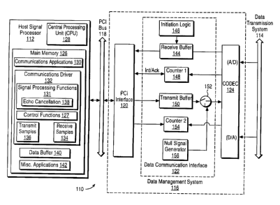
Now referring to Figure 1A, computer system 110 is shown having a host
signal processor (HSP) 112 communicating with a data transmission system 114
via
-10-
SUBSTITUTE SHEET (RULE 26)
CA 02380686 2002-O1-29
WO 01/11831 PCT/US00/21310
data management system 116. HSP 112 is connected to peripheral component
interface (PCI) bus 118, which connects the HSP to various peripheral
components
including data management system 116. Data management system 116 includes PCI
interface 120 that communicates on the PCI bus 118 using a PCI standard
protocol for
transmitting data on the PCI bus. Such a protocol is standard in the industry
and well
known to those skilled in the art. The PCI interface 120 communicates with the
data
communication interface 122 to receive and send data from the data
transmission
system. A signal converter also known as a CODEC 124 receives analog signals
from
the data transmission system 114 and converts them to digital data signals
that are
recognizable by the data communication interface 122 for ultimate transfer to
the HSP
112. The CODEC 124 also converts digital data signals received from a data
communication interface 122 to analog signals that are recognizable by the
data
transmission system 114. Data transmission system 114 is a system that
transfers data
in the form of analog signals and can include a conventional telephone system
that is
commonly used by data management systems such as the invention.
The following is a description of data management system 116 in accordance
with one embodiment of the invention that functions with HSP modem software as
a
modem to connect HSP 112 to data transmission system 114. As discussed above,
the
modern modem is no longer a single unit that performs all modem functions. The
control functions of the modem are now done by the HSP 112 and the data
transfer
operations are performed in data communications interface 122, which acts to
connect
HSP 112 to data transmission system 114.
HSP 112 includes a main memory 126 that is controlled by a central processing
unit (CPU) 128 to perform data transfer and data processing functions, among
other
functions. Main memory 126 includes communications applications 130 to perform
functions including but not limited to file transfer, Web browsing, and E-mail
access.
Communications applications 130 may also include applications to implement
SUBSTITUTE SHEET (RULE 26)
CA 02380686 2002-O1-29
WO 01/11831 PCT/US00/21310
networking protocols such as Point to Point Protocol (PPP), which is well
known to
those skilled in the art. Communications driver 132 includes software programs
to
receive samples 134, transmit samples 136 and perform signal processing
functions
and control functions127 including echo cancellation 138. Main memory 126
further
includes data buffer 140 and miscellaneous applications 142, which share the
central
processing unit 128, main memory 126, and other resources of HSP 112.
Still referring to Figure 1A, data communication interface 122 includes a
receive buffer 144 that communicates with the CODEC 124 to receive data from
the
data transmission system 114 as converted to digital signals by the CODEC 124.
Receive buffer 144 further communicates with the PCI interface 120 to send
data at the
request of the HSP 112. Data communication interface 122 further includes
initiation
logic 146, communicating with the receive buffer 144 and configured to perform
logic
operations to initiate communication between the CODEC 124 and receive buffer
144.
The HSP 112 initializes both the receive and transmit buffers 134,136 using a
control
register (not shown).
First counter 148 communicates between the CODEC 124 and PCI interface
120, and ultimately to HSP 112, to keep track of data transferred in and out
of the
receive buffer 144. In operation, the initial state is such that the receive
counter 148 is
set to the physical size of the buffer, and the transmit counter 154 is set to
zero. In this
state, the receive buffer is "full" and the transmit buffer is "empty." The
initiation
logic is used to reset the state of the interface buffers 144,150. In its
initial state, the
receive buffer 144 is full of "null" samples, which represent an analog
waveform
having no energy. By reading the first counter 148, the HSP 112 is notified
that the
receive buffer 144 is full of null samples to be transferred and that the
transmit buffer
150 has space for up to a full buffer of samples. This will be discussed in
further detail
below.
-12-
SUBSTITUTE SHEET (RULE 26)
CA 02380686 2002-O1-29
WO 01/11831 PCT/US00/21310
Data communication interface 122 further includes a transmit buffer 150 that
communicates with the PCI interface 120 to receive data from the HSP 112.
Transmit
buffer 150 also communicates with data switch 152 and transfers data stored in
the
transmit buffer to CODEC 124 when the switch is in the position connecting the
two,
where it is converted from a digital data signal to an analog data signal for
transmission
to the data transmission system 114. The data is then transferred to a
destination which
can be another HSP connected to a similar data management system or any other
device that can use the data. Data communication interface 122 can further
include a
second counter 154 that communicates with the PCI interface 120 and CODEC 124
to
track data received by and transferred from the transmit buffer 150. The
second
counter 154 is further connected to null signal generator 156, which is
further
connected to switch 152. The switch 152 is configured to alternately connect
the
transmit buffer 150 with the CODEC 124 or the null signal generator 156 with
the
CODEC 124.
Still referring to Figure 1A, in operation, data is received from a data
transmission system 114 by the CODEC 124 and converted from an analog signal
to a
digital data signal. At the beginning of the communication connection, the
initiation
logic 146 initiates the receive buffer 144 to receive the digital data signal
and store it in
the form of digital data in the receive buffer 144. Referring to Figure 3, a
diagrammatic view of data flow is shown to illustrate how the data is
transferred and
categorized. Data is transferred in a serial manner and grouped into samples
310,
which can be of any length, such as 16 bits of digital data. Referring again
to
Figure 1A, this stream of data samples 310 enters one end of the receive
buffer 144 in a
first-in/first-out (FIFO) manner, with the data exiting another end of the
receive
buffer. The data is then transferred to the PCI interface 120 and, ultimately,
to the host
signal processor 112. Typically, the host signal processor 112 transfers data
in groups
of samples 312.
-13-
SUBSTITUTE SHEET (RULE 26)
CA 02380686 2002-O1-29
WO 01/11831 PCT/US00/21310
Referring to Figures 4 and 5, the storage operation in the receive buffer 144
is
illustrated in more detail. The sizes and lengths of the buffers described
below and
illustrated in Figure 4 and 5 are for illustration only. Other buffer sizes
can be used in
accordance with the invention. For proper handling of overflow conditions, the
counter must have a range greater than the length of the buffers. This allows
the
counter to track the number of samples lost as well as those transferred, so
the echo
cancellation procedures can operate seamlessly in the case of buffer overflow.
A threshold is programmed for the counter by a designer and may be based on a
number of factors. The threshold may also be different for different
communication
standards, and for different points in the procedures described by the
communication
standards. One factor is the minimum number of samples that the HSP is
configured to
handle at one time, which should be taken into account to realistically
predict the
amount of data to be transferred to the HSP so that interrupts will not occur
too
frequently. If this number is too small, for example, the HSP will be
overloaded with
more interrupts in which it can effectively respond. This is an improvement
over the
prior art systems that interrupt the HSP whenever data is available,
overloading the
HSP with interrupt signals. According to one embodiment of the invention, the
HSP is
burdened with only interrupt at a time until it responds or acknowledges the
interrupt,
thereafter, allowing for another interrupt to be sent.
The length of the buffer and the threshold can be designed to balance certain
competing parameters such as the delay incurred from the data passing through
the
buffer, the probability of buffer overflow and the frequency of interrupts. If
the
threshold is set properly, the HSP can have a latency of several samples
before it must
respond to the interrupt. The buffer is then less likely to overflow.
In Figure 4, a diagrammatic view of data transfer in the receive buffer 144 is
illustrated in accordance with the invention. In Figure 5, diagrammatic view
of the
counter 148 and respective locations of the counter's pointer in a relation to
different
-14-
SUBSTITUTE SHEET (RULE 26)
CA 02380686 2002-O1-29
WO 01/11831 PCT/US00/21310
data transfers into the buffer is illustrated. Figure 4 further illustrates a
buffer 144
having 128 locations for storing 128 samples of data, where two transfers of
sixteen
samples each occur to a buffer sized to hold 128 samples. The samples stored
in the
buffer 144 of Figure 4 illustrate data samples stored in locations 32-127.
These
represent the locations immediately following two groups of samples
transferred out of
the buffer while none are received, leaving room for the CODEC to transfer 32
more
samples to empty locations 0-31.
Referring to Figure 5, with reference to Figure l, upon the initiation of the
receive buffer 144 by initiation logic 146, the counter is reset to 128. Each
time a
sample is received, the counter is incremented by one. When data is
transferred from
the receive buffer 144, the counter is decremented according to the number of
samples
that are transferred from the buffer. As illustrated in the counter grid, the
counter is
configured to count down to 0 and up to 255. If the pointer were reduced down
to 0,
this would indicate that the buffer is empty, or, in other words, 128 samples
of data
were transferred from the buffer and none were received from the CODEC 124. If
the
pointer was located at position 128, this would indicate that the buffer is
full, or, in
other words, that 128 samples of data were transferred to the buffer from the
CODEC
and none were transferred to the PCI interface 120. Location P, indicates that
two
groups of 16 samples each were transferred. Unless data is read, the data will
begin to
be overwritten in the buffer by incoming data. Location P,, occurring
subsequent in
time to position P,, indicates that a total of 33 samples were received by the
buffer and
none were transferred to the PCI interface 120.
Referring again to Figure 4, a situation is illustrated where 96 samples of
data
are stored in positions 32-127 and 33 samples are transferred from the CODEC
to the
buffer. This is an overflow condition since one sample was transferred after
the buffer
was full at 128 samples. In this example, the receive buffer 144 is initially
at a full
condition. This could be due to either initialization of the data
communication interface
-15-
SUBSTITUTE SHEET (RULE 26)
CA 02380686 2002-O1-29
WO 01/11831 PCT/US00/21310
122 by the HSP 112, or latency in responding to an interrupt. Once the HSP 112
responds to the interrupt from the counter 154 and transfers 32 samples from
positions
0-3 l, the counter is moved to position P 1 as shown in Figure 5. The counter
is reduced
to 96, and positions 32-127 (Figure 4) have valid samples. Assuming the HSP
112
stops transferring samples and acknowledges the interrupt at this point,
another
interrupt will be generated if the threshold is set lower than 96. In this
example (Figure
4), the HSP 112 is busy, so before it has a chance to respond, 33 samples are
transferred from the CODEC 124. Now the counter 154 is at 129, indicating that
one
sample has been overwritten. When the HSP 112 begins to respond to interrupts
again,
it will read an invalid sample where the new sample has overwritten an old one
. The
last sample from the CODEC overwrites position 32, which is the first sample
in
Sample Group 3, which has not yet been processed by the HSP. This will cause
some
noise in the signal received by the HSP 112. In this example, the counter 154
ranges
from 0-255, so it can indicate up to 127 lost samples.
The counter has a range that is greater than the size of the physical buffer,
adding greater flexibility to the buffer over the prior art. The counter
capacity defines
the limits of the virtual size of the buffer. This does not mean that data can
fill the
buffer beyond its physical limits, but the counter keeps track of the number
of samples
transferred in and out of the buffer, so that the delay seen by the echo
cancellation
procedures is consistent. The counter is limited in practice to a finite size
and therefore
has a maximum value. A mechanism is needed to handle an overflow of the
counter.
One such mechanism would allow the counter to wrap around to its minimum value
when it is incremented from its maximum value. This could cause the situation
where
the HSP responds to an interrupt, but finds that the counter indicates a value
less than
the threshold. To prevent this, a sticky bit can be used to handle counter
overflow. In
this configuration, the most significant bit of the counter is a sticky bit.
Thus, once it
becomes logic one, it can only become zero again through a decrement. That
way, if
-16-
SUBSTITUTE SHEET (RULE 26)
CA 02380686 2002-O1-29
WO 01/11831 PCT/US00/21310
an increment is done to the counter when it is at its maximum value, the next
value will
be half the maximum value instead of the minimum value. For example, if an 8
bit
counter is used and is incremented from a value of 255, the next value would
be 128
instead of 0.
Referring now to Figure 1B, a block diagram of a HSP based modem in the
context of Quadrature Amplitude Modulation (QAM) will now be described. QAM is
a method that changes the phase and amplitude of a carrier signal at a fixed
rate. In
one embodiment, the function blocks shown in the HSP 112 are performed by the
communications driver 132 of Figure 1A. Data from the modem controller is
mapped
onto two dimensional constellation points 160 using encoding methods described
by a
communications standard, such as V.22, V.22bis, V.32, V.32bis, or V.34. These
points, A; + j *B ; , where j is defined as the imaginary number equal to the
square root
of-1, are multiplied by a complex earner e'"'' . The real number portion of
the result is
used. The real number portion of the result represents a digital waveform,
which is
passed through a shaping filter 164, then sent to the data management System
116 to
be converted to an analog waveform and transmitted on the data transmission
system
114.
Incoming samples from the interface hardware are passed through a high-pass
filter 166 to remove DC components. For communication standards where the
transmit and receive directions use overlapping frequency bands, such as V.32,
V.32bis, and V.34, an echo-canceller 168 subtracts from this signal a filtered
and
delayed version of the output of the QAM 162 in the transmitter. The filter
and delay
parameters are typically set in the HSP during the startup procedures of the
communication standard. Next, an automatic gain control (AGC) 170 applies a
gain
such that the signal power is normalized to a preset level, regardless of the
attenuation
of the signal of the data transmission system 114. Next, a timing recovery
procedure
172 synchronizes to the symbol rate of the remote source of the data
transmission (the
-17-
SUBSTITUTE SHEET (RULE 26)
CA 02380686 2002-O1-29
WO 01/11831 PCT/US00/21310
remote transmitter) symbol rate. An equalizer filter 174 is then applied to
remove the
effects of inter-symbol interference (ISI). The equalizer operates on both the
in-phase
and quadrature portions of the signal, and outputs a two-dimensional complex
signal,
which can be demodulated by a demodulation and complex carrier phase locked
loop
(PLL) 176. A phase locked loop is used to ensure that the receiver's carrier
is
synchronized to the remote transmitter's carrier signal. Finally, the complex
output of
the demodulator is decoded by the Constellation Decoder 178 into information
bits
using the appropriate methods from the communication standard, and passed to
the
control functions for further processing and decoding 127.
Under the V.90 recommendation, one direction, upstream (or client to server)
uses QAM, and the other direction (downstream, or server to client) uses Pulse
Coded
Modulation (PCM). The configuration for a V.90 client is very similar to the
QAM
block 162of Figure 1B, except that there is no Demodulation and Carrier PLL
block
176, since there is no downstream carrier signal. In this case, the equalizer
is one
dimensional and its output is real. V.90 servers, on the other hand, are
different since
they do not use QAM techniques in the transmitter and they do not employ a
CODEC.
An overflow condition as disclosed above occurs when the host computer fails
to service the interface buffer 116 in time. The result is that some of the
samples in the
receive buffer are lost, and some null samples are transmitted to the CODEC
124.
However, the host continues to process samples normally, and the signal flow
is the
same as described above. The result is that some of the samples transferred to
the
high-pass filter are not representative of the analog signal being received
from the data
transfer system. And the signal used for echo-cancellation is not exactly that
which
was actually transmitted since it does not account for the null samples.
However, the
echo delay remains the same, so that HSP processes, including echo
cancellation,
continue to function smoothly in the case of an overflow. The effects of lost
samples
can be analyzed as "impulse noise", or noise having high power for a very
short
-18-
SUBSTITUTE SHEET (RULE 26)
CA 02380686 2002-O1-29
WO 01/11831 PCT/US00/21310
duration. Impulse noise can have many effects, depending on severity. For
example, it
can cause error in the data that is transmitted to the controller. Usually an
error-
correcting standard, such as V.42, is incorporated in the overall design, so
this effect
will be mitigated. Impulse noise may also cause one of the modems to initiate
rate
renegotiation or retrain procedures. Rate renegotiation procedures are
typically fairly
quick, less than one second, and may be unnoticeable by the communication
application in many cases. Full retraining of the system may take several
seconds, and
is more noticeable. The overall system incorporating the invention is designed
so that
overflow happens infrequently. Therefore, retraining due to overflow rarely
occurs.
The counter 148 is preprogrammed with a threshold which, when reached,
initiates an interrupt to be sent to the HSP 112 indicating that an overflow
condition is
imminent. In order to avoid losing data, the threshold can be set at a counter
location
equal to or less than 128 (Figure 5) so that the HSP can retrieve data prior
to an
overflow condition. In order to avoid a large amount of interrupts sent to the
HSP 112,
the counter can be configured to send interrupts one at a time and only after
a prior
interrupt has been acknowledged by the HSP 112. This feature is unlike
conventional
interfaces, which send interrupts each time data is received by a receive
buffer. In such
a conventional configuration, the HSP 112 is constantly interrupted when data
is
available. In another embodiment of the invention, there is no interrupt, but
the HSP
periodically reads the counter to determine whether there is enough data
available to
process.
For example, referring again to Figure 4, if the threshold of the counter 148
is
set to a number less than 96, an interrupt would be sent to the HSP 112 before
the
33 samples are received in the buffer. At this time, if possible, the HSP 112
can read
data from the buffer, making room for all 33 samples in the buffer and
avoiding an
overflow condition and preventing the loss of any samples.
-19-
SUBSTITUTE SHEET (RULE 26)
CA 02380686 2002-O1-29
WO 01/11831 PCT/US00/21310
The transmit buffer 150 receives and sends data in a similar manner as the
receive buffer 144. Data is received in the transmit buffer 150 in a first-in,
first-out
(FIFO) manner so that data is received in a serial manner at one end and
transferred out
in a serial manner at another end. The second counter 154 keeps track of data
entering
and leaving transmit buffer 150 in the same manner as the first counter 148
operates.
The second counter is synchronous with the first counter to ensure that both
buffers
operate at the same sample rate. The condition that is problematic for the
transmit
buffer is an underflow condition, which happens at the same time the receive
buffer 144 experiences an overflow condition. Underflow means that the CODEC
needs new samples for conversion, but none are available in the transmit
buffer 150.
The CODEC typically uses a single sampling rate for both A/D and D/A
conversion. Therefore, data is transferred from the receive buffer to the PCI
interface
at the same rate as data is transferred from a PCI interface to the transmit
buffer 150,
with a slight latency in time. Thus, the HSP must keep the number of samples
sent to
the transmit buffer 150, which is equal to the number of samples read from the
receive
buffer. So long as data is available in the transmit buffer 150, the switch
152 connects
the output of the transmit buffer 150 to the CODEC 124 so that data can be
transferred.
However, in the event of an underflow, when new data is not available in a
transmit
buffer, the switch 152 connects to null signal generator 156 to send a null
signal to the
CODEC 124. The null signal is then converted to an analog null signal sent to
the data
transmission system. This is in contrast to the conventional modem described
above,
in which the CODEC converts old samples that are leftover in the transmit
buffer from
prior transfers. Neither method will suffice to keep a reliable communication
link
active for long, so the system must be designed to minimize the occurrence of
overflow/underflow conditions.
Referring now to Figure 2, a second embodiment of the invention is illustrated
having a single counter circuit. The receive buffer 144 and transmit buffer
150 operate
-20-
SUBSTITUTE SHEET (RULE 26)
CA 02380686 2002-O1-29
WO 01/11831 PCT/US00/21310
in the same manner as the configuration illustrated in Figure 1. The switch
152 also
operates in the same manner. The new counter 210, however, is configured to
perform
the functions of the first and second counters 148, 154 in Figure 1. The
counter 210
receives data from the PCI interface 120 and CODEC 124 to keep track of data
that is
received by and sent from each of the buffers 144, 150. Conceptually, the size
of the
counter has a dual meaning: both the number of receive samples available for
processing by the HSP, and the number of spaces available to store transmit
samples
from the HSP. In practice, the counter may be connected to only one of the
buffers. In
this case, if the transmit and receive transfers do not occur simultaneously,
then the
counter has its dual meaning only after both transfers are complete. The
counter 210
is further connected to switch 152 to connect the transmit buffer 150 to the
CODEC 124 when data is available in the transmit buffer 150 to be transferred
to the
CODEC 124. The counter is further configured to connect the null signal
generator 156 to CODEC 124 when data is not available, sending a null signal
to the
data transmission system 114.
Refernng now to Figure 6A, a diagrammatic view of a conventional circuit of a
prior art configuration is illustrated for contrast. Circuit 610 includes a
first receiving
buffer 612 that is divided up into predetermined fields of predetermined
lengths. A
counter 614 is connected to the buffer 612 and is configured to send
interrupts to the
host processor each time a field of data is transferred to the buffer 612. In
operation,
the CODEC receives an analog signal, converts it to a digital data signal and
transfers
it to the buffer 612 in one of the two fields in which the buffer is divided.
The counter,
recognizing that predefined number of sample periods has passed, sends an
interrupt to
the host processor indicating that data is available.
The host processor 616 can then retrieve data from the address at which it was
left. Unlike the invention, the buffer 612 of this conventional configuration
receives
and transfers data in field blocks, sending and replacing fields of data. In
the event of
-21-
SUBSTITUTE SHEET (RULE 26)
CA 02380686 2002-O1-29
WO 01/11831 PCT/US00/21310
an overflow, an entire field of data can be lost when the host processor 616
is unable to
retrieve the data. The data transfer system 618 must keep a communication
link,
having a continuous signal going from the CODEC 611, to the receive buffer
612, to
the host processor 616, through the transmit buffer 620, back through the
CODEC 611
and ultimately back to the data transfer system 618. If data is transferred to
the receive
buffer 612 and host processor 616 is unable to receive data, the data
subsequently
transferred from the CODEC will overwrite an entire field of data. This
illustrates one
advantage of the invention in which only an absolute minimum amount of data is
lost
as a result of an overflow condition. Secondly, another aspect of the
invention that is
superior to this conventional configuration is the overflow handling counter
circuit.
The counter circuit of the prior art only serves to count sample periods, in
order to
generate periodic interrupts. The counter circuit of the above-described
embodiments
of the invention keeps track of the exact number of samples available and, due
to its
extended range, can account for lost samples due to overflow. In this prior
art
configuration, separate overflow and underflow circuits are needed, along with
counters to keep track of the number of frames lost, so the HSP knows which of
the
two buffer partitions to use. In contrast, the invention has a much more
simplified
circuit.
In further accordance with the invention, another feature can be included
wherein the interrupt rate can be made dynamic, based on the ability of the
HSP 112 to
respond. A nominal interrupt rate is established by setting the threshold to
the
minimum number of samples that the HSP 112 can handle at one time. As long as
the
HSP 112 can respond quickly enough, it will transfer samples and acknowledge
the
interrupt before the next minimum number of samples is available. However, if
the
HSP 112 takes twice as long to respond for example, it will find that the
counter
indicates that two groups of samples are ready for processing. The HSP 112 can
transfer both groups of samples for processing, so the next interrupt will not
occur until
-22-
SUBSTITUTE SHEET (RULE 26)
CA 02380686 2002-O1-29
WO 01/11831 PCT/US00/21310
another group of samples is available. If the HSP 112 continues in this
manner,
interrupts will only occur at half the nominal rate. In general, the rate of
interrupts in
the above-described embodiments will be dynamically matched to the rate at
which the
HSP 112 can handle them. This is in sharp contrast to the prior art, where
interrupts
occur at a fixed periodic rate, which increases the interrupt rate.
Furthermore, the loss
of data in this conventional configuration is not automatically accounted for
for
purposes of echo cancellation. If data is lost, it is completely written over
and not
accounted for by the counter, which only ranges to the length of the field of
samples.
In this event, complicated logic is needed in the host processor to account
for the lost
data for purposes of echo cancellation. These complicated algorithms are not
required
by a circuit employing the invention.
Referring now to Figure 6b, a sample data transfer in a circuit of Figure 6a
is
illustrated. Samples from the CODEC are put in the buffer 612 in a circular
manner.
When one field is full, the host processor will be interrupted. If the host
fails to
respond before it is time to put another sample in that field, the entire
field will be lost.
For example, if the CODEC has a sample available to be put in location 64 in
the
diagram, but the host has still not processed the previous data in Field 2,
all of that data
will be lost and replaced by new samples from the CODEC. In this case, the
echo
cancellation process would need to account for the lost samples.
Unlike conventional buffer schemes, the invention does not require the echo-
canceller to be deactivated, or the buffer to be flushed in the case of buffer
overflow.
The host, or non-real time part of the system, continues to operate as if
nothing
happened. The effect is that the echo-canceller buffer (not shown) would
contain a
signal that was not actually transmitted since a null signal was transmitted
when the
real signal was not available in time. As a result, the output of the echo
cancellation
logic, which is to be subtracted from the received signal, is noisy.
Therefore, the signal
passed to the timing recovery and equalizer blocks will be noisy. The result
is a buffer
-23-
SUBSTITUTE SHEET (RULE 26)
CA 02380686 2002-O1-29
WO 01/11831 PCT/US00/21310
scheme that is easier to implement than the conventional system, without the
need for
excessive logic to account for loss of samples in the echo cancellation
scheme.
The interface includes a flexible buffer system that efficiently transfers
data
between a host signal processor and a data transfer system, that enables a
data
processing system to receive data at different carrier frequencies and symbol
rates, and
that conforms with the V.34 and V.90 recommendations. Although this embodiment
is
described and illustrated in the context of a modem for a computer system, the
scope of
the invention extends to other applications where efficient data transfer
between real-
time and non-real-time systems is useful. Furthermore, while the foregoing
description
has been with reference to particular embodiments of the invention, it will be
appreciated that these are only illustrative of the invention and that changes
may be
made to those embodiments without departing from the principles of the
invention, the
scope of which is defined by the appended claims.
-24-
SUBSTITUTE SHEET (RULE 26)