Note: Descriptions are shown in the official language in which they were submitted.
CA 02380707 2002-04-23
y
-1
SEMICONDUCTOR DEVICE EVALUATION APPARATUS AND
SEMICONDUCTOR DEVICE EVALUATION PROGRAM PRODUCT
BACKGROUND OF THE INVENTION
Field of the Invention
The present invention relates to a semiconductor
device evaluation apparatus and particularly, to a
semiconductor device evaluation apparatus for evaluating an
electromagnetic near-field strength of a semiconductor
device. The present invention further relates to a
magnetic field sensor suitable for use in the semiconductor
device evaluation apparatus. The present application is a
divisional of Serial No. 2,275,781, filed June 18, 1999.
Description of the Prior Art
EMI (electromagnetic interference) evaluation of
electronic equipment is to measure an emitted
electromagnetic far-field strength of the electronic
equipment according to measurement methods stipulated in
various standards and evaluate whether or not an emission
quantity meets a standard. If the standard is not met,
further detailed evaluation is performed at levels of a
case and a printed circuit board of the electronic
equipment as evaluation objects in order to specify a
problematic part in the equipment.
In a fundamental evaluation method, electrical
parameters such as a current, voltage and an
electromagnetic near-field and the like at various parts of
an equipment are measured by proper means and a part which
CA 02380707 2002-04-23
. ~ . .
_7_
has a possibility to cause a problem in terms of
electromagnetic compatibility is thus specified. For
example, in Japanese Patent Application Laid-Open No. 4-
230874, there is disclosed a method in which a two-
s dimensional electromagnetic strength measurement apparatus
is employed, a printed circuit board built in an electronic
equipment is extracted therefrom, a magnetic field sensor
is disposed in the vicinity of the printed circuit board,
a two-dimensional magnetic field distribution is measured
in a plane which is parallel to the board and it is
eventually evaluated that a part where a high magnetic
strength is measured has a high possibility of being a
noise source.
In such a conventional example, in many cases, there
has been adopted a method in which, at first, a problematic
part and a mechanism of a problematic circuit function are
selected by narrowing candidates from a list thereof
according to experiences and expertise of a person in
measurement and an optimal EMC countermeasure is attained.
For a countermeasure in an EMC, it is important to conduct
non-contact measurement in order to suppress, to the lowest
level possible, an electrical influence on a circuit
function of the electronic equipment which is an evaluation
object. When a semiconductor device itself (for example,
a semiconductor package) as an object for evaluation is, in
a non-contact manner, measured to specify an internal
problematic part as in the case of electronic equipment,
there arises a necessity for an electromagnetic sensor with
CA 02380707 2002-04-23
1 v v
-3-
a spatially high resolving power.
However, a practical electromagnetic sensor adaptable
for a semiconductor device has not been known.
As a noise evaluation method of a semiconductor
S device, there is available a document: "Electromagnetic
Emission (EME) Measurement of Integrated Circuits, DC to 1
GHz" IEC 47A/429/NP NEW WORK ITEM PROPOSAL, 1996.2,
published by IEC in which a measurement method for emission
noise from a semiconductor device is shown. Besides, three
is also available a document: "Electromagnetic
Compatibility Measurement Procedures for Integrated
Circuits" IEC 47A/428/NP NEW WORK ITEM PROPOSAL, 1996.2,
published by IEC in which a measurement method for
conduction noise which occurs in each pin of a
semiconductor device is shown.
Two measurement methods for an emission noise from a
semiconductor device package are shown. In the first
measurement method, a semiconductor device which is an
object for evaluation is mounted on a surface of a printed
circuit board and peripheral circuitry for operating the
semiconductor device is constructed on the rear surface
thereof. The printed circuit board is fixed on a plane in
the top portion of a TEM cell so that a surface of the
printed circuit board on which a semiconductor device is
mounted resides in the inside of the Transverse
Electromagnetic (TEM) cell. One end of the TEM cell is
constructed as a reflection-free terminal and the other end
CA 02380707 2002-04-23
-4-
connected to a spectrum analyzer, and thereby emission
noise from the semiconductor device only can be measured
excluding influences from the peripheral circuitry.
A second method is shown below. A semiconductor device
as an object for evaluation is mounted on a surface of a
printed circuit board and peripheral circuitry for
operating the semiconductor device is constructed on the
rear surface thereof . The printed circuit board is provided
with the surface on which the semiconductor devices are
mounted facing upward and a shielded loop constructed from
a semi-rigid coaxial cable is arranged above the printed
circuit board. The vicinity of the semiconductor device is
scanned with the shielded loop along a plane parallel to
the printed circuit board by a scanner mechanism and
thereby only the emission noise from the semiconductor
device can be measured. In this case, the maximal value of
outputs at measurement sites is evaluated as a problematic
site to specify.
Then, a measurement method for conduction noise which
occurs in each pin of a semiconductor device package will
be shown below. A structure comprises a test board for
mounting a semiconductor device which is an object for
evaluation and a main board for connecting the test board
and a spectrum analyzer thereby. The semiconductor device
is mounted in the center of the circular test board and the
test board is attached to the main board in the center
thereof. Interconnects are provided on each of the two
CA 02380707 2002-04-23
-S-
boards radially toward the outside of the board and
conduction noise from the pins of the semiconductor device
is measured by the spectrum analyzer which is connected to
the pins through connectors of a coaxial type mounted in
the vicinity of the outer periphery of the main board.
As other examples, the following methods are named.
For example, in Japanese Patent Application Laid-Open No.
64-65466, there is disclosed an identification method for
an electromagnetic field noise generating part in which a
reference plane is imagined which intersects electronic
equipment, an arbitrary plane which is in parallel with the
reference is scanned with an antenna, strengths of
electromagnetic field noise and noise generating sites are
sampled, and thereby a generation distribution map for
electromagnetic noise of the electronic equipment as viewed
from the arbitrary plane set in advance is expressed in the
form of a contour map. Besides, in Japanese Patent
Application Laid-Open No. 5-119089, there is disclosed an
electromagnetic radiation visualization apparatus, in which
a variable-length dipole antenna of a measurement unit is
fixed in length which matches a measurement frequency and
the antenna is moved by a three-dimensional movement
mechanism in an anechoic electromagnetically chamber while
scanning. At this point, the interior of the
electromagnetically anechoic chamber is optically made dark
and a brightness of a lamp which is proportional to an
electric field strength at each measurement site is
CA 02380707 2002-04-23
. ~ "
-6-
recorded by a sterocamera with exposure. Furthermore, in
Japanese Patent Application Laid-Open No. 6-58970, there is
disclosed an invention having an object to provide an EMI
measurement apparatus which can three-dimensionally measure
noise along X-Y-Z directions on the front side of a print
wiring board on which electronic parts with much of
unnecessary radiatian are mounted, and which can two-
dimensionally measure noise along X-Y directions on the
rear side thereof. This is an EMI measurement apparatus
which has a construction in which a print wiring board is
set to an antenna for measuring an interference in which
winding coils are arranged in an array and a magnetic near-
field probe is mounted on the fore end arm of a robot which
can be driven along X-Y-Z directions on the front side of
the print wiring board in order to measure a noise
generating source of the print wiring board on which an
electronic part which is rich in unnecessary radiation is
mounted, whereby a distribution of magnetic field strengths
in unnecessary radiation on both sides, front and rear, is
measured. In addition, in Japanese Patent Application
Laid-Open No. 9-80098, there is disclosed an EMC probe, by
which a spatial resolving power is increased and a
measurement band region is sufficiently secured. This
comprises a flexible board whose surface is insulated and
a winding with a single turn or a plurality of turns for
detecting a magnetic near-field vector of an object for
measurement, while being disposed obliquely, the winding
CA 02380707 2002-04-23
r ~,
_7_
being constructed from a metal thin film formed in a
plane on the board.
BRIEF SUMMARY OF THE INVENTION
Object of the Invention
Problematic points of a measurement method for
emission noise from a semiconductor device package will be
described below. First of all, problematic points of a
method using a TEM cell will be described.
A first problematic point is that there is available
no detailed standards for designing of a printed circuit
board on which a semiconductor device is mounted and thus
an evaluation result depends on a design of the print
circuit board. Besides, since a printed circuit board on
which a semiconductor device is mounted is square, there
can be four ways to mount the semiconductor device, but a
result is different according to a way it is mounted.
The reason why is considered that an electromagnetic
wave emitted from a surface of a printed circuit board on
which a semiconductor device is mounted has a polarized
wave and a pin position whose emission is large in quantity
is changed, whereby emission characteristics are largely
changed.
A second problematic point is that if a quantity of
emission noise exceeds a tolerable level, though the
emission noise can correctly be measured, a countermeasure
is required. However, this method is very had to
specifically locate a problematic site.
CA 02380707 2002-04-23
a . s
The reason why is that since the semiconductor device
is present in the TEM cell, it is impossible to correctly
confirm what part of the semiconductor device has a
problem.
A third problematic point is that a printed circuit
board is required to be prepared for each semiconductor
device for evaluation, which entails cost in terms of time
and economy.
A fourth problematic point is that since the
semiconductor devices are evaluated under constant
conditions, evaluation results have chances in which the
results are not effective for use conditions by a user.
In addition, problematic points of a method using a
shielded loop will be described.
A first problematic point is that there is available
no detailed standards for designing of a printed circuit
board on which a semiconductor device is mounted and thus
an evaluation result depends on a design of the printed
circuit board.
The reason why is considered that an electromagnetic
wave emitted from a surface of a printed circuit board on
which a semiconductor device is mounted has a polarized
wave and thereby emission characteristics are largely
changed.
A second problematic point is that if a quantity of
emission noise exceeds a tolerable level, though the
emission noise can correctly be measured, a countermeasure
CA 02380707 2002-04-23
a , t
-9-
is required. However, this method is very hard to
specifically locate a problematic site.
The reason why is that a small-sized type is hard to
be realized since the shielded loop is prepared by a semi-
s rigid coaxial cable and as a result, a structure has an
insufficient spatial resolving power and it is impossible
to correctly confirm what part of a semiconductor device
has a large emission.
A third problematic point is that a printed circuit
board is required to be prepared for each semiconductor
device for evaluation, which entails cost in terms of time
and economy.
A fourth problematic point is that since the
semiconductor devices are evaluated under constant
IS conditions, evaluation results have chances in which the
results are not effective for use conditions by a user.
Furthermore, problematic points of a measurement
method for conduction noise which occurs in each pin of a
semiconductor package will be described below.
A first problematic point is that since electrical
connection between the test board and the main board
depends on point contact formed by pressure bonding of
metal pin, transmission characteristics come to be in
disorder under a high frequency band close to 1 GHz.
The reason why is considered that an impedance becomes
discontinuous in the point contact portion.
A second problematic point is that a test board has to
CA 02380707 2002-04-23
a a r
_ 10-
be newly prepared for each semiconductor device for
evaluation, which entails cost in terms of time and
economy.
A third problematic point is that since the
semiconductor devices are evaluated under constant
conditions, evaluation results have chances in which the
results are not effective for use conditions by a user.
A fourth problematic point is that evaluation of a
semiconductor device which requires circuitry with a large
construction is hard to be performed because of requirement
for a large space.
In this way, conventional examples have had
inconveniences that, firstly, it is hard to correctly
measure emission noise of a semiconductor device and
secondly, even if emission noise can be measured, it is
impossible to specify what part in the semiconductor device
is problematic.
Summary of the Invention
It is an object of the invention claimed in the parent
application Serial No. 2,275,781 to provide a magnetic
field sensor by which the above described inconveniences
which conventional examples have had are improved and
especially, emission noise of a semiconductor device can
correctly be measured. It is another object of the
invention of the parent application Serial No. 2, 275, 781 to
provide a semiconductor device evaluation apparatus with
good workability and high reliability which can perform EMI
CA 02380707 2002-04-23
-11-
evaluation of a semiconductor device. It is an object of
the present invention to provide a semiconductor device
evaluation program product stored in a storage medium for
evaluating an electromagnetic field from a semiconductor
device using a semiconductor device evaluation apparatus.
The parent application Serial No. 2,275,781, describes
and claims a semiconductor device evaluation apparatus
which comprises: an electromagnetic field measurement unit
for measuring an electromagnetic field distribution emitted
from a semiconductor device; an electromagnetic field
distribution extracting unit for extracting a distribution
of an electromagnetic field higher than a threshold value
determined in advance and postional information of the
distribution from an electromagnetic field distribution of
a semiconductor device which is measured by the
electromagnetic field measurement unit; and a part
specifying unit for specifying a part of an object for
measurement an electromagnetic field emitted from which is
high among parts of the object for measurement based on the
positional information of the electromagnetic field
distribution which is extracted by the electromagnetic
field distribution extracting unit. This allows the
objects described above to be attained.
The electromagnetic field measurement unit measures an
electromagnetic field distribution which is emitted from a
semiconductor device. Then, the electromagnetic field
distribution extracting unit extracts a distribution of an
electromagnetic field higher than a threshold value
CA 02380707 2002-04-23
-12-
determined in advance and positional information of the
distribution from an electromagnetic field of the
semiconductor device. The positional information may be,
for example, a distribution image in which information on
whether or not an electromagnetic field exceeds the
threshold is stored in a pixel corresponding to the
information. The part specifying unit specifies a part an
electromagnetic field of whose emission is high based on
the positional information of the electromagnetic field
distribution. For example, a part of a semiconductor
device such as an interconnect or a lead frame is
specified. Thus, evaluation of an electromagnetic field
emitted from the semiconductor device is effected.
According to an aspect of the present invention there
is provided a semiconductor device evaluation program
product stored in a storage medium for evaluating an
electromagnetic field from a semiconductor device, using a
semiconductor device evaluation apparatus including an
electromagnetic field sensor, far measuring a two
dimensional electromagnetic field distribution in a plane
parallel to the upper surface of the semiconductor device;
a computer to which an output of the electromagnetic field
sensor is supplied as an input; and a display for
displaying data supplied from the computer as an output;
the program causes a semiconductor device evaluation
apparatus to extract an electromagnetic field distribution
higher than a threshold value determined in advance from an
electromagnetic field distribution of a semiconductor
CA 02380707 2002-04-23
- 12a -
device measured by the electromagnetic field sensor;
convert the electromagnetic field distribution to a
distribution image in the two-dimensional plane; collate
the distribution image with a projected image of
interconnects and lead frames of the semiconductor device
which have been generated; and specify the interconnect or
the lead frame which is superposed on each other as an
emission source if the images of the electromagnetic field
distribution, and the interconnects and lead frames are
superposed on one another by the collation.
According to another aspect of the present invention
there is provided a memory for storing data for access by
a computer comprising: semiconductor device evaluation data
stored in the memory; the data includes pin assignment data
each of which shows a function in a circuit of a
corresponding lead frame of the semiconductor device;
electromagnetic field strength data which shows an
electromagnetic field strength which has been sensed by the
electromagnetic field sensor on each pin; and sets of order
data each set of which defines a level in the order of
electromagnetic field strength level for a pin
corresponding to the electromagnetic field strength data,
wherein the pin assignment data and the electromagnetic
field strength data are related with each other by a level
defined in the order according to the sets of order data.
BRIEF DESCRIPTION OF THE DRAWINGS
FIG. 1 is a block diagram showing a schematic
CA 02380707 2002-04-23
. .
- 12b -
configuration of a semiconductor device evaluation
apparatus according to the present invention;
FIG. 2 is a flowchart showing an example of processing
by the semiconductor device evaluation apparatus shown in
FIG. l;
FIGS. 3(A) to (D) are representations for illustrating
examples of images used in steps shown in FIG. 2, and FIG.
3(A) is a representation showing an example of a picked-up
image, FIG. 3(B) is a representation showing an example of
a distribution image, FIG. 3 (C) is a representation showing
an example of a collation image, and FIG. 3(D) is a
representation showing an example of a extracted image;
FIG. 4 is a block diagram showing a configuration of
an embodiment of the present invention;
FIG. 5 is a block diagram showing a configuration of
an electromagnetic field sensor and a measurement unit
shown in FIG. 4;
FIG. 6 is a perspective view showing a detailed
configuration of the multilayer magnetic field sensor shown
in FIG. 5;
CA 02380707 2002-04-23
. , _13_
FIG. 7 is a perspective view showing a construction to
improve a sensitivity of the multilayer magnetic field sensor
shown in FIG. 5;
FIG. 8 (A) is a diagram showing a layer configuration of
a multilayer magnetic field sensor having a reinforcement
base member on one side, and FIG. 8 (B) is a diagram showing
a layer configuration of a multilayer magnetic field sensor
having reinforcement base membersrespectively on both sides;
FIG. 9 is a perspective view showing a construction of
a multilayer magnetic field~sensor having a fourth layer;
FIGS. 10 (a) , (b) are front views showing configuration
of multilayer magnetic ffield sensors, and FIG. 10(a) is a
front view of a multilayer magnetic field sensor having a base
member at the lowest part and FIG. 10 (b) is a front view of
a multilayer magnetic field sensor having a plurality of base
members at the lowest part;
FIG. 11 is a front view of a multilayer magnetic field
sensor having a base member outside a C shaped pattern;
FIGS. 12 (a) to (f) are diagrams showing steps of a
fabrication process for a multilayer magnetic field sensor;
FIGS. 13(A), (B) are representations showing
measurement results of two-dimensional magnetic field
distribution, and FIG. 13(A) is a representation showing a
measurement result in the embodiment and FIG. 13(B) is a
representation showing a measurement results in a
conventional example;
CA 02380707 2002-04-23
-14-
FIGS. 14(A), (B) are graphs showing voltage vs.
magnetic field conversion characteristics of a multilayer
magnetic field sensor, and FIG. 14(A) is a graph showing
values of a calibration coefficient for an amplitude and FIG.
14 (B) is a graph showing values of a calibration coefficient
for a phase;
FIG. 15 is a plan view showing pin assignment of a
semiconductor device package for evaluation; and
FIG. 16 is a plan view showing a structure of a
conventional shielded loop y
DETAILED DESCRIPTION OF THE PREFERRED EMBODIMENTS
An embodiment of the present invention will be
detailed with reference to the accompanying drawings. FIG.
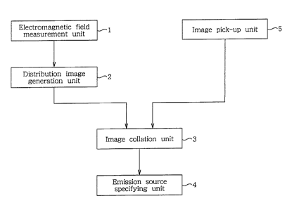
1 shows a configuration of the present invention. A
semiconductor device ,evaluation apparatus comprises: an
electromagnetic field measurement unit 1 for measuring a
two-dimensional electromagnetic field distribution in a
plane parallel to an upper surface of a semiconductor device;
a distribution image generation unit 2 for not only
extracting a distribution of an electromagnetic ffield higher
than a threshold value determined in advance from the
electromagnetic field distribution of the semiconductor
device measured by the electromagnetic field measurement unit
1 but converting the extracted electromagnetic field
distribution to a distribution image in a two-dimensional
plane; an image collation unit 3 for collating the
CA 02380707 2002-04-23
a -1 S-
distribution image generated by the distribution image
generation unit 2 with a projected image, generated in advance,
of an interconnect and a lead frame of the semiconductor
device; and an emission source specifying unit 4 for
specifying an interconnect or a lead frame whose images are
superposed, as an emission source if the images of the
electromagnetic field distribution, and the interconnects
and lead frames are superposed on each other in collation by
the image collation unit 3.
The electromagnetic field measurement unit 1, for
example, comprises: an electromagnetic field sensor 206 for
measuring a magnetic field in the vicinity of a semiconductor
device; a measurement unit 210 for measuring an emitted
electromagnetic field of the semiconductor device using the
electromagnetic field sensor 206; and a scan unit 207 for
scanning with the magnetic field sensor 206 in the vicinity
of the semiconductor device. The magnetic field sensor, in
a preferable embodiment, comprises: a signal layer having a
signal line; and a ground layer which is a ground for the signal
layer. In addition, the electromagnetic field measurement
unit 1 may further comprise an attenuator 47 connected to the
electromagnetic field sensor206foreliminating an influence
of either electric or magnetic field in measuring one of them.
FIG. 2 is a flowchart showing-an example of processing
by the configuration shown in FIG. 1. In the figure, numerals
respectively indicate constituents performing portions of
the overall processing. As shown in FIG. 2, as a pretreatment,
CA 02380707 2002-04-23
-16-
a lead frame of a semiconductor device for evaluation are
picked-up as an image (205) . An example of a picked-up image
31 is shown in FIG. 3(A). In the picked up image 31, a
semiconductor device chip 32 and a lead frame 33 are shown.
In addition, pin assignment information of the semiconductor
device is added to the image 31 as an input (213).
Then, a two-dimensional electromagnetic field '
distribution in the vicinity of the semiconductor device for
evaluation is measured (210). A threshold value for an
amplitude of an electromagnetic field is specified
automatically or by manual setting (211). Besides, a
distribution of electromagnetic field which exceeds the
threshold value is extracted (214 (a) ) . An example of an image
of the electromagnetic field distribution 34 is shown in FIG.
3 (B) . Then, the distribution image 34 is superposed on the
picked-up image 31 as shown in FIG. 3(C) (214(b)).
Furthermore, a lead frame whose images are superposed on each
other is extracted (214 (c) ) . An example of an extracted image
is shown in FIG. 3 (D) . Subsequently, a pin number of a lead
frame which has been extracted is identified (214 (d) ) and the
pin number is transmitted as an output . Not only pin numbers
but strengths of electromagnetic field of all the pins may
be transmitted as outputs in some embodiments.
In the embodiment in which~strengths of an
electromagnetic field of all the pins are transmitted as
outputs, the distribution image generation unit 2 is provided
with a function of segmenting an electromagnetic field
CA 02380707 2002-04-23
emitted from the semiconductor device between the maximum and
minimum strength level into a plurality of emission strength
level intervals. In this case, the emission source
specifying unit 4 is preferably provided with a function of
specifying an interconnect or a lead frame which corresponds
to each of the emission strength level intervals . Besides,
when emission strengths of lead frames are determined, the
emission source specifying unit 4 is preferably provided with
a function of not only rearranging lead frames in the order
of emission strength level interval, but also transmitting
the rearranged lead frame information in the new order of the
lead frames as an output to the outside. In order that
emission strengths of all lead frames are determined, a
strength level interval is narrowed till no change appears
in the-newer order of the lead frames after rearrangement.
In an embodiment, the emission source specifying unit
4 is provided with a function which transmits, as an output
to the outside, synthesized information of lead frames
rearranged according to the emissionstrengthlevel intervals
and pin assignment made by referencing to the pin assignment
database showing functions of the lead frames in a circuit .
Thus, evaluation data for the semiconductor device are
generated. Semiconductor device evaluation data provided to
a user according to the embodiment .comprises, in a preferred
embodiment : pin assignment data each of which shows a function
in a circuit of a corresponding lead frame of the
semiconductor device; electromagnetic field strength data
CA 02380707 2002-04-23
-18-
each of which shows an electromagnetic field strength which
has been sensed by the electromagnetic field sensor on each
piny and sets of order data. each set of which defines a level
in the order of electromagnetic field strength for a pin
corresponding to the electromagnetic field strength data:
Herein, pin assignment data and electromagnetic field
strength data are related with each other by a level in'the
order according to order data. According to data with such
a structure, pin assignment data showing pin functions and
electromagnetic field strengths are indicated in the
decreasing order of electromagnetic field strength. With
this data structure, a lead frame which is an emission source
can be specified with ease, when an emitted electromagnetic
field of the semiconductor device exceeds an allowable level,
information which is useful for a user to take measure to cope
with the case, can be supplied to the user since even a function
in circuit of a lead frame in question can be displayed.
Various functions of the distribution image generation
unit 2, the image collation unit 3 and the emission source
specifying unit 4 can be realized by a processing apparatus
such as a computer or the like. In this case, the processing
apparatus comprises: a central processing unit (CPU?;
a main storage unit, an input/output unit; an auxiliary
storage unit; and a display. Programs which are used for the
computer to execute the functions described above are stored
in the auxiliary storage unit. Storage of the programs to
the auxiliary storage unit may be effected through a
CA 02380707 2002-04-23
_19_
communication line in addition to a method in which the
programs are introduced from a storage medium such as a CD-ROM
or the like by way of the input/output control unit.
The programs comprise as commands to run on the
processing apparatus: a command extracting an
electromagnetic field distribution higher than a threshold
value determined in advance from an electromagnetic field
distribution in the vicinity of a semiconductor device
measured by the electromagnetic field sensor 206; a command
of converting the electromagnetic field distribution to a
distribution image in a two-dimensional plane; a command of
collating the distribution image with a projected image of
interconnects and lead frames of the semiconductor device
which have been generated; a command of specifying an
interconnect or a lead frame which is superposed on each other
as an emission source, if the images~of the electromagnetic
field distribution, and the interconnects and lead frames are
superposed on .one another by the collation. These commands
each of which forces a function to be executed include another
program which is used to have the computer realize a desired
function in dependence on the operating system and other
application programs of the processing apparatus. It is
needless to say that the processing apparatus may entirely
be controlled by the program onl_y~~
Various functions of the distribution -image generation
unit and the emission source specifying unit can be realized
by logic circuits .. The data for evaluation of a semiconductor
CA 02380707 2002-04-23
' -2 0-
device described above may also be constructed from a logic
circuit.
Examples
<Semiconductor device evaluation apparatus>
FIG. 4 is a block diagram showing a configuration of an
embodiment of the present invention. In an example shown in
FIG. 4, the semiconductor device evaluation apparatus
comprises: a mounting section 202 for mounting a
semiconductor device 201 for~evaluation; a semiconductor
device drive unit 203, 204 for driving the semiconductor
device 201 mounted on the mounting section 202; an
electromagnetic field sensor 206 for sensing an
electromagnetic field emitted from the semiconductor device
201 which is driven by the semiconductor device drive unit
203, 204; a measurement unit 210 for measuring an output of
the electromagnetic field sensor 206; an image pick-up unit
205 for taking a photograph of patterns of interconnects or
lead frames of the semiconductor device 201; a scan unit 207
forconducting scanning with the electromagnetic field sensor
206 and the image pick-up unit 205 in three coordinate axis
directions; an input unit 211 to which information on a scan
range, a scan pitch, a scan speed of the scan unit 207 and
the like, and information on settings of the image pick-up
unit and the measurement unit and'the like are supplied as
inputs; and a control unit 208 for controlling the scan unit
207, the image pick-up unit 205 and the measurement unit 210
CA 02380707 2002-04-23
.. , . . _21-
according to information which is supplied as inputs to the
input unit 211, wherein the control unit also receives
information from the measurement unit 210 and the' image
pick-up unit 205. In the example shown in FIG. 4, an output
from the image pick-up unit 205 is supplied to the control
unit 208 as an input by way of the processing unit 209.
The semiconductor device evaluation apparatus further
comprises a record unit 212 which prepares and stores a
two-dimensional electromagnetic field distribution based on
information obtained from the measuring unit 210 and the image
pick-up unit 205 by way of the control unit 208; an arithmetic
unit 214 which not only extracts an emitted electromagnetic
field distribution higher than a threshold value which can
arbitrarily be set based on a two-dimensional electromagnetic
field distribution which is prepared in the record unit 212,
but also specifies an interconnect and a lead frame of the
semiconductor device which are large in emission quantity by
projecting the extracted electromagnetic field distribution
on the image from the image pick-up unit 205; and an indication
unit 21S for indicating the two-dimensional electromagnetic
.field distribution prepared by the record unit 212, the
emitted electromagnetic field distribution with a high
strength having a linear shape prepared by the arithmetic unit
214 and the' image from the image ,p~.ck-up unit 205. Herein,
the semiconductor device drive unit 203, 204 has at least one
of a semiconductor device drive circuit unit 203 and a
semiconductor device drive software activation unit 204.
CA 02380707 2002-04-23
-2 2-
The semiconductor device 201 which is an object for
evaluation is fixed by the semiconductor device mounting
section 202. The semiconductor device 201 is connected to
at least one of the semiconductor device drive circuit unit
203 and the semiconductor device drive software activation
unit 204. The image pick-up unit 205 and the electromagnetic
field sensor 206 are fixed on the scan unit 207 and connected
to the control unit 208. An output of the image pick-up unit
205 is connected to the control unit 208 by way of the
processing unit 209 and an output of the electromagnetic field
sensor 206 is connected to the control unit 208 by way of the
measurement unit 210. The control unit 208 to which the input
unit 211 is connected to the record unit 212. The
record unit 212 is connected to the indication unit
'1.5 215 by way of the arithmetic unit 214 to which the
storage unit 213 is connected.
When the semiconductor device 201 for evaluation is fixed
on the semiconductor device mounting section 202, the image
pick-up unit 205 which is fixed on the scan unit 207 which
:?0 can perform scanning in the three coordinate axis directions
takes a photograph of lead frames and interconnects of the
' semiconductor chip or the semiconductor device package for
evaluation in an evaluation region thereof. A photographic
result is stored as a picked-up image 31 shown in FIG. 3. The
25 picked-up image 31 is constructed from a lead frame image 33
and a semiconductor chip image 32. The picked-up image 31
is processed in digital form as necessary and
CA 02380707 2002-04-23
-2 3-
thereafter, stored in the record unit 212 as electronic
information.
Then, the semiconductor device 201 for evaluation is set
into an operating state by the semiconductor device drive
circuit unit 202 and the semiconductor device drive software
activation unit 203 . A plane in parallel with a upper surface
of the semiconductor device 201 for evaluation is scanned over
an evaluation region with the electromagnetic field sensor
206 fixed on the scanning unit 207 which can perform scanning
7.0 in the three coordinate axis directions and an emitted
electromagnetic field from the semiconductor device 201 for
evaluation is sensed and measured by the measurement unit 210
and the measured two-dimensional electromagnetic field
distribution image 34 is stored in the record unit 212 as
:L5 electronic information.
Then, a unit for specifying a lead frame will be described.
A threshold value "g" of amplitude is given to the
arithmetic unit 214 as an input from the input unit 211 and
an electromagnetic field distribution 34 with an amplitude
20 larger than threshold value "g" is extracted in the
arithmetic unit 214. Then, the picked-up image 31 and an
image of thus extracted electromagnetic field distribution
34 are superimposed on each other while positioning both
images using reference points~respectively provided in
25 them. A resulted image is adopted as the collation image
35. Then, a lead frame which superimposes the extracted
electromagnetic field
CA 02380707 2002-04-23
--2 4-
distribution 34 is further extracted to obtain the extracted
image 36.
There are several methods to obtain the image 36. An
example of the extraction methods will be shown below. The
image 31 of a lead frame is segmented into n x n images.
Therefore, x is segmented as x = x1 ~ ~ ~xn and y is also segmented
as y = y1 ~ ~ ~ yn. Only the image of the lead frame 33 left
behind after the semiconductor chip image at the center is
eliminated from the image 31 is expressed as a function A (x,
y) . Since a semiconductor chip is normally rectangular for
simplicity, the extraction can be executed comparatively with
ease by using a general image processing method. Each lead
frame is extracted from an image of the function A (x, y).
Since a lead frame is an image having a linear shape, the
extraction is performed using a method in which an image
having a linear shape is extracted. The results are
classified into groups, to form a set, each of which is
composed of 9 images for each lead frame, in which the set
is named as LF.
LF = (A1 (x, y, s1, 11, R1), A2 (x, y, s2, 12, R2), A3
(x, y, s3, 13, R3) . . . . . . Ap (x, y, sp, 1p, Rp) }
The x and y are coordinates and the sp is a numerical
value which is assigned to an image. At this point, in this
set, the sp given is 1. A number~of a lead frame which is
obtained with reference to the pin assignment information of
a semiconductor device is given to 1k. Rk is a parameter which
shows a level in the order of strength level interval which
CA 02380707 2002-04-23
-2 5-
is ordered by strength of emission from a lead frame as
described later.
A set of pixels which are not included in LF is named
as AO (x, y, s0, 10) among A (x, y). Herein, there is given
s0 = 0. Since there is no lead frame, there is given l0 =
0. With the settings, the following equation (1) is obtained.
Then, an image 34 is expressed by B (x, y) and pixels in a .
region which exceeds a threshold value are given 1 and pixels
which are lower than the threshold are given 0. .
The following relations are set: B (x, g): ~ 1
in the coordinates where an amplitude of an electromagnetic
field is equal to or larger than a threshold value and B (x,
y): - 0 in the coordinates where an amplitude of an
electromagnetic field is less than a threshold value.
7_5 Herein, an arithmetic operation according to the
equation (2) is performed for each set B (x, y).
[Equation 1]
x
A(x,y,s,l) _ ~Ak(x,y,sk,lk) ..... (1)
k=0
x x
qk=~~tAk(x,y,sk,lk)~B(x,y)} ..... (2),
xal Y~1 ' ._
Herein, the symbol " ~ " in the equation ( 2 ) is a symbol
by which an arithmetic operation according to the rule of
binary operation such as 0 ~ 0 = 0, 1 ~ 0 = 0, 1 ~ 1 = 1 is operated.
Accordingly, only when a lead frame and an extracted
distribution at which an electromagnetic field strength is
high are superposed on each other, a logical multiplication
CA 02380707 2002-04-23
-2 6-
assumes 1. That is, qk ~ 1. If there is no superposition
at all, qk = 0. All values of k with which qk z 1 are obtained.
Values k which are sequentially obtained are added to a set
named as Ck. The description made above is on processing
performed in 214(a) to (d) of FIG. 2.
Then, in 215, the name of a pin is obtained based on a
number 1k of a lead frame with reference to the pin assignment
information 215 of the semiconductor device from the set Ck
and the name and the number 1k are transmitted as outputs.
In the above described way, a pin with a high electromagnetic
field strength emitted therefrom can be specified.
Since a person who conducts measurement can set a
threshold value g to any value, each of lead frames can be
specified while a value g is changed from the maximum value
of the measured electromagnetic field strength to the minimum
value thereof . For example, assume that the maximum and the
minimum values of the measured electromagnetic field
distribution F (x, y) are respectively Fmax and Fmin. Then,
a strength space between the Fmax and Fmin is segmented into
n intervals as in the equation (3).
h = (Fmax - Fmin)/n ..... Equation (3)
A threshold value is set at Fmax-h. Herein, if an
operation in which a lead frame is specified is performed as
described previously, a lead frame which emits a strong
emission can be specified. Rk of the lead frame which has
been thus.specified is stored with 1. The number 1 is the
number with which a level in the order of strength is judged.
CA 02380707 2002-04-23
-2 7-
Then, a g is set at Fmax - 2h and a lead frame is specified.
Herein, Rk of the lead frame which has been specified is stored
with 2. At this point, the lead frame which was previously
specified is excluded. When threshold values g are
sequentially changed as in such a way from Fmax - 2h, Fmax
- 3h ~ ~ ~ and to Fmax - Fmin while the operation is repeated
with the change of a threshold value going on, all lead frames
can respectively be classified into corresponding strength
level intervals with setting of the threshold value g as an
emissive power section.
If the number n of segmentation is larger, a finer
classification can be realized and the classification can be
performed in such manner that all lead frames can respectively
be specified into corresponding strength level intervals.
In this case, it has to be determined what the maximum number
of segmentation is acceptable, but all that need to be done
for the determination is, repetition of segmentation
operation and classification of lead frames into strength
level intervals till the numbers of levels in the order of
strength level intervals, that is the values of R1 ~ ~ ~Rp
are not changed any more in newer classification even if the
number of segmentation is further increased at which
repetition of the segmentation operation is terminated. If
a number in the order in Rk, 1p and pin assignment information
(a name of a pin) of the semiconductor device are transmitted
together as outputs, the person who conducts measurement can
CA 02380707 2002-04-23
-28-
recognize lead frames in the decreasing order of emission
strength.
In a desirable example, there is preferably provided
a function which calculates a current value in the
S semiconductor device which is a cause of an emitted
electromagnetic field based on a voltage showing a magnetic
field sensed by the electromagnetic field sensor 206 and a
magnetic permeability of a medium surrounding the semi-
conductor device. That is, while, in the above example, a
magnetic field distribution is measured, the magnetic field
distribution can be converted to a current distribution by
simple calculation if a model can be conceived which
combines a magnetic field and a current. An output of .a
magnetic field sensor is given by a voltage V corresponding
to a change in a magnetic field with respect to time in a
plane including a loop and expressed by the following
equation (4). Herein, a dot placed on the top of a
parameter means that the parameter is a complex number. At
this point, a calibration coefficient F to convert an
output voltage to a magnetic field is defined by the
following equation (5). A current which flows along an
endless straight conductor is given by the following
equation (6) from a magnetic field. According to the
equation (6), a current can be~ obtained from an output
voltage of a magnetic..field sensor.
V = -~S a~ ..... (4)
F = H/ V . . . . . (5)
CA 02380707 2002-04-23
-2 9-
I =.2nrFV _ ..... (6)
V : voltage
H : magnetic field
1 : current
magnetic permeability of a surrounding medium
S : area of a loop
r : the shortest distance from a straight conductor
to a measurement point of a magnetic field
A dot on the top of a parameter expresses that the
parameter is a complex number.
<Electromagnetic field sensor>
In FIG. 5, detailed constructions of the electromagnetic
field sensor 206 and the measurement unit 249 are shown. In
an example shown in FIG. 5, an hSI package 41 of a QFP type
which is mounted on a print circuit board is an object for
evaluation. A power source which is electromagnetically
shielded is connected to the print circuit board 42 and the
whole of the print circuit board 42 is fixed on a jig 43 which
uses a metal plate with no plasticity using screws 44. A
multilayer magnetic field sensor 46 shown in FIG. 6 is fixed
on a scan jig 45 which can perform scanning in the three
coordinate axis directions. An output of the magnetic field
sensor 46 is measured by a spectrum analyzer 49 by way of an
attenuator 47 and an amplifier 48:
In FIG. 6, as a magnetic field sensor 46, a multilayer
structure is adopted. The magnetic field sensor 46 has a
structure in which the coaxial cable 11 of a conventional
CA 02380707 2002-04-23
-3 0-
shielded loop type magnetic field sensor shown in FIG. 16 is
replaced with a triplate strip line. This can theoretically
be fabricated by a semiconductor device fabrication process
and suitable for a smaller size. For this reason, a resolving
power which is required for measurement on an emitted
electromagnetic field of a semiconductor device can be
sustained. In the example shown in FIG. 6, the sensor is
constructed from a three layer base plate. The front-most
layer is a first layer (ground layer) 501, and then a second
layer (a signal layer) 502 and a third layer (a ground layer)
503 in the order as viewed on the figure.
The first layer 501 and the third layer 503 are
constructed from a C shaped conductor pattern 504 and a
straight line conductor pattern 505 which is connected to the
C shaped conductor pattern 504 at the middle point of
continuous side of letter Cleft side). An end of the C
shaped conductor pattern 504 is connected to a U shaped
conductor pattern 507 of the second layer 502 through a via
506. The second layer 502 is constructed from the U shaped
conductor pattern 507 and a straight line conductor pattern
508 which is connected to an end of the U shaped pattern 507.
' The layers are respectively provided with signal line holes
510 and ground holes 511 for attaching a coaxial connector
509. -
The straight line conductor pattern 508 of the second
layer 502 is guided to a pad 512 on the first layer 501 through
a via provided in the signal line hole 510 and connected
CA 02380707 2002-04-23
-31-
thereto by soldering, The straight line conductor patterns
505 on the first layer 501 and the third layer 503 are connected
to each other through a via provided in the ground hole 511,
and guided to the pad 513 provided on the first layer 501 and
then connected thereto by soldering. The magnetic field
sensor 46 has a square loop, being different from a circular
shape of the conventional shielded loop, and therefore, can
efficiently be positioned close to interconnection. In this
case, it is especially important that a shape of the fore end
of the C shaped conductor pattern is straight line.
Alternatively, as shown in FIG. 7, it is also possible
to form the C shaped conductor pattern of a fore end portion
of a magnetic field sensor in such a manner that the portion
has the same width as that of a base member. In this case,
while a spatial resolving power is reduced in a longitudinal
direction, the maximum sensitivity can be attained in a
limited space of the base member. In the case where an object
for measurement is, for example, aninterconnection conductor
pattern on a print circuit board, the magnetic field sensor
is effective for measurement of a high frequency magnetic
field on an interconnection and an interconnection current
if the magnetic field sensor is used in a range in which an
influence of a wave length of a interconnection signal can
be neglected. w
In the above described three layer structure, there is
the case, by chance, where the structure cannot secure a
sufficient strength according a thickness of a base member
CA 02380707 2002-04-23
-3 2-
(dielectric) . In that case, by providing a base member 514
besides the ground layer 513 as shown in a layer construction
of FIG. 8 (A) , the strength of the structure is strengthened.
By providing a base member 516 of the same material as that
of the base member between the layers on the left side of the
first layer as in FIG. 8(B), a symmetrical structure with
respect to the second layer as the center can be realized.
When a thickness of an additional base member is close to those
of the base members which constitute the layers while adopting
this kind of structure, electrical characteristics of the
magnetic field sensor can be stabilized and the additional
base member can also play a role as a reinforcement member.
When additional base members 514, 516 each have a thickness
sufficiently larger than that of the base member between the
layers, the characteristics of the magnetic field sensor can
be stabilized, even if the thickness are made not to be equal
to that between the layers. Below, there will be shown an
example of the case where a base member 514 is provided on
one side of the three layer structure.
When a base member 514 is added, the connector 509 is
mounted on the base member 514 side for an electrical
characteristic reason and there is a chance where it is
necessary for the fore end of a pin of the connector 509 to
be connected to the first layer. ~ ~In the case, there arises
a necessity to provide a fourth layer 515 in order to connect
a circular outside conductor portion of the connector 509 to
a rectangular conductor pattern as in FIG. 9. The fourth
CA 02380707 2002-04-23
' ' ' .-3 3-
layer 515 has a rectangular conductor pattern of the same size
as that of pads of the first layer 501 and the third layer
503. Since the fourth layer 515 is used as connection of the
connector, the fourth layer 515 is kept in electrical
connection to the first and third layers using a via. Also,
in the case of FIG. 8 (B) where base members are added on both
sides, the fifth layer 517 on the base member 516 may be formed
so as to have the same conductor pattern as that of the fourth
layer 515.
Besides, as shown in FIGS. 10(a), 10(b), when a base
member 518 or a base member 519 is added on the lower side
to which a via is located close, a distance d to an object
for measurement can be controlled. If the fore end of the
magnetic field sensor is put into contact to the object for
measurement, measurement at a given distance can be performed.
FIG. 10 (A) is an example in which a base member 518 is provided
across the whole length of the side. If the base member 519
is provided in part of the side as in FIG. 10 (b) , means can
be provided which can mechanically stabilize the fore end of
the sensor corresponding to a shape or deflection of an object
for measurement when in contact.
Since a shielded loop magnetic field sensor prepared with
a conventional semi-rigid coaxial cable has a structure in
which the interior of the loop whichworks as a magnetic field
sensor is filled with air and an empty hole, the sensor is
easy to be deformed and therefore it is required know-how to
fabricate the sensor. However, since a magnetic field sensor
CA 02380707 2002-04-23
-34-
of the present invention has a stacked layer structure, a
structure that dielectric is provided inside a C shaped
conductor pattern which works as a magnetic field sensor is
realized. Hence, the structure is mechanically stable and
has an advantage that a special processing such as forming
a hole is not required. Besides, as in FIG. 11, by using a
board of a larger size than the outer size of the magnetic
field sensor at the beginning of its fabrication process, it
becomes easier to provide the base member 520 outside the C
shaped conductor pattern, whereby a fabrication process can
be very flexible.
While a via for connection of the first, second and third
layers therebetween is formed at the fore end of the magnetic
field sensor, there is a chance that a land 64 of the via 506
is large as shown in FIG. 12 (b) . The via 506 is formed with
eccentricity from the center of the conductor pattern 507 of
the second layer so that the via 506 shown in the figure is
not extended toward the inside too much. In this case, since
a distance from the sensor to the object for measurement is
large, there arise problems, by chance, that a spatial
resolving power is decreased and therefore noise in the
surrounding space is picked up with ease. In such cases, by
connecting with a via having a semicircular land or a via of
the shape of a semicircle, as shown in FIG. 12 (e) , an increase
in distance from the sensor to the object can be decreased.
FIGS. 12(a) to 12(f) show a fabrication process for a
multilayer magnetic field sensor having a semicircular land
CA 02380707 2002-04-23
-3 5-
or via. First of all, as shown in FIGS. 12 (a) to (c) in the
left side, a first layer 61, a second layer 62 and a third
layer 63 are formed by etching. In the figure, parts where
connectors are mounted are omitted. When a via 506 is formed,
a land 64 is necessary. However, if the diameter of the land
64 is larger than the width of a C shaped conductor pattern
504, the land 64 should be confined within the inner side of
the ring-like C shaped conductor pattern 504. In order to do
this, the land 64 extended over the periphery of the outer
side of the C shaped conductor. Further, an extended part
of the land 64 outside the ring-like C shaped conductor
pattern is removed, along the lower side of the C shaped
conductor pattern 504. Structures after the removal of the
extended part of the land 64 are shown in FIGS. 5 (d) to 5 (f)
each of which representing; the first layer 65, the second
layer 66 and the third layer 67 where the land 68 of the second
layer has a circle a part of which is cut off.
The magnetic field sensor 46 can be fabricated according
to the following process. In the first step, a second layer
502 having a signal line constituted of a U shaped conductor
pattern of the second layer 507 and a straight line conductor
pattern 508 connected to an end of the U shaped conductor
pattern 507 is sandwiched between first and third layers 501,
503, which work as grounds, each having a C shaped conductor
pattern 504 and a straight line conductor pattern 508
connected to a middle point of the continuous side (left side)
of C shaped conductor pattern 504. In the second step, the
CA 02380707 2002-04-23
-3 6-
first, the second and the third layers are fixed in the order
with additional insulating layers inserted therebetween
while sequentially superposing and at the same time, an end
of the U shaped conductor pattern of the second layer is
connected to an end of each of the C shaped conductor patterns
of the first and third layers by way of a via while passing
through a gap between the non-continuous side of C shaped
conductor patterns.
In the course of superposition, not only is a land which
:10 is required in providing the via for the second layer having
the U shaped conductor pattern wherein the land is confined
within inside of a ring-like C shaped conductor pattern when
the diameter of the land is larger than the width of the C
shaped conductor pattern, but also positioning is conducted
so that the land is extended over the outside of the ring-like
C shaped conductor pattern. In addition, an extended part of
the land outside the ring-like C shaped conductor pattern is
removed along the C shaped conductor pattern 504.
While a magnetic field sensor has to receive a magnetic
field only, there is a possibility to receive an electric
field, though it is not much. For that reason, an influence
of the electric field can be eliminated by inserting an
attenuator 47 connected to the magnetic field sensor. Of the
entire output of the magnetic fie~d~sensor, an output in a
normal mode thereof is originated from a magnetic field but
an output in a common mode thereof is generally originated
from an electric field, . While the output in the normal mode
CA 02380707 2002-04-23
-37-
is guided to the measurement unit without any problem, the
output in the common mode causes a resonance between the
measurement unit and the magnetic field sensor due to
mismatching. Besides, the output in the normal mode is very
much larger in amplitude than that of the common mode.
Accordingly, the common mode which is considered to be caused
by an influence of an electric field can be eliminated by
inserting an attenuator between the magnetic field sensor and
the measurement unit.
:LO As shown in FIG. 5, the magnetic field sensor 46 is
disposed at a height so as to contact the upper surface of
the semiconductor device package 41, and the print circuit
board 42 which is mounted on the fixing jig 43 is fixed so
that scanning axes in two-dimensional scanning of the
magnetic field sensor 46 are respectively parallel to the
sides of the semiconductor device package 41 facing the
magnetic field sensor 46. An evaluation region is adjusted
so as to include the entire semiconductor device package 41
and the magnetic field sensor 46 is located at an origin (0,
0) set as an initial state: Then, the print circuit board
42 is made to enter the operating state. A frequency in
measurement is set to 320 MHz which is already known as a
frequency at which unnecessary emission is large, as a result
of measurement in an emitted far-field measurement. The
spectrum analyzer 49 is set so that it can measure an amplitude
at 320 MHz.
CA 02380707 2002-04-23
-3 8-
An x-y plane parallel to the upper surface of the
semiconductor device package 41 is scanned with the magnetic
field sensor 46 by the scan jig 45 and an output of the magnetic
field sensor 46 at each set of coordinates is measured by the
spectrum analyzer 49 with the attenuator 47 and the amplifier
48 interposed therebetween to attain a two-dimensional
magnetic field (Hx) distribution. Then, the magnetic field
sensor 46 is rotated about the z coordinate axis along a
vertical direction as an axis of rotation by 90 degrees and
thereafter an two-dimensional magnetic field (Hy)
distribution is attained in the same way. Thus attained two
magnetic field distributionsaresynthesized by the following
equation (7) to obtain one magnetic field distribution 71 in
FIG. 6.
[Equation 3]
H = HX + Hy . . . . . ( 7 )
However, since values of an output voltage of the
magnetic field sensor 46 are obtained in the spectrum analyzer
49, there is a need to know a calibration coefficient to
convert an output voltage to a magnetic field. Calibration
coefficient characteristics of the magnetic field sensor 46
are shown in FIGS. 14(A), 1.4(B) and the figures show
calibration coefficients for a amplitude 81 and a phase 82.
A strength and a phase of a magnetic field are obtained by
applying the coefficients to an output voltage measured by
the spectrum analyzer 49. Only magnetic field strength
distributions are shown in FIGS. 13 (A) , 13 (B) . Square frames
CA 02380707 2002-04-23
-3 9-
72 appeared in the distribution maps 71 of FIGS. 13 (A) , 13 (B)
indicate the outline of the semiconductor device package 41.
From the distribution 71 shown in FIG. 13(A), it is
confirmed that a magnetic field is stronger in stripe patterns
along lead frames which are radially extended from the center
of thesemiconductor device package. When the pin assignment
91 of the semiconductor device package 41 for evaluation shown
in FIG,. 14 is referred to with respect of the patterns, pins
each of which has a high emitted magnetic field can be
:10 specified. On the other hand, a two-dimensional magnetic
field distribution 101 attained when a conventional magnetic
field sensor of a loop radius 5 mm (FIG. 16) is used is shown
in FIG. 13 (B) and only a smaller number of large amplitudes
are found in the distribution. This is considered because
a resolving power is reduced for the reason that since a loop
is large, magnetic fields of lead frames are synthesized
before measurement with the result that strengths of
amplitudes close to each other are averaged.
According to the embodiment, as described above, the
following effects are realized.
A first effect is that evaluation can be performed on
any of . semiconductor devices on a wafer, in a package and in
a mounted state on the print circuit board. In the cases of
y
semiconductor devices on a wafer or in a package, EMI
evaluation can be performed on the specimen mounted on a
general purpose semiconductor tester or the like. In the case
where the semiconductor device is mounted on the print circuit
CA 02380707 2002-04-23
' ~ ' ' -4 0-
board, EMI evaluation can be performed as shown in the
example.
The reason why is that since a non-contact
electromagnetic field sensor is used, any interconnection can
be evaluated with no evaluation pad used for a measurement
probe.
A second effect is that the evaluation can be performed
at a low cost.
The reason why is that there is no need to prepare a
mounting board dedicated for~each different kind of
semiconductor device in certain state for evaluation.
A third effect is that an interconnect and a lead frame
with large unnecessary emission can quickly be specified with
ease.
The reason why is that an interconnect and a lead frame
in question can be specified by first taking a photograph of
each object, then measuring a two-dimensional
electromagnetic field distribution in the vicinity of the
semiconductor device and further collating both kinds of
image information thus attained with each other to visually
confirm the result.
A fourth effect is that an interconnect and a lead frame
with large unnecessary emission can be specified with
precision. ,
The reason why is that by using a small-sized magnetic
field sensor of a stacked layer structure, a two-dimensional
magnetic field distribution with high resolution is attained
CA 02380707 2002-04-23
-41-
and then in order to specify an interconnect and a lead frame,
the two-dimensional magnetic field distribution is related
with positional information of an interconnect and a lead
frame of a semiconductor device, for example pin assignment.
Since the present invention is configured and functioned
as described above, an electromagnetic field distribution
sensor measures a distribution of an electromagnetic field
emitted from a semiconductor device and a part specifying unit
specifies a part with high emitted electromagnetic field
based on positional information of an electromagnetic field
distribution such as a distribution image. For example,
since a part of a semiconductor device such as an interconnect,
a lead frame or the like with large emitted electromagnetic
field strength are specified, therefore, evaluation of an
electromagnetic field emitted from asemiconductor device can
be performed on each part thereof and as a result, an excellent
semiconductor device evaluation apparatus which has
heretofore not been encountered can be provided.
The invention may be embodied in other specific forms
without departing from the spirit or essential characteristic
thereof. The present embodiments are therefore to be
considered in all respects as illustrative and not
restrictive, the scope of the invention being indicated by
the appended claims rather than by~the foregoing description
and all changes which come within the meaning and range of
equivalency of the claims are therefore intended to be
embraced therein.