Note: Descriptions are shown in the official language in which they were submitted.
CA 02380720 2002-O1-25
WO 01/11402 PCT/US00/16925
1
O tical Waveauide having Negative Dispersion and Large A~ff
This application claims the benefit of U.S. Provisional Patent Application
Number 60/145,759, filed July 27, 1999 and U.S. Provisional Application No.
60/165,833, filed November 16, 1999.
Background of the Invention
1. Field of the Invention
The present invention relates generally to optical waveguide fibers
having improved resistance to bending, and particularly to waveguide fibers
having large effective area, and negative total dispersion in the 1550 nm
operating window, and improved resistance to macro-bend and micro-bend
2. Technical Background
A waveguide having large effective area reduces non-linear optical
effects, including self phase modulation, four wave mixing, cross phase
modulation, and non-linear scattering processes, which can cause degradation
of signals in high power systems. In general, a mathematical description of
these non-linear effects includes the ratio, P/Aeff, where P is light power.
For
example, a non-linear optical effect can follow an equation containing a term,
exp [PxLeff/Aeff], where Leff is effective length. Thus, an increase in Aeff
produces
CA 02380720 2002-O1-25
WO 01/11402 PCT/US00/16925
2
a decrease in the non-linear contribution to the degradation of a light signal
propagating in the waveguide.
The requirement in the telecommunication industry for greater
information capacity over long distances, without regenerators, has led to a
reevaluation of single mode fiber refractive index profile design.
The focus of this reevaluation has been to provide optical waveguides
that reduce non-linear effects such as those noted above and are optimized for
the lower attenuation operating wavelength range around 1550 nm, i.e., the
range from about 1250 nm to 1700 nm. In addition the waveguide should be
compatible with optical amplifiers, and, retain the desirable properties of
optical
waveguides now deployed, such as, high strength, fatigue resistance, and bend
resistance.
A waveguide fiber having at least two distinct refractive index segments
has been found to have sufficient flexibility to meet or exceed the criteria
for a
high performance waveguide fiber system. The genera of segmented core
designs are disclosed in detail in U. S. patent 4,715,679, Bhagavatula.
The effective area of a waveguide is in general increased by designing
refractive index profiles that cause the light power distribution in the fiber
to be
shifted outwardly from the centerline of the waveguide fiber, thus reducing
the
power density. In moving the power distribution outwardly toward the core
edge, however, the waveguide is made more susceptible to power losses due to
bending of the fiber.
Bending losses have been found to occur in the cabling process as well
as in the installation process. In some waveguide fiber uses, at least a part
of
the waveguide is installed as a coil, for example, in a junction box.
Thus there is a need for an optical waveguide fiber that reduces the
non-linear term of refractive index by increasing effective area, Aeff, while
maintaining a desired resistance to macrobend and microbend.
CA 02380720 2002-O1-25
WO 01/11402 PCT/US00/16925
3
Definitions
The following definitions are in accord with common usage in the art.
- The refractive index profile is the relationship between refractive index
and
waveguide fiber radius.
- A segmented core is one that is divided into at least a first and a second
waveguide fiber core portion or segment. Each portion or segment is located
along a particular radial length, is substantially symmetric about the
waveguide
fiber centerline, and has an associated refractive index profile.
- The radii of the segments of the core are defined in terms of the respective
refractive indexes at respective beginning and end points of the segments.
The definitions of the radii used herein are explained with reference to
Fig.1.
In Fig.1. the radius of the center index segment 10, is the length 2 that
extends
from the waveguide centerline to the point at which the profile becomes the a-
profile of segment 12, that is, the point at which the refractive index versus
radius curve begins to follow the equation, set forth below, for an a-profile.
The
outer radius 4 of segment 12 extends from the centerline to the radial point
at
which the extrapolated descending portion of the a-profile crosses the
extrapolated extension of profile segment 14. This definition is readily
applied
to alternative center segments such as a-profiles or step index profiles.
Further, the definition is readily applied to those cases wherein the second
segment has a shape other than that of an a-profile. In cases where
alternative center segment shapes are used, the radii are illustrated in a
separate drawing. The radius 6 of segment 14 extends from the centerline to
the radius point at which the ~ % is half the maximum value of the 4 % of
segment 16. The radii of additional segments are defined analogously to that
of segment 14 until reaching the final core segment. The midpoint radius 8 of
segment 16, the final segment of the core as illustrated in Fig. 1, is
measured
from the centerline to the midpoint of the width of the segment. The width of
a
segment such as segment 16 extends between the two half 0 % values at the
CA 02380720 2002-O1-25
WO 01/11402 PCT/US00/16925
4
opposing portions of segment 16. The clad layer of the fiber is shown as 17 in
Fig.1.
The definitions set forth herein are in accord with a computer model that
was used to predict functional waveguide properties given a refractive index
profile. The model can also be used in the inverse to provide a family of
refractive index profiles that will have a pre-selected set of functional
properties.
- The effective area is
Aeff = 2rr ( jE2 r dr)2/(jE4 r dr), where the integration limits are 0 to
~, and E is the electric field associated with light propagated in the
waveguide.
An effective diameter, Deff, may be defined as,
Aeff = ~(pe~/2)2
- The relative refractive index percent, 4 % = 100 x (n;2 -n~2)/2n;2, where n;
is the
maximum refractive index in region i, unless otherwise specified, and n~ is
the
average refractive index of the cladding region unless otherwise specified.
- The term a-profile refers to a refractive index profile, expressed in terms
of
0(b)%, where b is radius, which follows the equation,
0(b)% = 4(b°)(1 -[ ~ b-b° ~ ]/(b,-b°)]°), where
b° is the point at which 0(b)%
is maximum, b~ is the point at which 0(b)% is zero, and b is in the range b; <
b <
bf , where delta is defined above, b; is the initial point of the a-profile,
bf is the
final point of the a-profile, and a is an exponent which is a real number. The
initial and final points of the a-profile are selected and entered into the
computer
model. As used herein, if an a-profile is preceded by a step index profile or
any
other profile shape, the beginning point of the a-profile is the intersection
of the
a-profile and the step or other profile.
In the model, in order to bring about a smooth joining of the a-profile with
the profile of the adjacent profile segment, the equation is rewritten as;
0(b)% _ ~(ba) + [ 0(b°) - 0(ba)l f (1 -[Ib-boI/(b~-
b°)]°}, where ba is the first
point of an adjacent segment.
- The pin array bend test is used to compare relative resistance of waveguide
fibers to bending. To perform this test, attenuation loss is measured for a
waveguide fiber with essentially no induced bending loss. The waveguide fiber
CA 02380720 2002-O1-25
WO 01/11402 PCT/US00/16925
is then woven about the pin array and attenuation again measured. The loss
induced by bending is the difference between the two attenuation
measurements. The pin array is a set of ten cylindrical pins arranged in a
single
row and held in a fixed vertical position on a flat surface. The pin spacing
is 5
5 mm, center to center. The pin diameter is 0.67 mm. The waveguide fiber is
caused to pass on opposite sides of adjacent pins. During testing, the
waveguide fiber is placed under a tension just sufficient to make the
waveguide
conform to a portion of the periphery of the pins.
- Alternate bend tests include wrapping of the fiber around one or more
mandrels of pre-selected radius. In this application, a macrobend test used is
the loss induced by one turn of the waveguide about a 20 mm diameter
mandrel.
- Another bend test referenced herein is the lateral load test. In this
microbend
test a prescribed length of waveguide fiber is placed between two flat plates.
A
#70 wire mesh is attached to one of the plates. (The market code #70 mesh is
descriptive of screen made of wire having a diameter of 0.178 mm. The screen
openings are squares of side length 0.185 mm.) A known length of waveguide
fiber is sandwiched between the plates and a reference attenuation is measured
while the plates are pressed together with a force of 30 newtons. A 70 newton
force is then applied to the plates and the increase in attenuation in dB/m is
measured. This increase in attenuation is the lateral load attenuation of the
waveguide.
Summary of the Invention
One aspect of the present invention is a single mode optical waveguide
fiber having a segmented core, including a central region of the core having
at
least two segments surrounded by a power-limiting depression (PLD), and a
surrounding clad layer. The power-limiting depression is the final core
segment,
which, therefore, is in contact with the clad layer. The relative index of the
PLD
is less than that of the core portion that forms the PLD inner boundary and
less
than that of the clad portion that forms the PLD outer boundary. The core and
clad profiles, in particular the parameters defining the PLD profile are
preferably
CA 02380720 2002-O1-25
WO 01/11402 PCT/US00/16925
6
selected to provide, at a wavelength of 1550 nm +/- 10 nm, a power ratio no
greater than about 1 x 10⁻⁴, preferably no greater than about 5 x 10⁻⁵, and
more
preferably no greater than about 5 x 10⁻⁶, where the power ratio is the light
power propagated in the waveguide at a radial position of 25 pm from the
waveguide centerline divided by the light power propagated in the waveguide at
a radial position of 10 ~m from the centerline. The range of operating
wavelengths is preferably about 1250 nm to 1700 nm. A more preferred range
of operation is 1520 nm to 1650 nm. The inside radius of the PLD is preferably
greater than about 12 pm. The radius drawn from the waveguide fiber
centerline to the midpoint of the width of the PLD is preferably in the range
of
about 12.5 ~m to 22 Vim. The width of the PLD is in the range of about 0.75
~,m
to 13 pm and preferably in the range of about 3 ~m to 10 ~,m.
The PLD width and relative index are preferably in the respective ranges
of about 0.75 pm to 13 ~m and -0.05 % to -0.80%. It will be understood that
the
negative relative index of the PLD can be achieved by doping of the portions
of
the core and clad which form the boundaries of the PLD with an index
increasing substance. Depending upon the choice of reference index, the
relative index of the PLD could be made positive, but this is merely a
mathematical convention and does not affect the index profile shape or
function. More preferred PLD parameters are a width in the range of 3 pm to 10
pm and a relative index in the range of -0.2 % to -0.8 %. In practice the
lower
negative limit of the PLD relative index is usually dictated by what is
possible
rather than what is preferred. The PLD may also be characterized in terms of
the area enclosed by the PLD and the horizontal axis of a refractive index
profile
chart. For example in the case where the PLD is a step index, the area
enclosed is the width of the step multiplied by the depth of the step. Thus
the
preferred enclosed area associated with a step index, using the more preferred
widths and relative indexes immediately above, is in the range of about 0.2
~m% (1 ~,m x 0.2% magnitude of relative index) to 3.2 pm% (4~,m x 0.8%
magnitude of relative index).
CA 02380720 2002-O1-25
WO 01/11402 PCT/US00/16925
7
In an embodiment of the invention, the core and clad refractive index
profiles, including the configuration of the PLD, are chosen to provide an
effective area of about 60 ~m2, while maintaining a fiber waveguide cut off
wavelength in the range of about 1450 nm to 1900 nm. The cut off wavelength
is reduced by about 200 nm or by as much as 1000 nm in the process of
cabling. Thus the range 1450 nm to 1900 nm provides for single mode
operation over the range of wavelengths above about 1500 nm. Attenuation of
the waveguide herein disclosed is maintained at a level suited to high
performance telecommunications systems. The attenuation for fibers made in
accordance with the invention and designed for use in the preferred wavelength
range 1520 nm to 1650 nm are measured at 1550 nm. However the relation
between attenuation at 1550 nm and attenuation at other wavelengths in the
preferred range is known in the art. Waveguide attenuation at 1550 nm for
waveguides made in accordance with the invention is less than 0.25 dB/km and
typically less than 0.22 dB/km. Attenuation at 1550 nm less than 0.20 dB/km
has been measured for fibers having the profiles disclosed herein.
In a further embodiment of the invention, the central region of the core
has three segments, each having a respective relative index (this relative
index
of a segment is the maximum relative index value for the segment unless
otherwise stated) labeled 0°% for the segment closest to the waveguide
centerline, 0~% for the second segment, counting outward from the centerline,
and 02% for the third segment. The relative indexes are chosen such that
0°%
> 42% > 0~%. The respective profile shape of each of the segments including
the PLD may be an a-profile, a step, a rounded step, a trapezoid or a rounded
trapezoid. The rounding of profiles having sharp changes in slope is in
general
due to diffusion of dopant from a higher to a lower region of dopant
concentration. Given the definition of the reference refractive index used
herein, the profile embodiments will have a PLD relative index, Op%, that is
negative. As is stated above, the average refractive index of the clad layer
is
used as the reference index for calculating relative index. More detailed
examples of this embodiment are set forth in the examples below.
CA 02380720 2002-O1-25
WO 01/11402 PCT/US00/16925
In yet a further embodiment of the invention the central region of the core
has four segments, each having a respective relative index (this relative
index of
a segment is the maximum relative index value for the segment unless
otherwise stated) labeled 0°% for the segment closest to the waveguide
centerline, 0~% for the second segment, counting outward from the centerline,
~2% for the third segment, and O3% for the fourth segment. The relative
indexes are chosen such that D°% , O2% , 03%. Preferably ~~ > 03%. The
third annular segment separates the higher index second annular segment from
the PLD. This configuration has advantages with regard to manufacture of the
waveguide fiber preform in that an interface between a germania doped region
and a fluorine doped region is avoided, thereby suppressing the formation of
interfacial air bubbles. The respective profile shape of each of the segments,
including the PLD, may be an a-profile, a step, a rounded step, a trapezoid or
a
rounded trapezoid. The rounding of profiles having sharp changes in slope is
in
general due to diffusion of dopant from a higher to a lower region of dopant
concentration. An example of this embodiment is set forth below.
Another aspect of the invention is a single mode waveguide fiber
configured as in the first aspect, and having a three or four segment central
core region and particular core and clad refractive index profiles that
provide an
effective area greater than about 60 ~m2 and a pin array bend loss less than
about 65 dB, preferably less than about 30 dB, and more preferably less than
about 20 dB. An embodiment of this aspect includes waveguides having an
attenuation no greater than about 0.25 dB/km, typically no greater than about
0.22 dB/km, and a mode field not less than about 9 Vim. In a further
embodiment of this aspect of the invention the outer radius of the PLD is in
the
range of about 15 ~m to 25 Vim.
Another aspect of the invention is in accord with the first aspect and
provides an effective area greater than about 60 ~m2, a pin array bend loss
less than about 22 dB, and a 20 mm mandrel bend loss of less than about 11
dB/m.
CA 02380720 2002-O1-25
WO 01/11402 PCT/US00/16925
9
Embodiments of this aspect of the invention provide attenuation no greater
than about 0.25 dB/km and typically are not greater than about 0.22 dB/km.
Yet another aspect of the invention is a single mode waveguide fiber
made in accord with the first aspect of the invention and having a PLD of
width
in the range of 0.75 ~m to 8 Vim. The waveguide core index profile is
configured for operation in the wavelength window in the range of about 1520
nm to 1650 nm. An embodiment of this aspect has the outer radius of the PLD
located in the range of about 14 ~m to 25 Vim.
In each aspect or embodiment characterized by an attenuation level or
an effective area, it will be understood that lower attenuation, less than
0.22
dB/km or 0.20 dB/km, or larger effective area, greater than 65 ~m2, 68 ~m2, 70
~m2, 80 ~m2, or 85 ~m2, are possible and preferred.
Additional features and advantages of the invention will be set forth in the
detailed description which follows, and in part will be readily apparent to
those
skilled in the art from that description or recognized by practicing the
invention
as described herein, including the detailed description which follows, the
claims,
as well as the appended drawings.
It is to be understood that both the foregoing general description and the
following detailed description are merely exemplary of the invention, and are
intended to provide an overview or framework for understanding the nature and
character of the invention as it is claimed. The accompanying drawings are
included to provide a further understanding of the invention, and are
incorporated in and constitute a part of this specification. The drawings
illustrate various embodiments of the invention, and together with the
description, serve to explain the principles and operation of the invention.
Brief Description of the Drawings
Fig. 1 is a generalized illustration of a segmented core profile that provides
the
definitions of radii used herein.
Figs. 2 and 3 are refractive index profiles made in accordance with the
invention.
CA 02380720 2002-O1-25
WO 01/11402 PCT/US00/16925
Fig. 4 is a chart showing the dependence of power ratio on PLD area.
Fig. 5 is a chart of a refractive index profile made in accord with the
invention
wherein the central region of the core has four segments.
5 Detailed Description of the Invention
Reference will now be made in detail to the present preferred
embodiments of the invention, examples of which are illustrated in the
accompanying drawings. Wherever possible, the same reference numbers will
be used throughout the drawings to refer to the same or like parts. An
10 exemplary embodiment of a single mode waveguide fiber of the present
invention is shown in Fig. 2. Although the segments of the refractive index
profile in Fig. 2 are depicted as being nearly step shaped, having sloped
sides,
the segments 40, 43, 46, and 50 can also have an a-profile shape or that of a
rounded step index, a trapezoid, or a rounded trapezoid. The flexibility
provided
by a core having several segments of adjustable shape and size index profile
is
sufficient to allow for a plurality of combinations of waveguide properties to
be
achieved. The profile of Fig. 2 represents a group of profiles that produce
the
desired properties set forth in Example 1 below. The group is defined by the
following preferred ranges of relative indexes and radii. Center segment 40
has
a relative index percent, 0°%, in the range of about 0.35% to 0.45% and
radius
42 in the range of about 3 pm to 5~,m. The first annular segment 43 has a
relative index percent, 0~%, in the range of about 0 to 0.05% and outer radius
44 in the range of about 7 pm to 9 p.m. The second annular segment 46 has a
relative index percent, 42%, in the range of about 0.06% to 0.20% and outer
radius 48 in the range of about 9 pm to 13 pm. The relative index percent of
the
PLD 50, ~p%, has a range of about -0.05% to -0.80% and a center radius 49 in
the range of about 19 ~,m to 21 ~.m. The width 52 of the PLD is in the range
of
about 3~m to 10 Vim. Waveguide fibers have been made using these 0% vs.
radius ranges that exhibit an effective area greater than 70 ~m2, more
preferably greater than 75 ~m2, and most preferably greater than 80 p.m2, in
combination with an attenuation at 1550 nm which is less than 0.25 dB/km,
CA 02380720 2002-O1-25
WO 01/11402 PCT/US00/16925
11
more preferably less than 0.22 dB/km, a total dispersion slope, over the
wavelength range 1520 nm to 1650 nm, less than 0.09 ps/nm2-km, more
preferably less than 0.075 ps/nm2-km, and a pin array bend loss which is less
than 100 dB and more preferably less than 65 dB.
The invention will be further illustrated by the following example that is
intended to be exemplary of the invention.
Example 1
Referring to Fig. 2, the profile shown has respective relative indexes 40,
43, 46 and 50, 0°% of 0.39%, 4~% of 0, 02% of 0.085%, PLD Op% of -0.3,
center segment outer radius 42 of 3.5 Vim, first annular segment outer radius
44
of 8 ~,m, second annular segment outer radius 48 of 17 Vim, center radius of
the
PLD 49 of 20 ~m and PLD width 52 of 4 Vim.
The modeled waveguide parameters are, 1550 nm total dispersion, 3.67
ps/nm-km, total dispersion slope, 0.068 ps/nm2-km, mode field diameter, 10.6
Vim, effective area 86.4 ~m2, fiber cut off wavelength 1499 nm and pin array
bend loss 65dB. Using the profile described, fibers having attenuation at 1550
nm less than 0.20 dB/km have been made. The power distribution associated
with the modeled profile having a PLD area of about 1.65 ~m% is shown as
curve 56 in Fig. 2. The effect of the PLD is to sharply reduce the power near
the edge of the core region.
Comparative Example 1
A second profile was modeled corresponding to the profile of Example 1
except that the PLD was not included. In this comparative case, the modeled
waveguide parameters are, 1550 nm total dispersion, 1.18 ps/nm-km, total
dispersion slope, 0.058 p-s/nm2-km, mode field diameter 10.8 Vim, effective
area 90.3 ~m2, fiber cut off wavelength 2213 nm and pin array bend loss 127
dB. The power distribution associated with the modeled profile is shown as
curve 54 in Fig. 2. In the absence of the PLD, power at the core edge is
CA 02380720 2002-O1-25
WO 01/11402 PCT/US00/16925
12
relatively high, a characteristic which results in the pin array macrobend
loss
being a factor of about 2 higher than that of the PLD profile. The respective
power ratios formed by dividing power at 25 ~m from centerline by that at 10
pm
for respective power curves 56 and 54 are 3 x 10⁻⁵ and 7.6 x10⁻⁴. The PLD
provides an improvement of more than an order of magnitude, thereby reducing
macrobend loss. In addition, the improvement in macrobend due to the inward
shift of power is achieved without any large adverse affect on other waveguide
properties.
The profile of Fig. 3 represents a group of profiles that produce the
desired properties set forth in Example 2 below. This group of profiles
generally
has a central core region which includes three segments surrounded by a PLD.
The design is particularly suited to undersea applications. Here again the
profiles of the respective core segments may take any of the shapes set forth
above in the discussion of Fig. 2. The group is defined by the following
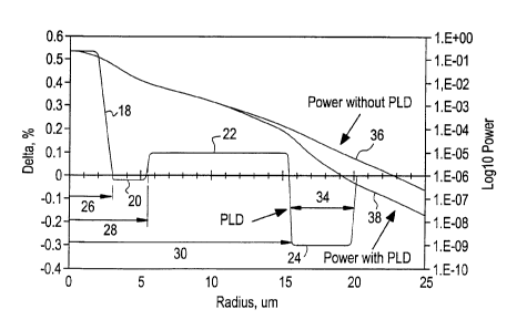
preferred ranges of relative indexes and radii. Center segment 18 has a
relative
index percent, 4°%, in the range of about 0.5% to 0.6% and outer radius
26 in
the range of about 2.0 ~m to 4.5 Vim. Center segment 18 is surrounded by first
annular segment 20 that has a relative index percent lower than that of center
segment 18, 4~%, in the range of about -0.025% to 0.01%, and outer radius 28
in the range of about 5 pm to 9 pm. First annular segment 20 is surrounded by
second annular segment 22 that has a relative index percent, DZ%, in the range
of about 0.06% to 0.30% and outer radius 30 the range of about 11 ~m to 16
~,m. The relative index percent of the PLD 24, 0P%, has a range of about -
0.05% to -0.80%, and a center radius 32 in the range of about 14 p.m to 20 wm.
The width 34 of the PLD is in the range of about 0.75 pm to 13 ~.m. Preferably
OP% is in a range of about -0.2% to -0.8%, and more preferably is more
negative than -0.25%.
Waveguide fibers have been made, using refractive index profiles within
these O% vs radius ranges, that exhibit an effective area greater than about
65
p.m2, more preferably greater than 68 pmt, and most preferably greater than 70
~m2, in combination with an attenuation at 1550 nm which is less than 0.25
CA 02380720 2002-O1-25
WO 01/11402 PCT/US00/16925
13
dB/km, preferably less than 0.23 dB/km, and more preferably less than 0.21
dB/km, a total dispersion slope, over the wavelength range 1520 nm to 1650
nm, of less than 0.09 ps/nm2-km, more preferably less than 0.08 ps/nm2-km,
and a pin array bend loss of less than 50 dB, preferably less than 35 dB, and
more preferably less than 30 dB. Microbend loss is less than about 5 dB/m and
preferably less than 3.3 dB/m. Waveguide fibers have been made using this
refractive index profile which exhibit an attenuation at 1550 nm of less than
about 0.22 dB/km. Total dispersion at 1550 nm can be made to have a positive
or negative value by placement of the zero dispersion wavelength. Cabled cut
off values are typically less than about 1500 nm.
The invention will be further illustrated by the following example that is
intended to be exemplary of the invention.
Example 2
Referring to Fig. 3, the profile shown has respective relative indexes 18,
20, 22 and 24, D°% of 0.54%, 0~ % of -0.02% , 02% of 0.1 %, PLD DP% of -
0.3%,
center segment radius 26 of 3.0 p,m, first annular segment outer radius 28 of
5.5
Vim, second annular segment outer radius 30 of 16 Vim, center radius of the
PLD
24 of 18 p,m and PLD width 34 of 4 pm.
The modeled waveguide parameters are, 1550 nm total dispersion, -
2.91 ps/nm-km, total dispersion slope, 0.077 ps/nm2-km, over the range of 1520
nm to 1650 nm, mode field diameter 9.54 pm, effective area 70.4 p,m2, fiber
cut
off wavelength 1675 nm and pin array bend loss 19 dB. Waveguide fibers
made having this index profile exhibited attenuation at 1550 nm less than 0.22
dB/km. The power distribution associated with the modeled profile is shown as
curve 38 in Fig. 2. The effect of the PLD is to significantly reduce the power
near the edge of the core region, thereby improving macrobend performance.
Comparative Example 2
A second profile was modeled corresponding to the profile of Example 2
except that the PLD was not included. In this comparative case, the modeled
CA 02380720 2002-O1-25
WO 01/11402 PCT/US00/16925
14
waveguide parameters are, 1550 nm total dispersion, -4.96 ps/nm-km, total
dispersion slope, over the range of 1520 nm to 1650 nm, of 0.068 ps/nm2-km,
mode field diameter 9.65 pm, effective area 72.4 ~m2, fiber cut off wavelength
2333 nm and pin array bend loss 31 dB. The power distribution associated with
the modeled profile is shown as curve 36 in Fig. 2. In the absence of the PLD,
power at the core edge is relatively high, a characteristic which results in
the pin
array macrobend loss being a factor of about 1.65 higher than that of the
profile
having the PLD. The respective power ratios formed by dividing power at 25 pm
from centerline by power at 10 ~m from centerline, taken from respective power
curves 38 and 36, are 1.4 x 10⁻⁵ and 1.6 x 10⁻⁴, an improvement of about an
order of magnitude. This improvement in macrobend loss is achieved without
adversely affecting the other waveguide properties.
The profile of Fig. 5 represents a group of profiles that produce the
desired properties set forth in Example 3 below. This group of profiles
generally
has a central region of the core that includes four segments surrounded by a
PLD. The design is preferred for undersea applications. Here again the
profiles
of the respective core segments may take any of the shapes set forth above in
the discussion of Fig. 2, and preferably the various segments fall within the
following preferred ranges of relative indexes and radii. Center segment 60
has
a relative index percent, 0°%, in the range of about 0.53% to 0.65% and
outer
radius 71 in the range of about 2.0 pm to 2.5 Vim. Center segment 60 is
surrounded by first annular segment 62 that has a relative index percent lower
than that of center segment 60, 4~ %, preferably in the range of about 0 to
0.065%. The outer radius 72 of segment 62 is determined by the outer radius
74 and width 80 of second annular segment 64. First annular segment 62 is
surrounded by second annular segment 64 that has a relative index percent,
02%, in the range of about 0.10% to 0.70% and center radius 73 in the range of
about 8.8 ~m to 11.8 ~m and width 80 in the range of about 0.30 pm to 9.0 pm.
Third annular segment 66 surrounds second annular segment 64 and has a
relative index in the range of about 0 to 0.05% and an outer radius 75 in the
range of about 14.5 pm to 16.5 Vim. The relative index percent of the PLD 68,
CA 02380720 2002-O1-25
WO 01/11402 PCT/US00/16925
OP%, has a range of about -0.05% to -0.80%, an inner radius 75 in the range of
12 ~m to 19.5 ~m and an outer radius 77 in the range of 17 pm to 25 p.m. The
maximum width of the PLD is therefore 13 ~,m. A preferred range of PLD width
is from 3 to 10 Vim, although PLD width can take on values in the range of
about
5 0.75 ~m to 13 pm. Relative index percent Op% is in a range of about -0.2% to
-
0.8%, and more preferably is more negative than -0.20%.
In another embodiment, the profile of Fig. 5 represents a group of profiles
that produce the desired properties set forth in Example 3 below. This group
of
profiles generally has a central core region which includes four segments
10 surrounded by a PLD. The design is particularly suited to undersea
applications. Here again the profiles of the respective core segments may take
any of the shapes set forth above in the discussion of Fig. 2, and preferably
the
various segments fall within the following preferred ranges of relative
indexes
and radii. Center segment 60 has a relative index percent, D°%, in the
range of
15 about 0.5% to 0.6% and outer radius 71 in the range of about 2.4 ~m to 3.0
Vim.
Center segment 60 is surrounded by first annular segment 62 that has a
relative
index percent lower than that of center segment 60, 0~%, in the range of about
0 to 0.1 %, and outer radius 72 in the range of about 8.4 ~m to 9.7 pm. First
annular segment 62 is surrounded by second annular segment 64 that has a
relative index percent, 42%, in the range of about 0.20% to 0.30% and outer
radius 74 the range of about 10.3 pm to 12.6 pm. Third annular segment 66
surrounds second annular segment 64 and has a relative index in the range of
about 0 to 0.05 and an outer radius 75 in the range of about 14.5 p,m to 16.5
Vim. The relative index percent of the PLD 68, OP%, has a range of about -
0.05% to -0.80%, and a center radius 78 in the range of about 16.5 pm to 20.2
Vim. The width 70 of the PLD in this embodiment is in the range of about 6.4
pm to 7.9 Vim, although as is stated above, the PLD width can have values in
the range of about 0.75 pm to 13 ~,m. Preferably ~p% is preferably in a range
of about -0.2% to -0.8%, and more preferably is more negative than -0.20%.
CA 02380720 2002-O1-25
WO 01/11402 PCT/US00/16925
16
Example 3
Referring to Fig. 5, the profile shown has respective relative indexes 60,
62, 64 and 66, 4°% of 0.55%, 4~ % of 0.01 %, 02% of 0.225%, 03% of 0,
PLD
4P% of -0.25%, center segment outer radius 71 of 2.37 ~,m, first annular
segment outer radius 72 of 8.8 Vim, second annular segment outer radius 74 of
11.4 Vim, third annular segment 66 outer radius of 15 pm, center radius of the
PLD 78 of 18.3 pm and PLD width 70 of 7.1 Vim.
Waveguide fibers made in accordance with this profile exhibit 1560 nm
total dispersion of -2.4 ps/nm-km, total dispersion slope of 0.079 ps/nm2-km,
mode field diameter of 9.36 Vim, effective area of 67.4 ~m2, cabled cut off
wavelength of 1378 nm and pin array bend loss of 29.6 dB. Using the profile
described, fibers having attenuation at 1550 nm less than 0.22 dB/km have
been made and typical 1550 nm attenuation is 0.204 dB/km. Microbend loss
for this exemplary case is about 3.32 dB/m.
In any of the embodiments set forth above, microbend loss can be
significantly reduced, typically to values less than about 1 dB/m, when a
larger
diameter polymer coating is used in combination with any of the embodiments
disclosed and described hereinabove. An embodiment of the larger diameter
coating is one in which a dual layer coating is used on a waveguide fiber
having
a diameter of 125 Vim. The primary or first layer has a diameter of 190 pm +/-
10 p,m and the secondary layer has a diameter of 285 ~m +/- 10 pm. The upper
limit on coating outside diameter is set by practical considerations such as
cost
and ease of cabling. A reasonable upper limit on coating diameter is about 310
pm for a 125 pm glass fiber diameter. Microbend loss can be improved by
using a coating having a secondary layer diameter targeted as low as 260 ~m
+/- 10 Vim. A typical fiber optic polymer coating is a dual layer urethane
acrylate based material, having ,: modulus less than 1.0 MPa for the primary
layer and a modulus greater than 650 MPa for the secondary layer. In one
embodiment the primary layer has modulus in the range of about 1.0 MPa to 1.3
CA 02380720 2002-O1-25
WO 01/11402 PCT/US00/16925
17
MPa and the secondary layer has modulus in the range of about 650 MPa to
850 Mpa.
Example 4
A waveguide fiber having parameters in accordance with those of
example 3 and a polymer coating surrounding the clad layer having a larger
diameter as set forth immediately above was made and measured. The
measured parameters were, 1560 nm total dispersion, -2.3 ps/nm-km, total
dispersion slope, 0.078 ps/nm2-km, mode field diameter, 9.25 ~,m, effective
area
66 ~m2, cabled cut off wavelength 1435 nm, pin array bend loss 4.7 dB,
attenuation at 1550 nm 0.196, and microbend loss 0.64 dB/m.
The invention as set forth in this specification may be applied to
essentially any refractive index profile to achieve improved bend resistance
without substantially changing the other waveguide fiber properties. Curve 58
in
Fig. 4 illustrates the change in 25 ~m to 10 ~m power ratio as the PLD area is
increased. Curve 58 is a best fit to a series of points generated using
different
index profiles. For lower PLD values, those less than about 1, the spread of
power ratio data points about the fitted line is 7 x 10⁻⁵. At higher PLD
areas, the
spread in power ratio is about 2.2 x 10⁻⁵. As the PLD area increases the
improvement in macrobend loss becomes less dependent upon the details of
the core segments that are inside the PLD segment. The benefits of the
invention are available for a large number of profiles that are designed for
use in
the 1250 nm to 1700 nm wavelength band.
It will be apparent to those skilled in the art that various modifications and
variations of the present invention can be made without departing from the
spirit
and scope of the invention. Thus, it is intended that the present invention
include the modifications and variations of this invention provided they come
within the scope of the appended claims and their equivalents.