Note: Descriptions are shown in the official language in which they were submitted.
CA 02380923 2002-01-31
WO 01/10025 PCT/US00/21066
METHOD AND APPARATUS FOR A MULTIPLE BAND
VOLTAGE CONTRO~LGD OSCILLATOR WITH NOISE
IMMUNITY
BACKGROUND OF THE INVENTION
1. Field of the Invention
The present invention relates to electronic circuits. More particularly, the
present invention relates to a novel and improved band switched Voltage
Controlled Oscillator (VCO) with noise immunity.
II. Description of the Related Art
Wireless communication systems rely on the predictable performance of
over the air Radio Frequency (RF) links. Wireless phone systems are required
to simultaneously monitor and control numerous RF links.
A mobile unit or wireless phone integrates numerous complex circuits.
An RF transceiver is used to provide the wireless communication link with base
stations. The RF transceiver is comprised of a receiver and a transmitter. The
receiver receives the RF transmission from the base station via an antenna
interfaced to the mobile unit. The receiver amplifies, filters, and
downconverts
the received signal to baseband signal. The baseband signal is then routed to
a
baseband processing circuit. The baseband processing circuit demodulates the
signal and conditions it for broadcast through a speaker to the user.
User input via keypad presses or voice input to a microphone is
conditioned in the baseband processing circuit. The signal is modulated and
routed to the transmitter. The transmitter takes baseband signals generated at
the mobile unit and upconverts, filters, and amplifies the signal. The
upconverted RF signal is transmitted to the base station through the same
antenna as used for the receiver.
Frequency synthesizers are used to generate the local oscillator signals
required to perform the downconversion in the receiver and the upconversion
in the transmitter. Frequency synthesis is used to generate the local
oscillator
signal because of the synthesizer's frequency stability, the spectral purity
of the
resultant signal, and the ability for digital control.
Frequency synthesizers are classified as direct or indirect. In Direct
Digital Synthesis logic circuits generate a digital representation of the
desired
signal and a D/A converter is used to convert the digital representation into
an
CA 02380923 2002-01-31
WO 01/10025 PCT/US00/21066
2
analog waveform. One common way of implementing DDS is to store a table
of waveform phases in memory. Then the rate at which the phases are clocked
out of memory is directly proportional to the frequency of the output signal.
While DDS can generate an extremely accurate representation of a sine wave,
the output frequency is limited by the clocking rate.
Indirect synthesis utilizes a phase lock loop locked to the output of an
oscillator. Indirect frequency synthesis is more popular for high frequency
designs because the output of a high frequency oscillator can be divided down
to a frequency within the operating range of the phase lock loop.
FIG. 1 shows a block diagram of an indirect frequency synthesizer
utilizing a phase lock loop. A VCO 110 capable of tuning over the desired
frequency range is used to provide the LO output 112. The output of the VCO
110 is also sent to the input of a frequency divider circuit 120, denoted =N
where N represents the divider ratio. The divided output is provided as a
first
input to a phase detector 130. A second input to the phase detector 130 is the
output of a reference oscillator 140. The phase lock loop operates to tune the
output of the VCO 110 such that the output of the frequency divider 120 is
identical to the output of the reference oscillator 140. The phase detector
130
provides an output signal corresponding to a phase error between the two
input signals. The phase detector 130 output is conditioned through a Low
Pass Filter (LPF) before it is provided to the frequency control input of the
VCO
110. Thus, the VCO 110 is controlled to maintain phase lock with the reference
oscillator 140. It can be readily deduced from the block diagram that
incrementing or decrementing the value of the divider ratio N results in a
frequency change in the LO output 112 equal to the reference oscillator 140
frequency. The frequency of the reference oscillator 140 determines the
frequency step size of the LO.
Frequency variations in the VCO 110 output can only be corrected by the
phase lock loop if the rate of the frequency variations is less than the loop
bandwidth. The phase lock loop is unable to correct for VCO frequency
variations that occur at a rate higher than the loop bandwidth. The settling
time of the phase lock loop will depend on the initial frequency offset and
the
loop bandwidth. A wider loop bandwidth results in a faster settling time. A
VCO with good noise immunity will reduce frequency variations thereby
reducing the settling time of the phase lock loop. Therefore, it is important
to
design a VCO with good noise immunity while maintaining the frequency
tuning characteristics.
A VCO is merely a tunable oscillator. A typical oscillator circuit is
comprised of an amplifier and a resonant circuit, commonly referred as a
CA 02380923 2002-01-31
WO 01/10025 PCT/US00/21066
3
resonant circuit. The resulting oscillator has a frequency output where the
gain
is greater thait unity and the phase is equal to zero. The resonant circuit
sets
this frequency of oscillation. The relationship is most easily seen on a Bode
diagram. FIG. 2A illustrates a Bode diagram for a typical oscillator. Curve
210
is representative of the gain in decibels of the oscillator as referenced to
the left
vertical axis and Curve 220 is representative of the phase in degrees as
referenced to the right vertical axis. As indicated by Point 230, the
oscillation
occurs when the oscillator gain is approximately 14 dB and the phase is zero
producing an oscillation at approximately 124 MHz.
To create a VCO the resonant circuit is comprised of at least one variable
component wherein the reactance of the variable component is a function of a
control signal, typically a voltage level, so that the frequency of zero
phase, and
consequently the frequency of oscillation, is also variable. When the VCO is
required to tune over a large frequency range the variable component must be
capable of tuning the resonant circuit over the large frequency range.
Possible
circuit implementations for a variable resonant circuit capable of covering a
large frequency range include a resonant circuit incorporating a highly
sensitive variable component or a resonant circuit requiring an extended
control voltage range. The first alternative presents some problems because
the
VCO gain, measured in terms of MHz/Volt, becomes very high. This results in
large frequency changes for relatively small control voltage changes and makes
the VCO more susceptible to noise induced on the tuning line. The second
alternative also has disadvantages since the required control voltage range is
very large. Large control voltages can present a problem in mobile battery
powered electronics having limited available supply voltage ranges.
A third alternative to designing a VCO to cover a wide tuning range can
be implemented in applications where distinct frequency bands must be
supported. This situation occurs commonly in the design of a dual band
wireless phone. Wireless phones most commonly operate in the cellular band
(Transmit band 824-849MHz, Receive band 869-894MHz) and the Personal
Communication System (PCS) band (Transmit band 1850-1910MHz, Receive
band 1930-1990MHz). A single phone can be designed to operate in both
cellular and PCS bands. The frequency plan within the phone is typically
designed to minimize the number of oscillators thereby minimizing the cost of
the phone. However, even the most judicious frequency plan requires different
LO frequencies when operating in one band over the other. In order to support
both the cellular and PCS operating bands, components are selectively switched
in the resonant circuit of the oscillator. Components are included in the
resonant circuit of an oscillator and switched using diode switches. The
CA 02380923 2002-01-31
WO 01/10025 PCT/US00/21066
4
circuit's operating frequency limits the particular type of diode used for the
switch. When the switch is in the closed position the diode must be capable of
carrying varying RF currents while maintaining a minimal resistance. When
the switch is in the open position the diode must be capable of isolating the
RF
voltages and maintaining a high resistance. A PIN diode switch is commonly
used at RF frequencies for a switch although other types of diodes may be used
as a switch. Additionally, the circuit is not limited to the use of a diode
switch.
Any switch that is capable of carrying RF currents in the closed position and
is
capable of RF isolation in the open position can be implemented within the
circuit.
When the diode switch is forward biased the switched component
becomes active within the resonant circuit. When the diode switch is not
forward biased, the component does not contribute electrically to the resonant
circuit. Switching a component in the resonant circuit greatly extends the
tuning range of the oscillator without a corresponding increase in the VCO
gain.
It is not sufficient that the resonant circuit tune the oscillator to the
desired operating frequency. The Q of the resonant circuit is important in
maintaining a specific output frequency at a given control voltage level. FIG.
2B depicts the phase response of two resonant circuits having different Q
values. A lower circuit Q generates a more gentle phase response, whereas a
higher circuit Q generates a sharper phase response. A higher circuit Q is
desired to minimize the effects of small phase variations on output frequency.
The phase response of a circuit having a relatively low circuit Q is shown in
curve 240. Curve 250 illustrates a circuit having a higher circuit Q. It can
be
seen for a given phase variation the change in frequency is more pronounced in
the circuit having the lower circuit Q. The magnitude of f2, the frequency
change in a low Q circuit for a given phase variation, is greater than the
magnitude of f1, the frequency change in a high Q circuit for the same phase
variation.
Application specific integrated circuits are available that integrate many
wireless phone functions into a single IC. Frequency synthesizer IC's are
available that integrate nearly all of the required synthesizer circuits onto
one
chip. Typically, the user of one of these IC's only needs to provide a
resonant
circuit, loop filter, and reference oscillator in addition to the IC in order
to
produce a synthesized LO. The remaining elements of the synthesizer, the
amplifier portion of the VCO, the frequency divider, and the phase detector
are
integrated onto one IC. The user provides the resonant circuit required
CA 02380923 2002-01-31
WO 01/10025 PCT/US00/21066
generating the desired output frequency. The user also provides the low pass
filter design generating the desired loop banciwidth.
Although application specific IC's simplify the implementation of the LO
in a wireless phone, the wireless phone operating environment presents
5 additional noise sources which must be considered. Cost and space
limitations
in a wireless phone further constrain available noise filtering solutions.
The mobile phone design differs greatly depending on the particular
mobile system it is supporting. Specifications outlining mobile phone design
include Telecommunications Industry Association (TIA) /Electronic Industries
Association (EIA) IS-95-B MOBILE STATION-BASE STATION
COMPATABILITY STANDARD FOR DUAL-MODE SPREAD SPECTRUM
SYSTEMS as well as TIA/EIA IS-98-B, RECOMMENDED MINIMUM
PERFORMANCE STANDARDS FOR DUAL-MODE SPREAD SPECTRUM
CELLULAR MOBILE STATIONS. The specification covering the operation of a
CDMA system in the Personal Communication Systems (PCS) band is the
American National Standards Institute (ANSI) J-STD-008 PERSONAL
STATION-BASE STATION COMPATIBILITY REQUIREMENTS FOR 1.8 TO
2.0 GHZ CODE DIVISION MULTIPLE ACCESS (CDMA) PERSONAL
COMMUNICATIONS SYSTEMS. Similarly, the phone, or personal station, is
specified in ANSI J-STD-018, RECOMMENDED MINIMUM PERFORMANCE
REQUIREMENTS FOR 1.8 TO 2.0 GHZ CODE DIVISION MULTIPLE ACCESS
(CDMA) PERSONAL STATIONS. Additionally, the mobile phone specification
defines features which, when implemented in phone hardware, tend to increase
sources of noise within the phone.
One beneficial feature that is utilized in CDMA phone systems such as
those specified in IS-95 and J-STD-008 is multiple data rate sets. In order to
take
advantage of the variable nature of a wireless phone communication link, the
CDMA specifications provide for data transmission at reduced rates. When a
person is engaged in a telephone conversation there are numerous periods in
which only one party will be speaking. During periods of reduced speech
activity the telephone can reduce the data rate of the transmission resulting
in a
lower average transmit power level.
The communication link from the wireless phone back to the base station
is termed the reverse link. On the reverse link, reduction in average transmit
power is accomplished by turning off the transmitter for a fraction of the
time
during periods when activity is low. In a CDMA reverse link the phone always
transmits at the full data rate however, when the internal structure allows
operation at a reduced data rate the data is repeated a number of times. As an
example, when the phone is able to operate at one-half of the full data rate
the
CA 02380923 2002-01-31
WO 01/10025 PCT/US00/21066
6
information is repeated twice to bring the transmitted data rate up to the
full
data rate. Similarly, one-fourth rate &ta is repeated four times to achieve a
full
data rate.
To conserve power on the reverse link, each 20mS data frame is
subdivided into sixteen 1.25mS time groupings. When the phone is operating
at a full data rate all sixteen of the groups within the frame are
transmitted.
However, when the phone is operating at a reduced data rate only a fraction of
the sixteen groups is transmitted. The fraction of groups transmitted is equal
to
the reduction in the data rate. When the phone operates at one-half the full
data rate one-half of the groups is transmitted. However, note that no data is
lost since data is repeated in inverse proportion to the data rate reduction.
One-half rate data is repeated twice but only half of the data is transmitted.
The redundant portion of the data is not transmitted. Similarly, one-eighth
rate
data is repeated eight times but only one-eighth of the data is transmitted.
When the phone operates at a reduced data rate, power is gated to select
active circuits on the transmit path. The power to the circuits is gated off
when
the data is not being transmitted. The power is gated back on to the circuits
prior to transmitting the desired data group. Power gating serves to conserve
power within the wireless phone. This results in a much desired extended
battery life.
An adverse effect of power gating is the sudden load changes applied to
the phone power supply. The portions of the RF transmit path that are
switched on and off present the greatest loads on the power supply. Therefore,
during power gating, the phone power supply is subjected to the greatest load
variations that it will experience. Since no power supply is insensitive to
load
variations the output of the power supply will exhibit voltage ripple at the
rate
that power gating occurs. The actual voltage ripple on the supply voltage
lines
is a function of the power supply load rejection, the rate of power gating,
and
the change in power supply load due to power gating. The change in power
supply load varies in relation to the RF communication link the phone is
maintaining with the base station. The change in load current will be greater
when the phone is transmitting at a higher RF power level than when the
phone is transmitting at a decreased RF power level. The power gating may
occur at each 1.25 mS time grouping used for each data frame on the reverse
link. This results in a power supply load variation with a significant 800 Hz
frequency component.
What is desired is a voltage controlled oscillator design that maintains a
stable output frequency with a constant control voltage applied. The VCO
must be able to be switched such that it is tunable over two distinct
frequency
CA 02380923 2002-01-31
WO 01/10025 PCT/US00/21066
7
bands. Moreover, the VCO output must be insensitive to power supply noise.
Specifically, when the VCO is implemented in a CDMA phone the VCO output
must be insensitive to power supply noise created by power gating the RF
transmit path. Another object of the invention is the design of a high Q, low
cost, low component count, component switched, noise insensitive circuit for
use as a resonant circuit within a VCO.
SUMMARY OF THE INVENTION
The present invention is a novel and improved multiple band Voltage
Controlled Oscillator (VCO) having increased noise immunity. Additionally,
the invention may be viewed as a novel resonant circuit configuration that
contains switched components, has high Q, and is insensitive to noise. The
novel resonant circuit can be implemented with an amplifier or application
specific integrated circuit to generate a VCO having the characteristics of
multiple band coverage, noise insensitivity, and frequency stability.
In a first embodiment all of the elements of the resonant circuit are
connected in a balanced configuration with the exception of the inductor.
First
and second coupling capacitors comprise the positive and negative balanced
connections to the resonant circuit. The outputs of the first and second
coupling capacitors are interconnected using an inductor in series with a
switched capacitor. A first tuning capacitor connects the output of the first
coupling capacitor to a first variable capacitor. A second tuning capacitor
connects the output of the second coupling capacitor to a second variable
capacitor. The opposite ends of the first and second variable capacitors are
connected together thereby maintaining a balanced configuration with respect
to the balanced connections of the resonant circuit. A diode switch is
connected
in parallel with the switched capacitor such that the switched capacitor is
electrically connected to the resonant circuit when the diode switch is not
forward biased. The switched capacitor is not electrically connected to the
resonant circuit when the diode switch is forward biased.
In the first embodiment the first and second tuning capacitors are
utilized as a voltage controlled variable circuit. In the first embodiment the
capacitance value of the variable circuit is changed with the application of a
control voltage. Any type of variable circuit whose impedance changes
according to an applied voltage can be used in a resonant circuit to enable
the
resonant frequency to be tuned using a control voltage. The preferred
embodiments described in the present invention utilize variable capacitors as
the variable circuit.
CA 02380923 2002-01-31
WO 01/10025 PCT/US00/21066
8
Operation of the switch causes the center frequency of the VCO to shift
between two values, fl anu f2. More particularly, actuation of the switch
cau5es
the resonant frequency of the resonant circuit to vary, thereby shifting the
center frequency of the VCO between fl and f,.
The first embodiment has the advantage of a maximized circuit Q. This
is because only one inductor is utilized in the circuit. Inductor Q is the
limitation to achieving high circuit Q. The elimination of the majority of
inductors in the circuit maximizes the circuit Q. However, the circuit is not
as
noise insensitive as the second embodiment.
In a second embodiment all of the elements of the resonant circuit are
connected in a balanced configuration. First and second coupling capacitors
comprise the positive and negative balanced connections to the resonant
circuit,
just as in the first embodiment. The outputs of the first and second coupling
capacitors are connected to first and second inductors. The first and second
inductors are each connected to one of the coupling capacitors and ground. A
first tuning capacitor connects the output of the first coupling capacitor to
a
first variable capacitor. A second tuning capacitor connects the output of the
second coupling capacitor to a second variable capacitor. The opposite ends of
the first and second variable capacitors are connected together thereby
maintaining a balanced configuration with respect to the balanced connections
of the resonant circuit. The second embodiment, as presently described, is
completely balanced with respect to the input of the resonant circuit. One end
of the switched capacitor is connected to the output of the second coupling
capacitor. The switched capacitor is connected in series to the diode switch
that
is then connected to the output of the first coupling capacitor. The output of
the first coupling capacitor is connected to the output of the second coupling
capacitor using the switched capacitor in series with the diode switch. The
resonant circuit is indifferent to whether the switched capacitor is connected
to
the output of the first coupling capacitor with the diode switch connected to
the
output of the second coupling capacitor or if the positions of the switched
capacitor and diode switch are transposed.
Operating the switch causes the center frequency of the VCO to shift
between two values, fl and f,. More particularly, actuation of the switch
causes
the capacitance associated with resonant circuit to vary, thereby shifting the
resonant frequency of the resonant circuit and thus changing the center
frequency of the VCO from f, to f,
The second embodiment also has greater noise immunity due to an
additional pole in high pass filter. When viewed from the inputs each of the
balanced inputs has effectively a high pass filter configuration. This is due
to
CA 02380923 2007-05-14
74769-496
9
the configuration of the coupling capacitors in relation to
the inductors. This high pass filter effectively acts to
remove the majority of noise induced onto the resonant
circuit. The noise is eliminated from affecting the
variable capacitors thereby eliminating the effects of
induced noise on the operation of the resonant circuit.
According to an aspect of the present invention,
there is provided a Voltage Controlled Oscillator (VCO) in a
wireless phone system comprising: an ampiifier; and a
resonant circuit connected to the amplifier for tuning the
oscillator to a desired operating frequency, said resonant
circuit comprising: a variable circuit whose impedance is
determined by a control voltage set to a first state for a
first data rate for transmitted data and set to a second
state for a second data rate for transmitted data in said
wireless phone system; and a low frequency attenuating
filter between an input to the resonant circuit and the
variable circuit.
According to another aspect of the present
invention, there is provided a method for increasing the
noise immunity of a Voltage Controlled Oscillator (VCO) in a
wireless phone system comprising: implementing a resonant
circuit with a variable circuit whose impedance is
determined by a control voltage set to a first state for a
first data rate for transmitted data and set to a second
state for a second data rate for transmitted data in said
wireless phone system and a low frequency attenuating filter
between an input to the resonant circuit and the variable
circuit; and connecting the resonant circuit to an
amplifier.
According to yet another aspect of the present
invention, there is provided a multiple band resonant
CA 02380923 2007-05-14
74769-496
9a
circuit in a wireless phone system capable of tuning across
a range of resonant frequencies within each band comprising:
an inductor; a switched capacitor connected in series with
the inductor; a variable circuit whose impedance is
determined by a control voltage set to a first state for a
first data rate for transmitted data and set to a second
state for a second data rate for transmitted data in said
wireless phone system; a first tuning capacitor connecting a
first end of the series combination of the inductor and the
switched capacitor to a first end of the variable circuit; a
second tuning capacitor connecting a second end of the
series combination of the inductor and switched capacitor to
a second end of the variable circuit; a first coupling
capacitor connected to the junction of the first tuning
capacitor and the inductor; a second coupling capacitor
connected to the junction of the second tuning capacitor and
the switched capacitor; and a switch connected in parallel
to the switched capacitor to selectively provide a short
circuit connection across the switched capacitor thereby
electrically removing the switched capacitor from the
resonant circuit.
According to still another aspect of the present
invention, there is provided a multiple band resonant
circuit in a wireless phone system capable of tuning across
a range of resonant frequencies within each band comprising:
an inductor; a first coupling capacitor connected to a first
end of the inductor; a second coupling capacitor connected
to a second end of the inductor; a switched capacitor; a
switch connected in series with the switched capacitor,
whereby the series combination of the switch and the
switched capacitor is connected in parallel to the inductor;
a variable circuit whose impedance is determined by a
control voltage set to a first state for a first data rate
CA 02380923 2007-05-14
74769-496
9b
for transmitted data and set to a second state for a second
data rate for transmitted data in said wireless phone
system; a first tuning capacitor connecting the first end of
the inductor to a first end of the variable circuit; and a
second tuning capacitor connecting the second end of the
inductor to a second end of the variable circuit; wherein
the switched capacitor contributes to the resonant frequency
of the resonant circuit when the switch is enabled and the
switched capacitor does not contribute to the resonant
frequency of the resonant circuit when the switch is
disabled.
CA 02380923 2007-05-14
74769-496
9c
BRIEF DESCRIPTION OF THE DRAWINGS
The features, objects, and advantages of the present invention will
become more apparent from the detailed description set forth below when
taken in conjunction with the drawings in which like reference characters
identify correspondingly throughout and wherein:
FIG. 1 is a block diagram of a synthesized local oscillator;
FIG.s 2A-2B are amplitude and phase plots characterizing oscillator
circuits;
FIG. 3 is a block diagram of an integrated circuit synthesized oscillator;
FIG. 4 is a block diagram showing the first embodiment of the invention
incorporated with an integrated circuit oscillator; and
FIG. 5 is a block diagram showing the second embodiment of the
invention incorporated with an integrated circuit oscillator.
DETAILED DESCRIPTION OF THE PREFERRED
EMBODIMENTS
FIG. 3 illustrates a block diagram of a typical local oscillator
implementation used in a wireless phone. A synthesized oscillator IC 300
incorporates a Phase Lock Loop (PLL) 302 as well as an amplifier configured as
an osciIlator 304. The synthesized oscillator IC 300 requires an external
resonant circuit and loop filter 310 in order to operate. The oscillator 304
is
configured as a Voltage Controlled Oscillator (VCO) if the resonant circuit
can
be tuned by the application of a control voltage.
The resonant circuit is comprised of an inductor 320 in parallel with a
capacitive network. The capacitive network utilizes first and second variable
capacitors, 342 and 344 respectively, connected in series. The first variable
capacitor 342 is connected to a first side of the inductor 320 through a first
tuning capacitor 332. The second variable capacitor 344 is connected to the
second side of the inductor 320 through a second tuning capacitor 334. The
point where the first variable capacitor 342 connects to the second variable
capacitor 344 is tied to signal ground.
CA 02380923 2002-01-31
WO 01/10025 PCT/US00/21066
The oscillator 304 within the synthesized oscillator IC 300 operates at the
frequency of the resonant circuit. A sample of the output of the oscillator
304 is
routed to the PLL 302. The PLL 302 compares the phase of the oscillator 304
output signal against a reference signal (not shown). The resultant error
signal
5 is passed through a loop filter 310 then is applied to the resonant circuit.
The
output of the loop filter 310 is applied to the variable capacitors, 342 and
344,
through first and second bias resistors, 352 and 354. A first bias resistor
352
connects the output of the loop filter 310 to the terminal of the first
variable
capacitor 342 that is connected to the first tuning capacitor 332. Similarly,
a
10 second bias resistor 354 is used to connect the output of the loop filter
310 to the
terminal of the second variable capacitor 344 that is connected to the second
tuning capacitor 334. The first variable capacitor 342 and the second variable
capacitor 344 may be implemented as varactor diodes. The output of the loop
filter 310 is used to reverse bias the varactor diodes. The varactor diodes
change their capacitance values based on the level of reverse bias applied.
Therefore, by controlling the varactor diode reverse bias voltage the
frequency
of the oscillator can be controlled. The control voltage is varied to maintain
phase lock within the PLL 302.
When a wireless phone LO is configured as shown in FIG. 3 the
oscillator 304 can only tune over the range of the resonant circuit. If the
oscillator 304 is required to tune over a large frequency span such that the
phone can cover multiple frequency bands, the resonant circuit must be capable
of tuning over the entire range. Tuning the resonant circuit of FIG. 3 over a
wide range can be accomplished in two ways.
A first method utilizes highly sensitive variable capacitors, 342 and 344.
The control voltage range is maintained at a minimum value when highly
sensitive variable capacitors are used. However, the sensitivity of the
variable
capacitors makes the resonant circuit sensitive to noise induced on the
circuit.
Any source of noise induced on the variable capacitor bias causes a shift in
the
resonant frequency of the circuit. If the rate of induced noise is higher than
the
loop bandwidth the PLL 302 is unable to correct the error.
A second method utilizes low sensitivity variable capacitors with an
extended control voltage range. However, the extended control voltage range
presents a problem for wireless phones operating off of battery power. Since
the voltage provided by batteries is relatively low, the expansion of the
control
voltage range requires a step up of the available voltage. A voltage step up
is
accomplished with a DC-DC converter. A DC-DC converter does not operate
at 100% efficiency. The loss in the step up voltage conversion is wasted
battery
power. Minimizing battery power consumption is a major priority in wireless
CA 02380923 2002-01-31
WO 01/10025 PCT/US00/21066
11
phones. Another major priority in wireless phones is minimizing physical size.
Both of these high priority design constraints discourage the use of extended
control voltage ranges in a wireless phone.
An alternative resonant circuit configuration integrates switched
components into the resonant circuit. The components are switched out of the
resonant circuit for operation in a first frequency band and the components
are
switched into the resonant circuit for operation in a second frequency band.
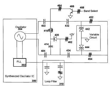
The first embodiment of the present invention is illustrated in FIG. 4.
The LO configuration utilizes the same synthesized oscillator IC 300 and loop
filter 310 described in FIG. 3. However, the configuration of the resonant
circuit in FIG. 4 differs from that shown in FIG. 3. The resonant circuit
shown
in FIG. 4 includes a switched capacitor 414 that can be switched into and out
of
the circuit according to the bias across the diode switch 420. However, the
resonant circuit shown in FIG. 4 contains additional elements not incorporated
in the resonant circuit of FIG. 3.
The resonant circuit shown in FIG. 4 incorporates first and second
coupling capacitors, 402 and 404. These coupling capacitors will decrease the
level of any noise from the Oscillator pins to the resonant circuit. The first
terminal of each coupling capacitor is used to connect the resonant circuit to
the
respective terminal of the oscillator 304. The second terminal of each
coupling
capacitor, 402 and 404, is connected to opposite ends of the remainder of the
resonant circuit. The second terminal of the first coupling capacitor 402 is
connected to an inductor 410 placed in series with a switched capacitor 414.
The end of the switched capacitor 414 that is not connected to the inductor is
connected to the second terminal of the second coupling capacitor 404.
A diode switch 420 is connected in parallel with the switched capacitor
414. The anode of the diode switch 420 is connected to the second terminal of
the second coupling capacitor 404 and the cathode of the diode switch 420 is
connected to the junction of the inductor 410 and the switched capacitor 414.
The anode of the diode switch 420 is pulled up to the supply voltage rail
using
a pull up resistor 462. At the junction of the first coupling capacitor 402
and the
inductor 410 is a circuit used to control the forward bias on the diode switch
420. This circuit is comprised of a pull down resistor 464 connected to a DC
switch 466. When the DC switch 466 is closed the pull down resistor 464
provides a DC path from the inductor 410 to ground. When the DC switch 466
is open, the pull down resistor 464 is open circuited and no current flows
through it. A Band Select signal driving a control resistor 468 connected to
the
DC switch 466 controls the DC switch 466. The actual configuration of the
switch placed in parallel with the switched capacitor 414 is not critical. The
CA 02380923 2002-01-31
WO 01/10025 PCTIUSOO/21066
12
forward biased diode switch 420 shown in FIG. 4 is illustrative only and is
not a
limitation on the switch configuration that can be used in the resonant
circuit.
Any comparable switch placed in parallel with the switched capacitor 414 is
allowable.
The remainder of the FIG. 4 resonant circuit is configured much like that
shown in FIG. 3. A first tuning capacitor 432 connects the second terminal of
the first coupling capacitor 402 to a first variable capacitor 442. A second
tuning capacitor 434 connects the second terminal of the second coupling
capacitor 404 to a second variable capacitor 444. The ends of the two variable
capacitors, 442 and 444, opposite the tuning capacitors, 432 and 434, are
connected together and tied to ground. The control voltage signal out of the
loop filter 310 is applied to each of the variable capacitors, 442 and 444,
through
bias resistors 452 and 454. A first bias resistor 452 connects the control
voltage
signal out of the loop filter 310 to the junction of the first variable
capacitor 442
and first tuning capacitor 432. A second bias resistor 454 connects the
control
voltage signal out of the loop filter 310 to the junction of the second
variable
capacitor 444 and second tuning capacitor 434. The bias resistors 452 and 454
apply the control voltage signal to reverse bias the variable capacitors when
the
variable capacitors 442 and 444 are implemented as varactor diodes. In present
embodiment, the control voltage may be varied from 0 - 3 Volts. The control
voltage signal is used to adjust the present invention for variations in
components and variations due to temperature.
The ability to frequency band switch the first embodiment is described
as follows. When the DC switch 466 is closed the diode switch 420 is forward
biased and conducts. When the diode switch 420 conducts, the switched
capacitor 414 is short circuited and does not electrically contribute to the
resonant circuit. The resonant frequency fl is then determined by the value of
the inductor in parallel with the capacitive tuning circuit comprised of the
tuning capacitors, 432 and 434, in conjunction with the variable capacitors
442
and 444. When the Band Select signal controls the DC switch 466 to an open
circuit condition the diode switch 420 no longer conducts.
The switched capacitor 414 is electrically connected to the resonant
circuit when the diode switch 420 is not conducting. The resonant frequency f2
of the circuit is increased when the switched capacitor 414 electrically
contributes to the resonant circuit. The resonant frequency f, is increased
because the switched capacitor 414 appears in series with the inductor 410.
The
series combination results in a reactance that is the sum of each reactance.
Since
the reactance of an inductor is opposite the reactance of a capacitor the
effect of
a series combination is a reactance that is less than the larger of the two
CA 02380923 2002-01-31
WO 01/10025 PCT/US00/21066
13
reactances. The reactance of the switched capacitor 414 is chosen to be less
than
the reactance of the inductor 410 such that the series combination of the two
elements has the reactance of an equivalently smaller inductor. A smaller
inductor in the resonant circuit increases the resonant frequency.
The first embodiment of the invention shown in FIG. 4 has several
advantages. One advantage is that the embodiment maximizes the circuit Q.
The circuit Q is maximized because the circuit is implemented with the
minimum number of inductors. Because of their physical structure, inductors
have much lower component Q and larger size than capacitors. A resonant
circuit that achieves band switching by the addition and removal of inductors
will have a lower circuit Q than a resonant circuit that achieves band
switching
by the addition and removal of capacitors. Circuit Q is also maximized by the
series combination of the inductor 410 and switched capacitor 414. The circuit
Q is higher with the series combination of the inductor 410 and switched
capacitor 414 because a larger inductor 410 value is used. Since inductor 410
component Q is determined as XL/RL a larger value of inductance provides a
higher component Q. It is also easier to center the two operating frequencies
using capacitors over inductors because capacitor values are available in
finer
gradations than inductor values.
Another advantage of the first embodiment is increased noise immunity.
When circuits on the transmit path are power gated on/off to conserve power
during reduced rate transmission in a CDMA wireless phone system, the
sudden changes in the power supply load result in fluctuations in the power
supply output. The fluctuations in the power supply output affect all active
components. The synthesized oscillator IC 300 may be affected by the power
supply fluctuations by exhibiting a corresponding voltage ripple on all output
lines. The voltage ripple will be exhibited on the terminals connecting to the
resonant circuit as well as on the control voltage line to the loop filter
310.
The two coupling capacitors, 402 and 404, help to decrease the effect of
any noise induced on the resonant circuit via the oscillator pins. The
coupling
capacitors, 402 and 404, provide additional reactances that serve to reduce
the
level of voltage ripple that ultimately reaches the variable capacitors, 442
and
444.
The band switch configuration of the resonant circuit provides increased
noise immunity by minimizing the VCO gain. The VCO gain is a measure of
the tuning sensitivity of the VCO, is denoted Kvõ and is typically measured in
MHZ/V. The band switch configuration minimizes the VCO gain by limiting
the capacitance change required of the variable capacitors in the resonant
circuit. The capacitance range is minimized because the large scale change
CA 02380923 2002-01-31
WO 01/10025 PCTIUSOO/21066
14
required to switch frequency bands is performed by the inclusion of the
switcited capacitor 414. Therefore, a limited voltage control range can
accurately control the oscillator frequency in both bands without increasing
the
value of KV. In the first embodiment, the L and C values are selected such
that
the Kv values are about the same at the operating frequencies f, and f2.
A second embodiment of the invention, shown in FIG. 5, provides a
greater level of noise immunity at a slight degradation in circuit Q. The
second
embodiment also utilizes a band switched resonant circuit configuration. The
second embodiment is very similar to the first embodiment.
The second embodiment incorporates first and second coupling
capacitors, 502 and 504, as the inputs to the resonant circuit. The
synthesized
oscillator IC 300 has a balanced pair of connections for the external resonant
circuit. A first terminal of the first coupling capacitor 502 is connected to
the
positive resonant circuit interface connection of the synthesized oscillator
IC
300. The second terminal of the first coupling capacitor is connected to a
first
inductor 512. The first inductor 512 provides a circuit path to ground.
Similarly, a first terminal of the second coupling capacitor 504 is connected
to
the negative resonant circuit interface connection of the synthesized
oscillator
IC 300. The second terminal of the second coupling capacitor 504 connects to a
second inductor 514. The second inductor 514 provides a circuit path to
ground.
A switched capacitor 522 in series with a diode switch 520 connects the
second terminal of the first coupling capacitor 502 to the second terminal of
the
second coupling capacitor 504. The anode of the diode switch 520 is connected
to the switched capacitor 522 in the series connection. FIG. 5 shows the
switched capacitor 522 connected to the second terminal of the second coupling
capacitor 504 and the cathode of the diode switch 520 connected to the second
terminal of the first coupling capacitor 502. However, the series connection
of
the switched capacitor 522 and the diode switch 520 can be reversed without
affecting operation of the circuit. That is, the cathode of the diode switch
520 is
connected to the second terminal of the second coupling capacitor 504 and the
switched capacitor 522 is connected to the second terminal of the first
coupling
capacitor 502 with no change in circuit operation.
The circuit required to bias the diode switch 520 includes a pull up
resistor 564 connected on one end to the anode of the diode switch 520 and
connected on the other end to a DC switch 566. The DC switch 566 connects the
pull up resistor 564 to the power supply rail when in the closed condition.
When the DC switch 566 is closed DC current flows follows a path to ground
through the pull up resistor 564, the forward biased diode switch 520 and the
CA 02380923 2002-01-31
WO 01/10025 PCT/USOO/21066
first inductor 512. When the DC switch 566 is in the open condition the pull
up
resistor 564 is open circuited and no current flows through the pull up
resistor
564. A Band Select signal driving a control resistor 568 connected to the
control
terminal of the DC switch 566 controls the operation of the DC switch 566.
5 The remainder of the resonant circuit is configured in the same way as in
the first embodiment. A first tuning capacitor 532 connects the second
terminal
of the first coupling capacitor 502 to a first variable capacitor 542. A
second
tuning capacitor 534 connects the second terminal of the second coupling
capacitor 504 to a second variable capacitor 544. The ends of the two variable
10 capacitors, 542 and 544, opposite the tuning capacitors, 532 and 534, are
connected together and tied to ground. The control voltage signal out of the
loop filter 310 is applied to each of the variable capacitors, 542 and 544,
through
bias resistors 552 and 554. A first bias resistor 552 connects the control
voltage
signal out of the loop filter 310 to the junction of the first variable
capacitor 542
15 and first tuning capacitor 532. A second bias resistor 554 connects the
control
voltage signal out of the loop filter 310 to the junction of the second
variable
capacitor 544 and second tuning capacitor 534. The bias resistors 552 and 554
apply the control voltage signal to reverse bias the variable capacitors when
the
variable capacitors 542 and 544 are implemented as varactor diodes. In present
embodiment, the control voltage may be varied from 0 - 3 Volts. The control
voltage signal is used to adjust the present invention for variations in
components and variations due to temperature.
The second embodiment of the invention also implements a band
switched oscillator. When the diode switch 520 is forward biased the switched
capacitor 522 is electrically connected to the resonant circuit. The switched
capacitor 522 appears in the resonant circuit in parallel with the capacitive
network comprised of the tuning capacitors, 532 and 534, and the variable
capacitors, 542 and 544. Thus, the switched capacitor 522 increases the
capacitance value in the resonant circuit. The effect is to lower the resonant
frequency of the resonant circuit to fl. When diode is off, the circuit
operates at
higher resonant frequency f2. The resonant circuit in the second embodiment
maintains a low value of Kv, the VCO gain, by providing coverage in both
oscillator frequency bands through the use of a band switched resonant
circuit.
The primary advantage of the resonant circuit of the second embodiment
is in relation to noise immunity. As in the case of the first embodiment, the
second embodiment provides greater noise immunity when compared to a
wide band oscillator not utilizing a band switched configuration. The lower
value of KV, the VCO gain, in the band switched oscillator makes the band
switched oscillator less sensitive to noise induced on the control voltage
line.
CA 02380923 2002-01-31
WO 01/10025 PCT/USOO/21066
16
Although the loop filter 310 will remove the majority of noise induced on the
control voltage line, not all of the noise will be eliminated. An equivalent
voltage ripple on the control voltage line of the wide band oscillator will
result
in a greater frequency deviation then the same voltage ripple induced on the
control voltage line of the band switched oscillator. The improvement in noise
immunity for the band switched design is the ratio of the VCO gains for the
two oscillator designs.
The fully balanced design of the resonant circuit also produces increased
immunity to noise induced at the inputs to the resonant circuit. The resonant
circuit is configured as a high pass filter when viewed from either input
terminal. The combination of a series coupling capacitor, 502 or 504, in
conjunction with either the first or second inductor, 512 or 514, in shunt
produces a two pole high pass filter. The high pass filter configuration is
particularly helpful in eliminating noise from the synthesized oscillator IC
300.
One particular source of noise from the synthesized oscillator IC 300 is
attributable to power supply voltage fluctuations corresponding to power
cycling of active devices in the transmit signal path. Power cycling of active
devices in the transmit signal path occurs when a CDMA wireless phone
operates at a reduced data rate. When the CDMA phone is operating in a
reduced data rate only one copy of a number of repeated data periods is
transmitted. This not only results in power savings in the phone but also a
reduction in the average RF power transmitted from the phone. The reduced
average phone RF transmit power results in less interference to other phones
operating in the same band. Transmit power cycling results in power supply
noise with a significant 800 Hz frequency component. The power supply noise
is induced onto the resonant circuit via the interface connections of the
synthesized oscillator IC 300. The high pass filter incorporated into the
design
of the resonant circuit eliminates the noise from the variable capacitors 542
and
544. The result is the resonant circuit is unaffected by noise induced from
the
synthesized oscillator IC 300 since no other components in the resonant
circuit
are affected by voltage variations. The output of the oscillator 304 then
exhibits
better phase noise because the resonant circuit is not affected by noise.
The invention provides an oscillator having a majority of desired
characteristics. The high Q of the resonant circuit ensures the oscillator
maintains a stable operating frequency for a given control voltage. The band
switched design allows the oscillator to cover multiple frequency bands while
maintaining a low value of VCO gain. This improves the phase noise of the
oscillator output by desensitizing the VCO output to noise on the control
voltage line. Most importantly, the resonant circuit design is relatively
immune
CA 02380923 2007-05-14
74769-496
17
to induced noise. Noise induced onto the resonant circuit from an active
oscillator circuit s-LiciL as a synthesized oscillator IC is filtered in the
iesonant
circuit before it can have an effect on the tuning elements within the
resonant
circuit. The filter is composed by structuring the elements of the resonant
circuit into a high pass configuration. Therefore, the very elements that make
up the resonant circuit simultaneously serve to filter out any noise. The
result
is a clean oscillator output regardless of the noisy operating environment the
oscillator circuit.
The previous description of the preferred embodiments is provided to
enable any person skilled in the art to make or use the present invention. The
various modifications to these embodiments will be readily apparent to those
skilled in the art, and the generic principles defined herein may be applied
to
other embodiments without the use of the inventive faculty. Thus, the present
invention is not intended to be limited to the embodiments shown herein but is
to be accorded the widest scope consistent with the principles and novel
features disclosed herein.