Note: Descriptions are shown in the official language in which they were submitted.
CA 02381043 2002-04-09
Multiple-Element Antenna
FIELD OF THE INVENTION
This invention relates generally to the field of multi-feed antennas. More
specifically, a
multiple-element antenna is provided that is particularly well-suited for use
in Personal Digital
Assistants, cellular telephones, and wireless two-way email communication
devices (collectively
referred to herein as "mobile communication devices").
BACKGROUND OF THE INVENTION
Mobile communication devices having antenna structures that support dual-band
communication are known. Many such mobile devices utilize helix or "inverted
F" antenna
structures, where a helix antenna is typically installed outside of a mobile
device, and an inverted
F antenna is typically embedded inside of a case or housing of a device.
Generally, embedded
antennas are preferred over external antennas for mobile communication devices
because they
exhibit a lower level of SAR (Specific Absorption Rate), which is a measure of
the rate of energy
absorbed by biological tissues. Many known embedded antenna structures such as
the inverted F
mtenna, however, still exhibit undesirably high SAR levels, and may also
provide poor
communication signal radiation and reception in many environments.
SUMMARY
A multiple-element antenna includes a monopole portion and a dipole portion.
The
monopole portion has a top section, a middle section, and a bottom section.
The middle section
defines a recess between the top and bottom sections, and the bottom section
includes a
1
CA 02381043 2002-04-09
monopole feeding port configured to couple the monopole portion of the
multiple-element
antenna to communications circuitry in a mobile communication device. The
dipole portion has
at least one dipole feeding port configured to couple the dipole portion of
the multiple-element
antenna to communications circuitry in the mobile communications device. The
dipole portion
of the multiple-element antenna is positioned within the recess defined by the
monopole portion
of the multiple-element antenna in order to electromagnetically couple the
monopole portion
with the dipole portion.
BRIEF DESCRIPTION OF THE DRAWINGS
Fig. 1 is a top view of a monopole portion of an exemplary multiple-element
antenna;
Fig. 2 is a top view of a dipole portion of the exemplary multiple-element
antenna;
Fig. 3 is a top view of the exemplary multiple-element antenna with both its
monopole
and dipole portions;
Fig. 4 is an orthogonal view of the exemplary multiple-element antenna shown
in Fig. 3
mounted in a mobile communication device; and
Fig. 5 is a block diagram of the mobile communication device illustrated in
Fig. 4.
DETAILED DESCRIPTION
Refernng now to the drawing figures, Figs. 1-3 show an exemplary multiple-
element
antenna 50. Fig. 1 is an illustration of a monopole portion 10 of the multiple-
element antenna
'~0, Fig. 2 illustrates a dipole portion 30 of the multiple-element antenna
50, and Fig. 3 shows the
multiple-element antenna 50 with both its monopole 10 and dipole 30 portions.
2
CA 02381043 2002-04-09
Operationally, the monopole 10 and dipole 30 portions of the antenna 50 may
each be
tuned to a different frequency band, thus enabling the multiple-element
antenna 50 to function as
i:he antenna in a dual-band mobile communication device. For example, the
multiple-element
antenna 50 may be adapted for operation at the General Packet Radio Service
(GPRS) frequency
bands of 900 Mhz and 1800 Mhz, the Code Division Multiple Access (CDMA)
frequency bands
of 800 Mhz and 1900 Mhz, or some other pair of frequency bands.
With reference to Fig. l, the monopole portion 10 of the antenna 50 includes a
middle
section 12, a top section 14, and a bottom section 16. The top section 14
includes a meandering
line 18 that is used to adjust the conductor length of the monopole 10 in
order to tune it to a
particular operating frequency. The meandering line 18 top-loads the monopole
10 such that it
operates as though its length were greater than its actual physical dimension.
The length of the
meandering line 18, and thus the total conductor length of the monopole 10,
may be adjusted, for
c;xample, by shorting together one or more segments of the meandering line 18
to form a solid
conductor portion 20. For instance, in the illustrated embodiment 10,
approximately one-third of
the top section 14 is comprised of the solid conductor portion 20, and the
remaining two-thirds is
comprised of the meandering line 18.
The middle section 12 of the monopole 10 is a thin conductive strip which
defines a
recess 22 between the top and bottom sections 14, 16. The length of the middle
section 12 is
sized such that the dipole portion 30 of the multiple-element antenna 50 may
be positioned
within the recess 22, as shown in Fig. 3, thus electromagnetically coupling
the monopole portion
ll0 with the dipole portion 30. The electromagnetic coupling between the
monopole and dipole
portions 10, 30 of the antenna 50 is discussed in more detail below with
reference to Fig. 3.
3
CA 02381043 2002-04-09
The bottom section 16 of the monopole 10 includes a gain patch 24 and a
feeding port 26.
'the gain patch 24 is fabricated at a critical electromagnetic coupling point
with the dipole
portion 30 and thus affects the gain of the monopole 10 at its operating
frequency. The effect of
t:he gain patch 24 on the gain of the monopole 10 is discussed in more detail
below with
reference to Fig. 3. The feeding port 26 couples the monopole portion 10 of
the antenna 50 to
communications circuitry. For example, the feeding port 26 may couple the
monopole portion
:l0 of the antenna 50 to a receiver 76 in a mobile communications device 60 as
illustrated in Fig.
4.
Referring now to Fig. 2, the dipole portion 30 of the antenna 50 includes a
first conductor
section 32 and a second conductor section 34. The first and second conductor
sections 32, 34 of
the dipole 30 are positioned to define a gap 42, thus forming an open-loop
structure known as an
open folded dipole antenna. In alternative embodiments, other known dipole
antenna designs
may be utilized, such as a closed folded dipole structure.
The first conductor section 32 of the dipole 30 includes a top load 36 that
may be used to
set the operating frequency of the dipole 30. The dimensions of the top load
36 affect the total
conductive length of the dipole 30, and thus may be adjusted to tune the
dipole 30 to a particular
operating frequency. For example, decreasing the size of the top load 36
increases the operating
frequency of the dipole 30 by decreasing its total conductive length. In
addition, the operating
frequency of the dipole 30 may be further tuned by adjusting the size of the
gap 42 between the
conductor sections 32, 34, or by altering the dimensions of other portions of
the dipole 30.
The second conductor section 34 includes a stability patch 38 and a load patch
40. The
stability patch 38 is a controlled coupling patch which affects the
electromagnetic coupling
between the first and second conductor sections 32, 34 at the operating
frequency of the dipole
4
CA 02381043 2002-04-09
30. The electromagnetic coupling between the conductor sections 32, 34 is
further affected by
t:he size of the gap 42 which may be set in accordance with desired antenna
characteristics. The
c;lectromagnetic coupling of the dipole 30 is discussed in more detail below
with reference to
hig. 3. Similarly, the dimensions of the load patch 40 affect the
electromagnetic coupling with
the gain patch 24 in the monopole portion 10 of the antenna 50, and thus may
enhance the gain
of the dipole 30 at its operating frequency, as described in more detail below
with reference to
Fig. 3
In addition, the dipole includes two feeding ports 44, one of which is
connected to the
first conductor section 32 and the other of which is connected to the second
conductor section
34. The feeding ports 44 are offset from the gap 42 between the conductor
sections 32, 34,
resulting in a structure commonly referred to as an "offset feed" open folded
dipole antenna.
However, the feeding ports 44 need not necessarily be offset from the gap 42,
and may be
positioned for example to provide space for or so as not to physically
interfere with other
components of a communication device in which the antenna 50 (shown in Fig. 3)
is
implemented. The feeding ports 44 couple the dipole portion 30 of the antenna
50 to
communications circuitry. For example, the feeding ports 44 may couple the
dipole 30 to a
transmitter 74 in a mobile communications device 60 as illustrated in Fig. 4.
Referring now to Fig. 3, the multiple-element antenna 50 is fabricated with
the dipole
portion 30 positioned within the recess 22 of the monopole portion 10. The
antenna structure 50
rnay, for example, be fabricated with a copper conductor on a flexible
dielectric substrate 52
using known copper etching techniques. The antenna structures 10, 30 are
fabricated such that
the top load 36 of the dipole 30 is in close proximity with the top section 14
(Fig. 2) of the
rnonopole 10 and the load patch 40 of the dipole 30 is closely aligned with
the gain patch in the
5
CA 02381043 2002-04-09
monopole 10. The proximity of the dipole portion 30 to the monopole portion 10
results in
<;lectromagnetic coupling between the two antenna structures 10, 30. In this
manner, each
antenna structure 10, 30 acts as a parasitic element to the other antenna
structure 10, 30, thus
improving antenna 50 performance by lowering the SAR and increas ing the gain
and bandwidth
at both the operating frequencies of the dipole and monopole portions 10, 30.
The relative positioning of the load patch 40 in the dipole 30 and the gain
patch 24 in the
monopole 10 define a frequency enhancing gap 54 between the two antenna
structures 10, 30,
which enhances the gain and bandwidth of the antenna 50. These enhancements
result from the
electromagnetic coupling between the gain and load patches 24, 40 across the
gap 54 which
increases the effective aperture of the monopole 10 and dipole 30 at their
respective operating
frequencies. The size of the gap 54 controls this coupling and thus may be
adjusted to control
the gain and bandwidth of the monopole 10 and dipole 30 portions of the
antenna 50.
With respect to the dipole portion 30 of the antenna 50, the gain may be
further
controlled by adjusting the dimensions of the stability patch 38 and the size
of the gap 42
between the first and second conductor sections 32, 34 of the dipole 30. For
example, the gap 42
rnay be adjusted to tune the dipole 30 to a selected operating frequency by
optimizing antenna
gain performance at the particular operating frequency. In addition, the
dimensions of the
stability patch 38 and gap 42 may be selected to control the input impedance
of the dipole 30 in
order to optimize impedance matching between the dipole 30 and external
circuitry, such as the
transmitter illustrated in Fig. 4.
With respect to the monopole portion 10 of the antenna 50, the gain may be
further
controlled by adjusting the length of the meandering line 18. In addition to
adjusting the
6
CA 02381043 2002-04-09
operating frequency of the monopole 10, as discussed above with reference to
Fig. l, the length
of the meandering line 18 also affects the gain of the monopole 10.
It should be understood, however, that the dimension, shape and orientation of
the
various patches, gaps and other elements affecting the electromagnetic
coupling between the
monopole 10 and dipole 30 portions of the antenna 50 acre shown for
illustrative purposes only,
and may be modified to achieve desired antenna characteristics.
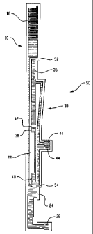
Fig. 4 is an orthogonal view of the exemplary multiple-element antenna 50
shown in Fig.
3 mounted in a mobile communication device 60. The mobile communication device
60
includes a dielectric housing 62 having a top surface 63, a front surface 64,
a first side surface
fib, and a second side surface 68. In addition, the mobile communication
device 60 includes a
transmitter 74 and a receiver 76 mounted within the dielectric housing 62.
The multiple-element antenna structure S0, including the flexible dielectric
substrate 52
on which the antenna 50 is fabricated, is mounted on the inside of the
dielectric housing 62. The
antenna 50 and its flexible substrate 52 are folded from the original, flat
configuration illustrated
in Fig. 3, such that they extend around the inside surface of the dielectric
housing 62 to orient the
antenna structure 50 in multiple perpendicular planes. The top section 14 of
the monopole
portion 10 of the antenna SO is mounted on the first side surface 66 of the
dielectric housing 62
and extends from the first side surface 66 around a front corner 70 to the
front surface 64 of the
dielectric housing 62. The middle section 12 of the monopole 10 extends fully
across the front
surface fi4 of the dielectric housing 62. The bottom section 16 of the
monopole 16 is folded to
extend from the front surface 64 of the housing 62 around another front corner
72 to the second
side surface 68, such that the gain patch 24 is mounted on the front surface
64. The bottom
section 16 is then folded a second time to extend from the second side surface
68 to the top
7
CA 02381043 2002-04-09
surface 63, such that the monopole feeding port 26 is mounted on the top
surface 63 of the
housing 62 relative to the receiver circuitry 76.
The dipole portion 30 of the antenna 50 is folded and mounted across the front
and top
;surfaces 64, 63 of the dielectric housing 62, such that the dipole feeding
ports 44 are mounted on
t:he top surface 63 and the conductor sections 32, 34 are mounted partially on
the front surface 64
and partially on the top surface 63. The dipole feeding ports 44 are
positioned on the top surface
ti3 of the dielectric housing 62 relative to the transmitter circuitry 74.
The monopole feeding port 26 is coupled to the input of the receiver 76, and
the dipole
feeding ports 44 are coupled to the output of the transmitter 74. The
operation of the mobile
communication device 60 along with the transmitter 74 and receiver 76 is
described in more
detail below with reference to Fig. 5.
Fig. 5 is a block diagram of the mobile communication device 60 illustrated in
Fig. 4.
'Che mobile communication device 60 includes a processing device 82, a
communications
subsystem 84, a short-range communications subsystem 86, input/output devices
88-98, memory
devices 100, 102, and various other device subsystems 104. The mobile
communication device
ti0 is preferably a two-way communication device having voice and data
communication
capabilities. In addition, the device 60 preferably has the capability to
communicate with other
<:omputer systems via the Internet.
The processing device 82 controls the overall operation of the mobile
communications
<ievice 60. Operating system software executed by the processing device 82 is
preferably stored
in a persistent store, such as a flash memory 100, but may also be stored in
other types of
memory devices, such as a read only memory (ROM) or similar storage element.
In addition,
system software, specific device applications, or parts thereof, may be
temporarily loaded into a
8
CA 02381043 2002-04-09
volatile store, such as a random access memory (RAM) 102. Communication
signals received
by the mobile device 60 may also be stored to RAM.
The processing device 82, in addition to its operating system functions,
enables execution
of software applications on the device 60. A predetermined set of applications
that control basic
device operations, such as data and voice communications, may be installed on
the device 60
during manufacture. In addition, a personal information manager (PIM)
application may be
installed during manufacture. The PIM is preferably capable of organizing and
managing data
items, such as e-mail, calendar events, voice mails, appointments, and task
items. The PIM
application is also preferably capable of sending and receiving data items via
a wireless network
l 18. Preferably, the PIM data items are seamlessly integrated, synchronized
and updated via the
wireless network 118 with the device user's corresponding data items stored or
associated with a
host computer system. An example system and method for accomplishing these
steps is
disclosed in "System And Method For Pushing Information From A Host System To
A Mobile
Device Having A Shared Electronic Address," U.S. Patent No. 6,219,694, which
is owned by the
assignee of the present application.
Communication functions, including data and voice communications, are
performed
through the communication subsystem 84, and possibly through the short-range
communications
subsystem 86. The communication subsystem 84 includes the receiver 76, the
transmitter 74 and
t:he multiple-element antenna 50, as shown in Fig. 4. In addition, the
communication subsystem
84 also includes a processing module, such as a digital signal processor (DSP)
110, and local
oscillators (LOs) 116. The specific design and implementation of the
communication subsystem
84 is dependent upon the communication network in which the mobile device 60
is intended to
operate. For example, a device destined for a North American market may
include a
9
CA 02381043 2002-04-09
communication subsystem 84 designed to operate within the MobitexTM mobile
communication
>ystem or DataTACTM mobile communication system, whereas a device intended for
use in
l~urope may incorporate a General Packet Radio Service (GPRS) communication
subsystem.
Network access requirements vary depending upon the type of communication
system.
1~or example, in the Mobitex and DataTAC networks, mobile communications
devices are
registered on the network using a unique personal identification number or PIN
associated with
c;ach device. In GPRS networks, however, network access is associated with a
subscriber or user
of a device. A GPRS device therefore requires a subscriber identity module,
commonly referred
to as a SIM card, in order to operate on a GPRS network.
When required network registration or activation procedures have been
completed, the
mobile communication device 60 may send and receive communication signals over
the
communication network 118. Signals received by the monopole portion 10 of the
multiple-
c;lement antenna 50 through the communication network 118 are input to the
receiver 76, which
may perform such common receiver functions as signal amplification, frequency
down
conversion, filtering, channel selection, and analog-to-digital conversion.
Analog-to-digital
conversion of the received signal allows the DSP to perform more complex
communication
functions, such as demodulation and decoding. In a similar manner, signals to
be transmitted are
processed by the DSP 110, and are the input to the transmitter 74 for digital-
to-analog
conversion, frequency up-conversion, filtering, amplification and transmission
over the
communication network via the dipole portion 30 of the multiple-element
antenna 50.
In addition to processing communication signals, the DSP 110 provides for
receiver 76
and transmitter 74 control. For example, gains applied to communication
signals in the receiver
CA 02381043 2002-04-09
'16 and transmitter 74 may be adaptively controlled through automatic gain
control algorithms
implemented in the DSP 110.
In a data communication mode, a received signal, such as a text message or web
page
download, is processed by the communication subsystem 84 and input to the
processing device
82. The received signal is then further processed by the processing device 82
for output to a
display 98, or alternatively to some other auxiliary I/O device 88. A device
user may also
compose data items, such as e-mail messages, using a keyboard 92, such as a
QWERTY-style
keyboard, and/or some other auxiliary I/O device 88, such as a touchpad, a
rocker switch, a
thumb-wheel, or some other type of input device. The composed data items may
then be
transmitted over the communication network 118 via the communication subsystem
84.
In a voice communication mode, overall operation of the device is
substantially similar to
the data communication mode, except that received signals are output to a
speaker 94, and
:signals for transmission are generated by a microphone 96. Alternative voice
or audio 1/O
:subsystems, such as a voice message recording subsystem, may also be
implemented on the
device 60. In addition, the display 98 may also be utilized in voice
communication mode, for
c;xample to display the identity of a calling party, the duration of a voice
call, or other voice call
related information.
The short-range communications subsystem 86 enables communication between the
mobile communications device 60 and other proximate systems or devices, which
need not
necessarily be similar devices. For example, the short-range communications
subsystem 86 may
include an infrared device and associated circuits and components, or a
BluetoothTM
communication module to provide for communication with similarly-enabled
systems and
devices.
11
CA 02381043 2002-04-09
This written description uses examples to disclose the invention, including
the best mode,
and also to enable any person skilled in the art to make and use the
invention. The patentable
scope of the invention is defined by the claims, and may include other
examples that occur to
those skilled in the art.
12