Note: Descriptions are shown in the official language in which they were submitted.
CA 02381113 2002-04-09
TITLE OF THE INVENTION
Substrate Processing Apparatus
BACKGROUND OF THE INVENTION
Field of the Invention
The present invention relates to a substrate processing apparatus
used for processing such as plasma CVD (Chemical Vapor Deposition), low
pressure CVD, metal CVD, insulating film CVD, ion implantation and
etching.
Description of the Background Art
:l0 For semiconductor manufacturing apparatuses for processing
semiconductor substrates such as silicon wafers as one type of the substrate
processing apparatus, various susceptors (ceramics module) for mounting
and heating a wafer have been proposed, some of which have been already
practically used.
:l5 For example, Japanese Patent Laying-Open No. 4-78138 proposes a
semiconductor wafer heating apparatus such as shown in Fig. 8.
Referring to Fig. 8, a semiconductor wafer heating apparatus 101
has a T-shaped cxoss section, and in which a disk-shaped heater portion 102
and a columnar support portion 105 are integrated. Disk-shaped heater
20 portion 102 is formed of ceramic, and a resistance heater 103 is embedded
spirally therein.
Columnar support portion 105 is joined to a center of portion on the
rear surface of a wafer heating surface 102a. An O-ring 109 is provided
between an outer circumferentzal surface of columnar support portion 105
25 and a chamber 104 for air tight sealing. A thermocouple 111 and two
electrodes 103a are embedded in disk-shaped heater portion 102 and
columnar support portion 105, and taken out from chamber 104 through an
upper end surface of columnar support portion 105.
In such heating apparatus 101, when power is supplied to an end
30 portion of resistance heater 103 through electrode 103x, resistance heater
103 generates heat, and wafer heating surface 102a is heated.
According to this publication, heating apparatus 101 can prevent
contamination as experienced by a metal heater, does not suffer from
-1-
CA 02381113 2002-04-09
unsatisfactory thermal efficiency as in an indirect heating method, and does
not suffer from the problem of thermal adhesion onto an infrared
transmission window. Further, in the heating apparatus, corrosion of
electrodes as well as discharge and leakage between electrodes or the
electrode hausing can also be prevented.
However, in heating apparatus 101 having the above described
structure, it is necessary to attach columnar support portion 105 to disk-
shaped heater portion 102 in which resistance heater 103 is embedded.
This results in a complicated structure and hence significantly increases
cost. Further, as columnar support portion 105 supports disk-shaped
heater portion 102, it must have a large cross sectional area and large
thermal capacity. Thus, as the heat generated by resistance heater 103 is
transferred to columnar support portion 105, thermal uniformity of wafer
heating surface 102a of disk-shaped heater portion 102 is made unstable.
Further, in order to attain air tight seal using O-ring 109 at the
contact portion between columnar support portion 105 and chamber 104, it
is necessary to lower the temperature to be 200°C or lower. Thus, the
length of columnar support portion 105 becomes 200 mm or longer, and the
height of the apparatus cannot be made smaller.
Further, in order to support disk-shaped heater 102, in most cases
the columnar support portion 105 is attached to the central portion on the
rear surface of disk-shaped heater portion 102. This poses restrictions on
the position of mounting power supply conductive members or thermocouple
electrically connected to resistance heater 103.
SUMMARY OF THE INVENTION
An object of the present invention is to provide a substrate
processing apparatus that realizes satisfactory thermal uniformity, reduces
cost, is suitable for reduction in size of the apparatus and eases
restrictions
in mounting the power supply conductive members and the like.
The present invention provides a substrate processing apparatus
processing a substrate mounted on a substrate susceptor in a chamber, in
which the susceptor has a flat plate portion having an electric circuitry and
a ceramic base body, and supported by the chamber as at least a surface of
-2-
CA 02381113 2002-04-09
the flat plate portion other than the surface on which the substrate is
mounted is in contact with the chamber.
In the substrate processing apparatus of the present invention, as
the flat plate portion of the ceramic base body is directly in contact with
the
chamber, it becomes unnecessary to provide the columnar support body as in
the prior art on the ceramic base body itself. Namely, the ceramic base
body can be directly placed in the chamber. Thus, the structure of the
ceramic base body itself can significantly be simplified.
The inventors repeated design and experiment to confirm whether
LO such a structure is feasible as a manufacturing apparatus, and found that
substrate processing is possible even under reduced pressure lower than 1
atmospheric pressure, from the following reasons.
In the substrate processing apparatus of the present invention,
when viewed macroscopically, the ceramic base body and the chamber are
simply in point contact, with the contact area being extremely small. Thus,
the quantity of heat transmitted from the ceramic base body to the chamber
by thermal transfer is relatively small. Further, the atmosphere in the
chamber is generally under low pressure, that is, 1 atmospheric pressure or
lower. Thus, the quantity of heat transmitted from the ceramic base body
to the chamber by convection is also small. Further, the chamber is
generally formed of metal, and therefore it has lower emissivity than the
ceramic base body.
Therefore, even when the heat generated by the ceramic base body is
radiated to the chamber, most of the heat is reflected by the chamber and
~5 absorbed again by the ceramic base body. Thus, the quantity of heat
transmitted from the ceramic base body to the chamber is relatively small.
As described above, the quantity of heat transmitted from the
ceramic base body to the chamber through thermal transfer, convection and
radiation is relatively small, and thermal transfer density becomes unifoxm
~30 dependent on the possibility of contact. Therefore, it is not the case
that a
local portion on the ceramic base body transfers heat in a concentrated
manner to the chamber. Thus, influence to the thermal uniformity of the
substrate mounting surface is small. Thus, a substrate processing
-3-
CA 02381113 2002-04-09
apparatus having superior thermal uniformity of the substrate mounting
surface can be provided.
Further, the conventional columnar support portion becomes
unnecessary. Therefore, the cost can significantly be reduced, and the
restrictions in attaching the power supply conductive members and the like
can be eased.
Further, different from the prior art, the columnar support portion
having the length of 200 mm or more does not exist. Therefore, the
chamber itself can be reduced in size. Further, as the chamber can be made
smaller, the substrate processing apparatus itself can be made smaller.
As to the method of fixing the flat plate portion on the chamber, a
recessed portion slightly larger than an outer shape of the flat plate portion
may be formed at a portian of the chamber where the flat plate portion is to
be placed, and the flat plate portion may simply be fitted therein. Thus,
without the necessity of forming a protruded portion on the flat plate
portion,
it is possible to mount the substrate on the substrate mounting surface and
to perform various CVD, etching and other processes under reduced
pressure of lower than 1 atmospheric pressure.
In the present invention, "substrate processing apparatus" includes
a semiconductor manufacturing apparatus and a liquid crystal substrate
manufacturing apparatus, and "substrate" includes a semiconductor wafer
and a transparent substrate (glass substrate) for liquid crystal.
In the above described substrate processing apparatus, preferably,
the electric circuitry includes at least one selected from the group
consisting
of a resistance heater, an electrode for electrostatic chuck and an RF (Radio
Frequency) electrode.
As the resistance heater, the electrode for electrostatic chuck and the
RF electrode are used each by itself or in various combinations as the
electric
circuitry, processing of the substrate in accordance with various different
conditions becomes possible. Haw to combine the resistance heater, the
electrode for electrostatic chuck and the RF electrode may appropriately be
selected dependent on the processing condition.
Here, the electrode for electrostatic chuck and the RF electrode do
-4-
CA 02381113 2002-04-09
not directly generate heat, unlike the resistance heater. However, heat is
build up in the electrostatic chuck at the time of etching, for example, and
in
the RF electrode at the time of plasma generation. Thus, temperature
distribution thereof has an influence on the processing of the wafer or the
liquid crystal substrate. In the substrate processing apparatus of the
present invention, however, the ceramic base body is :in direct contact with
the chamber as described above. Therefore, :temperature distribution
generated at the electrode for electrostatic chuck and the RF electrode is
very uniform as compared with th.e conventional structure.
Preferably, in the substrate processing apparatus described above,
there is a small space between the flat plate portion and the chamber which
are in contact with each other.
As a small space exist between the flat plate portion and the
chamber that are in contact with each other, the flat plat portion and the
:15 chamber are in point contact when viewed macroscopically, and the contact
area is very small. Thus, the quantity of heat transmitted from the flat
plate portion to the chamber by thermal transfer is relatively small, as
already described.
Preferably, the substrate processing apparatus further includes a
:?0 power supply conductive member electrically connected to the electric
circuitry and drawn out from the chamber, and a temperature measurement
terminal inserted from the outside to the inside of the chamber for
measuring temperature of the ceramic base body. The portion at which the
power supply conductive member and the temperature measuring terminal
~5 pass through the chamber is air-tightly sealed on the chamber side.
In the structure of the present invention, the electric circuitry such
as the resistance heater, the electrode for electrostatic chuck and the ftF
electrode is formed on the ceramic base body, and therefore, it is necessary
to
draw out a power supply conductive member to the outside of the chamber.
c30 Further, even when a thermocouple is used as a temperature measurement
sensor for measuring the temperature of the ceramic base body itself, it is
necessary to draw out the lead portion of the thermocouple to the outside of
the chamber, as in the case of the power supply conductive member. In
-5-
CA 02381113 2002-04-09
order to process the wafer or the liquid crystal substrate in a reduced
pressure of lower than 1 atmospheric pressure in the chamber, air-tightness
of the chamber must be ensured. As a method of ensuring air-tightness, it
is necessary to realize air-tight sealing between the power supply terminal
or the thermocouple drawn out from the ceramic base body and the chamber.
An O-ring formed of resin or rubber, may be used as means for ensuring
air-tight sealing.
In the present invention, "air-tight sealing on the chamber side"
refers to air-tight sealing established between the chamber and a member
other than the ceramic base body.
Preferably, in the substrate processing apparatus, the power supply
conductive member is covered by a first coating member of the same
material as the ceramic base body, at least in the chamber.
As the power supply conductive member is covered by the same
1.5 coating member as the ceramic base body, corrosion of each power supply
conductive member caused by the influence of gas or plasma used in the
chamber can be prevented.. The coating member may be joined to the
ceramic base body to maintain air-tightness with respect to the chamber,
and it may establish air-tightness with the outside when the coating
member is extended to the air-tight sealing portion between the chamber
and outside, for example, to the 0-ring attached to the chamber.
There is no limitation as to the method of joining the ceramic base
body and the coating member. Known methods may be used as the method
of joining. For example, it may be joined by using a metal blazing material
containing an active metal such as titanium. Alternatively, a metal film
may be formed by a thin film method such as vapor deposition or
metallization layer may be formed by a thick film method such as screen
printing, on the ceramic base body or on the coating member, plating may be
performed as needed, and the joining may be established by blazing
material. Alternatively, glass or ceramic may be used as a joining layer.
Such joining layer may appropriately be selected dependent on the condition
of use.
Preferably, in the above described substrate processing apparatus,
-6-
CA 02381113 2002-04-09
the temperature measurement terminal is covered by a second coating
member which is the same as the material of the cexamic base body, at least
in the chamber.
When the temperature measurement sensor is a thermocouple, for
example, the thermocouple is arranged close to the ceramic base body to
measure the temperature of the ceramic base body. Here, when the
thermocouple is covered with a coating member of the same material as the
ceramic base body, corrosion of the terminal caused by the influence of gas or
plasma used in the chamber can be prevented.
Further, when the coating member is extended to the airtight
sealing portion between the chamber and the outside, for example to the O-
ring attached to the chamber, air-tightness with the outside can be ensured.
Further, it is possible to join the ceramic base body and the coating member.
There is no restriction as to the method of joining and a known method may
be used. For example, it may be joined by using a metal blazing material
containing an active metal such as titanium. Alternatively, a metal film
may be formed by a thin film method such as vapor deposition or
metallization layer may be formed by a thick film method such as screen
printing, on the ceramic base body ox on the coating member, plating may be
performed as needed, and the joining may be established by blazing
material. Alternatively, glass ox ceramic may be used as a joining layer.
Such joining layer may appropriately be selected dependent on the condition
of use.
When the power supply conductive member and the temperature
measurement sensor are covered by the coating members of the same
material as the ceramic, it is possible to provide a plurality of power supply
conductive members and a plurality of temperature measurement sensors in
the coating member. This enables reduction in number of the coating
member.
Further, the coating member serves to protect the power supply
conductive member and the temperature measurement sensor from the
chamber atmosphere as described above, and it does not serve to support the
ceramic base body onto the chamber. Thus, the size of the coating member
-7-
CA 02381113 2002-04-09
can significantly be made smaller than the size of the conventional columnar
support portion. Thus, the joint ~ contact area between the coating
member and a ceramic base body can also be made smaller, and thermal
capacity of the coating member itself can be made smaller. Thus, quantity
of heat transmitted to the coating member becomes smaller, and hence
thermal uniformity of the substrate mounting surface of the ceramic base
body is not so much degraded as in the prior art.
Further, as the coating member does not support the ceramic base
body on the chamber, the cross sectional area of the member can be made
small. Thus, there is no restriction as to the mounting position.
Conventionally, one central portion of the disk-shaped heater portion must
have a holding function and the columnar support portion must. be attached
thereon. By contrast, in the present invention, it is possible to attach the
coating members at a plurality of positions other than the substrate
mounting surface of the ceramic base body. Thus, electrode position can be
selected freely in designing the electric circuitry. Further, the temperature
measurement sensor can also be freely attached to the surface other than
the substrate mounting surface of the ceramic base body. Therefore,
temperatures of any number of portions may be measured as needed. Thus,
;~0 the temperature of the ceramic base body can be monitored and controlled
with higher accuracy.
Preferably, the above described substrate processing apparatus
further includes a power supply conductive member electrically connected to
the electric circuitry and drawn out from the chamber, and a temperature
w5 measurement terminal inserted from the outside to the inside of the
chamber for measuring temperature of the ceramic base body. The portion
at which the power supply conductive member and the temperature
measurement terminal pass through the chamber is air-tightly sealed as the
flat plate portion and chamber are joined.
ci0 As the flat plate portion is partially joined to the chamber, air-
tightness of the temperature measurement sensor and the power supply
terminal can be maintained. There is no specific restriction as to the
method of joining the chamber and the flat plate portion. For example, a
_g_
CA 02381113 2002-04-09
blazing material containing active metal such as silver, copper, gold,
platinum, palladium, nickel, aluminum, titanium, or niobium may be used.
As to the method of using the blazing material, direct joining by a metal
blazing member containing an active metal such as titanium is possible, for
example. Further, a metal may be vapor-deposited by the thin film method
at that portion of the ceramic which is to be sealed, and the blazing material
may be caused to flow thereto, to attain joint. Further, the chamber and
the flat plate portion may be joined by glass. Dependent on the processing
of the semiconductor or the liquid crystal substrate, some of the materials
including the above described blazing materials, vapor-deposited films and
glass may not be used. Therefore, it is necessary to select an appropriate
material in accordance with the use.
Preferably, in the above described substrate processing apparatus,
at least a part of a surface of the chamber that is in contact with the flat
plate portion is a mirror finished surface.
As described above, the heat generated by the ceramic base body is
transmitted to the chamber through radiation, heat transfer and convection.
Here, when the chamber side has a mirror-finished surface, the heat
radiated from the ceramic base body would be reflected by the chamber at a
higher ratio, so that the quantity of heat transmitted to the chamber is
significantly reduced, which is very much effective in suppressing
temperature increase.
Preferably, in the above described substrate processing apparatus,
at least a surface other than the substrate mounting surface of the substrate
susceptor is a mirror-fmished surface.
When the heat generated in the ceramic base body is radiated to the
outside of the ceramic base body and the surface of the substrate susceptor is
mirror-finished, the heat would be reflected at the surface with higher ratio,
and the ratio of thermal radiation to the outside of the substrate susceptor
decreases. Thus, temperature increase of the chamber can be suppressed.
The surface for mounting the wafer and the liquid crystal substrate,
however, need not be mir:ror-finished, as it is necessary to heat the wafer
and the liquid crystal substrate.
_9_
CA 02381113 2002-04-09
Preferably, in the substrate processing apparatus, surface roughness
of at least one of the chamber surface which is in contact with at least the
flat plate portion and the at least one surface other than the substrate
mounting surface of the substrate susceptor, is Ra <_ 0.2 ~.m.
When at least the chamber surface at least in contact with the flat
plate portion or at least a part of the surface other than the substrate
mounting surface of the substrate susceptor is mirror-finished, temperature
increase of the chamber can effectively be suppressed. More specifically,
when the surface roughness is Ra <_ 0.2 Vim, temperature increase can more
effectively be suppressed. Thus, temperature increase of the chamber can
be suppressed, and the quantity of heat generation by the resistance heater
formed in the ceramic base body, that is, the output, can be lowered.
Preferably, the substrate processing apparatus further includes a
cooling apparatus provided near a portion of the chamber which is in contact
with the flat plate portion.
Though the quantity of heat transmitted from the ceramic base body
to the chamber is small, the heat is transmitted to some extent to the
chamber, through radiation, heat transfer, convection and through the
power supply conductive member, the lead of the temperature measurement
sensor and the coating member. Failure of air-tightness resulting from
thermal degradation of the O-ring formed of rubber or resin maintaining
airtight seal with the outside, can be prevented by the cooling apparatus.
Various methods may be selected for the cooling apparatus,
dependent on the degree of temperature increase of the chamber. When
the temperature increase is small, a fin may be attached, for example, and
when temperature still increases, a fan may be additionally provided to the
fin. Further, a liquid-cooling apparatus using a coolant such as water may
be attached. Further, such methods may be combined to efficiently cool the
chamber.
Further, in order to thermally protect the O-ring formed of resin or
rubber ensuring air-tightness between the chamber and the outside, the
space between the coating member and the chamber to which the cooling
apparatus is attached may be filled with a thermally conductive member.
-10-
CA 02381113 2002-04-09
More specifically, a soft metal, for example, indium, may be filled between
the coating member and the chamber, on the outer side of the chamber
where the O-ring is attached, so that the heat that has been transmitted to
the coating member is leaked to the chamber side, and the temperature near
the O-ring can be lowered. Thus, the life of the O-ring can be improved,
and reliability of air-tightness can be improved. More specifically, even
when the resistance heater placed in the ceramic base body operates
abnormally, resulting in abnormal heat, thermal destruction of the O-ring
and the leakage of atmospheric air into the chamber can be prevented.
Preferably, the substrate processing apparatus further includes a
push pin inserted from the outside to the inside of the chamber, for pushing
up the substrate mounted on the substrate susceptor from the substrate
susceptor. The portion at which the push pin passes through the chamber
is air-tightly sealed, between the push pin and the chamber.
Thus, it is possible to use a push pin when the wafer or the liquid
crystal substrate is to be removed from the substrate mounting surface of
the substrate susceptor. When the push pin is to be taken out from the
chamber, it is necessary to air-tightly seal the push pin as well, as the
chamber is used under low pressure. Though there is no specific restriction
as to the method of sealing here, an O-ring formed of resin or rubber may be
used.
Preferably, the substrate processing apparatus described above is
used under a low pressure of 133 x lOPa or lower.
Under the low pressure of 133 x lOPa or lower, quantity of heat
transmitted by convection from the ceramic to the chamber becomes smaller.
Therefore, use under such a low pressure is particularly preferable.
Preferably, the substrate processing apparatus described above is
used for any of the processes including chemical vapor deposition using
plasma, chemical vapor deposition under low pressure, chemical vapor
deposition for forming a metal layer, chemical vapor deposition for forming
an insulating film, ion implantation and etching.
As various portions are air-tightly sealed as described above, use
under low pressure of 1 atmospheric pressure or lower is possible without
-11-
CA 02381113 2002-04-09
any problem. Therefore, the apparatus can preferably be used for chemical
vapor deposition using plasma, chemical vapor deposition under low
pressure, chemical vapor deposition for forming a metal layer, chemical
vapor deposition for forming an insulating film, ion implantation, plasma
etching and optical etching.
Preferably, in the substrate processing apparatus, the ceramic base
body includes at least one selected from the group consisting of aluminum
oxide, aluminum nitride, silicon nitride and silicon carbide.
These ceramic materials generally have heat resistance and
YO relatively high corrosion resistance as they are dense. Thus, a substrate
processing apparatus which realizes both satisfactory heat resistance and
corrosion resistance can be provided.
Preferably, in the substrate proces~ng apparatus described above,
the ceramic base body is of aluminum nitride.
:l5 Among the ceramic materials mentioned above, aluminum oxide
(alumina) is particularly suitable for plasma etching. As to silicon carbide,
a sintered body of silicon carbide of high impurity that is sintered without
adding any sintering assistant agent is used.
Among the ceramics mentioned above, alumina has low thermal
20 conductivity, and therefore low thermal shock resistance. Therefore, it is
impossible to abruptly increase or decrease temperature during the steps of
manufacturing the semiconductor. As to silicon carbide, silicon carbide
itself is conductive, and therefore an electric circuit cannot directly be
formed thereon. By contrast, aluminum nitride has superior corrosion
25 resistance and relatively high thermal conductivity, and thus superior
thermal shock resistance. Thus, abrupt increase and decrease of
temperature during the steps of manufacturing the semiconductor substrate
becomes possible. Further, when there is provided a resistance heater,
variation in temperature of the substrate mounting surface becomes
30 relatively small, enabling stable processing of the substrate.
Preferably, in the substrate processing apparatus, the ceramic base
body includes a sintering assistant agent including a rare earth.
When aluminum nitride is used as the material of the ceramic base
-12-
CA 02381113 2002-04-09
body, abrupt increase and decrease of temperature becomes possible and
stable substrate processing becomes possible, as described above.
Aluminum nitride, however, is generally a sintering retardant substance,
and therefore, a sintered body thereof is fabricated by adding an appropriate
amount of sintering assisting agent. The sintering assistant agent used at
this time is generally a rare-earth element compound, or an alkali earth
metal element compound. When aluminum nitride sintered body prepared
by.adding alkali earth metal compound is used, alkali earth metal
compound existing between aluminum nitride particles of the sintered body
is etched during processing of the substrate with plasma or corrosive gas, so
that aluminum nitride particles slip off from the sintered body., It is
confirmed that when the slipped aluminum nitride particle contaminate the
chamber, substrate property of the wafer or the liquid crystal substrate are
significantly damaged. Thus, from experience, it is considered preferable
to use rare-earth element compound, which is relatively strong against
etching, as the sintering assistant agent.
Preferably, in the substrate processing apparatus described above,
the rare-earth included in the sintering assistant agent is yttrium, and the
content of the sintering assistant agent is at least 0.05 mass % and at most
;t0 1.0 mass %.
Among the rare earths mentioned above, yttrium has particularly
high corrosion resistance. When the content of the sintering assistant
agent including yttrium is smaller than 0.05 mass %, the amount of the
sintering assistant agent is too small, so that small pores result in the
~5 sintering body, from which etching proceeds. When the content of the
sintering assistant agent including yttrium exceeds 1.0%, "aggregation" of
the sintering assistant agent is generated at the grain boundary of
aluminum nitride particles, from which etching tends to proceed.
There is no specific restriction as to the method of manufacturing the
30 ceramic fabricated in accordance with the present invention. For example,
the sintering assistant agent may be added as needed to raw material
powder of ceramic, a binder, and an organic solvent may be added and mixed
by a ball mill, for example. The resulting slurry may be formed to a sheet
-13-
CA 02381113 2002-04-09
by a doctor blade method, and by stacking the sheets, a compact may be
formed. Further, it is possible to stack the sheets with an electric circuit
formed on any of the sheets by screen printing, for example, of a metal
having high melting point such as tungsten, molybdenum, or tantalum.
The resulting compact is sintered at a prescribed temperature in a non-
oxidizing atmosphere, to provide a ceramic sintered body. The ceramic
body may be appropriately processed, that is, it may be cut, polished, or
ground, as needed.
The foregoing and other objects, features, aspects and advantages of
:l0 the present invention will become more apparent from the following
detailed
description of the present :invention when taken in conjunction with the
accompanying drawings.
BRIEF DESCRIPTION OF THE DRAWINGS
Fig. 1 is a cross section schematically showing a structure of a
:l5 substrate processing apparatus in accordance with one embodiment of the
present invention, which corresponds to the cross section taken along the
line I-I of Fig. 2.
Fig. 2 is a plan view showing a manner of arrangement of through
holes in a contact surface between a ceramic module and a chamber.
~!0 Fig. 3 is a schematic cross section illustrating a thermocouple
directly in contact with the ceramic base body.
Fig. 4 is a schematic cross section showing a structure when an
electrode for electrostatic chuck or an RF electrode is used as the electric
circuitry.
~5 Fig. 5 is a schematic cross section showing a structure when a
resistance heater, an electrode for electrostatic chuck and an RF electrode
are used combined for the electric circuitry.
Fig. 6 is a plan view showing a pattern of the resistance heater.
Fig. 7 is a plan view showing a pattern of the electrode for
0 electrostatic chuck or the RF electrode.
Fig. 8 is a cross section schematically showing a structure of a
semiconductor wafer heating apparatus disclosed in Japanese Patent
Laying-Open No. 4-78138.
- 14-
CA 02381113 2002-04-09
DESCRIPTION OF THE PREFERRED EMBODIMENTS
Embodiments of the present invention will be described in the
following with reference to the figures.
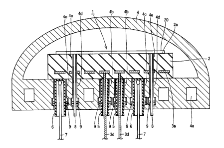
Referring to Fig. 1, the substrate processing apparatus in accordance
with the present embodiment is for processing a substrate such as a
semiconductor wafer or a transparent substrate for liquid crystal. The
apparatus mainly includes a ceramic module 1 for mounting and heating the
substrate, and a chamber 4 containing the ceramic module 1 therein.
The ceramic module 1 has a flat, plate shape mainly formed of a
ceramic base body 2, and an electric circuitry, for example, a resistance
heater 3a, is embedded in ceramic base body 2. On a substrate mounting
surface 2a of ceramic module 1, a substrate 20 such as a semiconductor
wafer or a transparent substrate for liquid crystal is mounted. A surface of
ceramic base body 2 opposite to the surface for mounting substrate 20 is in
direct contact with chamber 4 and thus supported by chamber 4.
Though the surface of ceramic base body 2 is shown fully in contact
with the chamber 4 in the figure, actually, there are a number of small
spaces between ceramic substrate 2 and chamber 4, and therefore, when
viewed macroscopically, ceramic base body 2 and chamber 4 are in point
contact.
Referring to Fig. 2, in the contact surface between ceramic module 1
and chamber 4, there are a plurality of through holes 4b, 4c and 4d, passing
through chamber 4.
Referring to Fig. 1, through hole 4b is provided for inserting from the
outside of chamber 4, a power supply conductive member 3d that is
electrically connected to resistance heater 3a. Through hole 4c is provided
for inserting, from the outside of chamber 4, a temperature measurement
sensor, for example, a thermocouple 7, for measuring temperature of ceramic
base body 2, to be close to ceramic base body 2. Through hole 4d is provided
for inserting, from the outside of the chamber, a push pin 8 for pushing up
the substrate 20 mounted on ceramic module 1. Ceramic module 1 is
provided with a through hole 4e though which push pin 8 is passed.
Power supply conductive member 3d electrically connected to
-15-
CA 02381113 2002-04-09
resistance heater 3a has its periphery covered by a coating member 5 at
least in chamber 4. Thus, corrosion of resistance heater 3a by gas or
plasma in chamber 4 is prevented. Coating member 5 is of the same
material as ceramic base body 2. An O-ring 9 is provided between outer
circumferential surface of coating member 5 and inner circumferential
surface of through hole 4b, to attain airtight sealing.
Thermocouple '7 as the temperature measurement sensor also has its
periphery covered by coating member 6 at least in chamber 4, so that
corrosion by gas or plasma in chamber 4 is prevented. Coating member 6 is
of the same material as ceramic base body 2. An O-ring 9, for example, is
provided between outer circumferential surface of coating member 6 and
inner circumferential surface of through hole 4c, to attain airtight sealing.
Each of the through holes 4b and 4c is air-tightly sealed, as ceramic
base body 2 is in contact with chamber 4.
An O-ring 9 is provided between the outer circumference of push pin
8 and inner circumference of throughhole 4d, to attain airtight sealing.
In the vicinity of a portion where ceramic module 1 is arranged of
chamber 4, a liquid cooling apparatus 4a using a coolant such as water is
provided. The cooling apparatus 4a is not limited to a liquid cooling
apparatus, and it may be a cooling apparatus provided with a fin or fan, for
example.
It is preferred that at least that surface of chamber 4 which is in
contact with ceramic base body 2 is mirror-finished. Further, it is preferred
that surfaces of ceramic module 1 other than the substrate mounting surface
2a are mirror-finished. Further, the surface of ceramic module 1 which is
in contact with chamber 4 is mirror-finished.
Preferably, the surface roughness of the mirror finished portions is
Ra <_ 0.2 Etm.
Preferably, the substrate processing apparatus in accordance with
the present embodiment is used under a low pressure of 133 x lOPa or lower.
Further, the apparatus is preferably used for CVD using plasma, CVD
under low pressure, CVD for forming a metal layer, CVD for forming an
insulating film, ion implantation or etching. Preferably, the material of
16-
CA 02381113 2002-04-09
ceramic base body 2 is aluminum oxide (alumina), aluminum nitride, silicon
nitride, silicon carbide, or an arbitrary combination of these. More
preferably, the material is aluminum nitride. When the material of
ceramic base body 2 is aluminum nitride, it is preferred that ceramic base
body 2 includes sintering assistant agent including a rare earth.
Preferably, the rare-earth included in the sintering assistant agent is
yttrium. The content of the sintering assistant agent is preferably at least
0.05 mass % and at most 1.0 mass %.
Though a structure in which coating member 6 is positioned between
thermocouple 7 and ceramic base body 2 has been described with reference
to Fig. 1, thermocouple 7 may be arranged in direct contact with the surface
of ceramic base body 2, as shown in Fig. 3.
Though an example in which resistance heater 3a only is used as the
electric circuit has been described with reference to Fig. 1, only an
electrode
3b for electrostatic chuck or only an RF electrode 3c may be used as the
electric circuitry as shown in Fig. 4. Alternatively, resistance heater 3a,
electrode 3b for electrostatic chuck and RF electrode 3c may be arbitrarily
combined as shown in Fig. 5. The combination may include the
combination of resistance heater 3a and electrode 3b of electrostatic chuck,
the combination of resistance heater 3a and RF electrode 3c, the
combination of electrode 3b for electrostatic chuck and RF electrode 3c, and
the combination of resistance heater 3a, electrode 3b for electrostatic chuck
and RF electrode 3c.
Preferably, planar pattern of resistance heater 3a has a heating
portion 3az having circular patterns and terminal portions 3a~positioned at
opposing ends of heating ;portion 3az, as shown in Fig. 6. Heating portion
3aa is patterned such that it does not interfere with the push pin 8.
Electrode 3b for electrostatic chuck or RF electrode may be formed to
such a pattern as shown in Fig. 7. The electrode 3b for electrostatic chuck
or RF electrode 3c is also patterned not to interfere with push pin 8.
Though a structure in which both surfaces of resistance heater 3a
are sandwiched by ceramic base body 2 has been described in the
embodiment above, the surface opposite to the substrate mounting surface
- 17-
CA 02381113 2002-04-09
2a of resistance heater 3a may be covered by a protective layer formed of a
material other than ceramics.
Examples of the present invention will be described in the following.
(Example 1)
Slurry samples were prepared by adding an organic solvent and a
binder to ceramic powders of respective compositions as listed in Table 1
below, and mixing in a ball mill. The resulting slurry samples were formed
to sheets, by doctor blade method. On the resulting sheets, by resistance
heater circuit, an electrode for electrostatic chuck and an RF electrode (for
1.0 generating plasma) are formed as needed, by screen printing, using
tungsten paste. Thereafter, the resulting sheets are stacked, degreased
and sintered in a non-oxidizing atmosphere, portions through which push
pins are to be inserted are drilled, and ceramic base bodies were thus
fabricated.
1.5
Table 1
Sam 1e Main Component Additive
1 Aluminium nitride None
2 Aluminium nitride YsOa 0.05 mass~
3 Aluminium nitride YaOs 0.5 mass%
4 Aluminium nitride YaOs 1.0 mass%
5 Aluminium nitride YaOs 3.0 mass's
6 Aluminium nitride EuaOs 0.5 mass%
? Aluminium nitride YbzOs 0.5 mass%
8 Silicon carbide None
9 Alumina M 0 0.5 mass%
Alumina None
11 Silicon nitride YZOs 0.6 mass%
Thereafter, at portions of these ceramic base bodies where the power
supply conductive member and the temperature measurement sensor
(thermocouple) are to be attached, coating members of the same material as
the ceramic base bodies are attached. As to the method of attachment,
glass mainly containing alumina is used as an adhesive layer. Here, each
coating member'used has an inner diameter of 2.0 mm and outer diameter of
-18-
CA 02381113 2002-04-09
3.0 mm. Thereafter, the power supply conductive members and
thermocouples are attached, and the resulting bodies are mounted in a
chamber. Here, the chamber has a recessed portion of which inner
diameter is slightly larger than each ceramic base body, at the placing
portion, and therefore, the ceramic base body can be placed stationary.
Thereafter, the ceramic base body is attached to the chamber contact surface,
the power supply conductive member and the thermocouple are placed in a
coating member, the push pin is placed at a prescribed position, and these
are air-tightly sealed on the chamber side, by O-rings, respectively.
YO Thereafter, a silicon wafer or a glass substrate for liquid crystal is
mounted on the substrate mounting surface of each ceramic body. The
chamber is evacuated, power is supplied through the power supply
conductive member to the resistance heater, the electrode for electrostatic
chuck and/or RF electrode formed on the ceramic base body, and reaction gas
1.5 is introduced to the chamber as needed. Each process is performed at
550°C. As a result, prescribed processings can be done on the silicon
wafer
and the substrate for liquid crystal. Namely, it is found that the resistance
heater, the electrode for electrostatic chuck and the RF electrode all operate
satisfactory in the present structure, which is a simplified structure.
20 Thermal uniformity of the ceramic base bodies at 550°C is as shown
in Table
2 below.
Table 2
Thermal
Sample oo p~ nt Additive Conductive U~ormity
at
650C
1 A1N None 85 *5.8
2 AlN YaOs 0.05 mass 156 t2.7
%
3 A1N YzOs 0.6 mass % 192 X2.3
4 A1N _ L90 t2.3
YaOs 1.0 mass %
5 A1N YaOs 3.0 mass % 187 f2.3
6 A1N EuzOa 0.5 mass 188 t2.3
%
7 A1N YbzOs 0.6 mass 185 X2.4
%
8 SiC None :173 t2.5
9 AlzOa M 0.5 mass % 23 t9.2
AlzOa None 21 f9.0
11 SiaOa YaOs 0.5 mass % 35 X7.3
-19-
CA 02381113 2002-04-09
(Example 2)
Thereafter, ceramic base bodies used in Example 1 were heated to
750°C in vacuum. Temperature near the 0-rings were measured, and it
was 132°C in Sample 3. The 0-ring used here has the heat resistance up
to
150°C, and therefore there was no leakage in the chamber. Here, the
thermal uniformity of the substrate mounting surface was f3.6°C.
Further, a cooling water is caused to flow to the chamber, so as to
cool the chamber. As a result, the temperature near the O-rings was
decreased to 38°C. Thermal uniformity of the substxate mounting surface
was t3.?°C.
Then, indium as a soft metal was filled, on the outer side of O-ring
with respect to the chamber, between the chamber and the coating member.
As a result, the temperature near the O-ring was decreased to
22°C.
Thermal uniformity of the substrate mounting surface was X3.7°C.
(Example 3)
Samples corresponding to Sample 3 used in Example 2, which have
surface roughness of Ra = 0.7, 0.2 and 0.07 E,un, respectively, on the side
opposite to the substrate mounting surface were prepared. Further,
chambers having ceramic base body placing surfaces with a surface
roughness of Ra = 0.8, 0.2 and 0.05 Nxn, respectively, were prepared.
Thereafter, respective ceramic base bodies were placed in the chambers,
heated to 750°C, and the temperature of the O-ring was measured. The
result is as shown in Table 3.
Table 3
O-rin Tem erature
Surface Roughness
of Ceramic
Base Body
(R,a: Eam)
0.7 0.2 0.07
Surface 0,8 132C 80C 72C
h
R
oug
ness 0.2 38C 32C 31C
of
Chamber
(R,a:~m) 0.05 35C 30C 28C
Thermal uniformity of the substrate mounting surface was, in each
-20-
CA 02381113 2002-04-09
case, f3.7°C. Output of the ceramic base bodies (power lead to ceramic
base
body) was also measured, which was as shown in Table 4.
Table 4
Surface Roughness
of Ceramic
Base Body
(Ra: wm)
0.7 0.2 0.0?
Surface O,g 1230W 928W 855W
hness
Rou
g 0.2 652W 619W 608W
of
Chamber
0.05 631W 605W 594W
(Example 4)
Ceramic base bodies similar to those of Example 1 were prepared.
The resistance heater formed on each of the ceramic base bodies was divided
into a central zone 1 and an outer zone 3, which were adopted to be
separately controllable. The thermocouple and the power supply
conductive member covered with coating members of the same material as
the ceramic base body similar to those used in Example 1 were provided, at
three portions at the outex portion and one at the central portion of the
ceramic base body, amount of power supply to the resistance heater in each
zone was adjusted while monitoring the temperature, and the ceramic base
body was heated to 550°C. Thermal uniformity at that time was as shown
in Table 5.
-21-
CA 02381113 2002-04-09
Table 5
Thermal
Sampleco ponent Adclitive ConductivityU'~ormity
at
550C
1 AlN None 85 f4.2
2 A1N YaOs 0.05 mass 156 f2.1
/.
3 A1N YaOs 0.5 mass % 192 X1.8
4 AlN YaOs 1.0 mass % 190 X1.8
A1N YaOs 3.0 mass ~ 18? X1.8
6 A1N EuzOs 0.5 mass 188 t1.9
/.
7 A1N YbaOs 0. 5 mass 185 t1.9
%
8 SiC None 1?3 X2.0
9 AlaOs M 0.5 mass ~ 23 f?.3
AlzOs None 21 f7.5
11 Sia04 YaOs 0.5 mass %) 3 5 f6.1
From the foregoing, it could be understood that by increasing the
number of portions fox temperature measurement and by adjusting amount
5 of power supply to each zone, thermal uniformity could be improved.
(Example 5)
Substrate surface of each of the ceramic sintered bodies used in
Example 1 was polished. Practical usability of each sample thus processed
was confirmed in the following manner. A disk-shaped heater was
10 prepared by embedding tungsten (V~ filament in a matrix of separately
prepared aluminum nitride ceramic. Thereafter, each sample was
mounted on the heater, and placed in a vacuum chamber of a plasma
generating apparatus that employs high frequency of 13.56 MHz. Each of
the samples was processed for 5 hours in an environment of CFa gas with
1.5 plasma density of 1.4 W/cm2 at a heating temperature of 100°C.
Thereafter,
density of etching craters of the plasma irradiated surface was inspected.
The density of the etching crater was inspected by using a scanning electro
microscope, and a number of craters of which maximum opening diameter is
at least 1 ~,m existing in an arbitrary view field of 1000 ~m2 of the surface
was counted. The result is as shown in Table 6.
-22-
CA 02381113 2002-04-09
Table 6
Sample com onent Additive NDefects f
1 A1N None 17
2 A1N YaOa 0.05 mass % 10
3 AlN YaOa 0.5 mass % 5
4 A1N YaOs 1.0 mass % 5
A1N YaOa 3.0 mass % 14
6 AlN EuaOs 0.5 mass % 13
7 AlN YbaOs 0.5 mass % 12
8 SiC None 19
9 AlaOs M 0 0.5 mass % 23
AlaOs None 21
~- _ 1l_ r S13O4~ YaOa (0.5 mass %) 36
From the results, it could be understood that when the content of the
sintering assistant agent including yttrium was at least 0.05 mass % and at
5 most 1.0 mass %, the number of etching crater was made small.
(Example 6)
Using Sample 3 of Example 1, the ceramic was heated to 750°C in
the atmosphere of 133Pa, 133 x lOPa, 133 x 50Pa and 133 x 760Pa in the
same apparatus by the same method as in Example 1, and the temperature
10 of the chamber near the 0-ring was measured. As a result, the
temperature was 132°C at;133Pa, 133°C at 133 x lOPa,
148°C at 133 x 50Pa
and 589°C at 133 x 760 Pa. Thus, it could be understood that the amount
of
heat transmission to the chamber caused by convection increased as the
inner pressure was increased.
(Comparative Example 1)
For each of the samples used in Example 1, a cylindrical support
portion having an outer diameter of 80 mm, inner diameter of 70 mm and
the length of 250 mm formed of the same material as the ceramic was joined
by the same method as in Example l, at the central portion on the surface
opposite to the substrate mounting surface. Thereafter, the power supply
conductive member and the thermocouple were attached. Then, an end
portion on that side which. is not joined to the cylindrical support portion
was air-tightly sealed with the chamber using an O-ring, and the samples
-23-
CA 02381113 2002-04-09
were heated to 550°C to measure thermal uniformity. The result is as
shown in Table 7.
Table 7
Main Thermal Thermal
Samplecomponent Additive ConductivityUniformity
at
550 C
1 A1N None 85 f7.3
2 A1N YsOa 0.05 mass 156 t5.2
~
3 AlN Y~Os 0.5 mass ~G 192 X4.6
4 AlN YaOa 1.0 mass ~) 190 f4.6
A1N YaOa 3.0 mass /. 187 t4.7
6 A1N EusOa 0.5 maSS 188 f4.?
~
7 A1N YbaOa 0.5 mass 185 f4.7
/a
8 SiC None 173 X4.9
9 AlaOa M 0 0.5 mass % 23 111.5
1O A12O3 None 21 f 10.8
11 SisO.~ Y~Os (0.5 mass 35 t9.3
rb
5.
From the result shown in Table 7, it could be understood that
thermal uniformity was degraded when the cylindrical support portion was
provided.
(Example 7)
lo~ The ceramic base bodies used in Example 1 and the ceramic base
bodies used in Comparative Example 1 were positioned in a chamber. Here,
the height of the chamber was 120 mm for Example 1, and the height was
380 mm for comparative Example 1. Thus, it was understood that by the
method of the present invention, characteristics could be improved as
represented by the examples described above while the size of the chamber
was significantly reduced. Further, as the chamber could be made smaller,
the manufacturing apparatus itself could be made smaller.
(Example 8)
Ceramic base bodies similar to those of Example 1 were fabricated.
20~ Thereafter, portions of the chamber at which the temperature measurement
terminal and the power supply conductive member of the ceramic base body
are to be attached were drilled. Outer circumferential portions of the holes
thus formed and the ceramic base body were adhered by an aluminum
-24-
CA 02381113 2002-04-09
blazing member. Thereafter, similar processing as in Example 1 was
performed, and it was confirmed that prescribed processings could be
performed on the silicon wafer and the substrate for liquid crystal at
550°C
in the similar manner as in Example 1. More specifically, it was found that
the resistance heater, the electrode for electrostatic chuck and the RF
electrode all operated normally in the present structure.
As described above, according to the present invention, the flat plate
portion of the substrate susceptor is in contact with the chamber and thus
directly supported by the chamber. Thus, a substrate processing apparatus
can be obtained in which thermal uniformity can be improved, which cost
can be reduced, suitable for reducing the size and in which restrictions in
mounting power supply conductive members and the like can be eased.
Although the present invention has been described and illustrated in
detail, it is clearly understood that the same is by way of illustration and
example only and is not to be taken by way of limitation, the spirit and scope
of the present invention being limited only by the terms of the appended
claims.
-25-