Note: Descriptions are shown in the official language in which they were submitted.
CA 02381265 2002-O1-29
WO 01/97250 PCT/USO1/16622
TITLE: OPTICAL MAGNETRON FOR HIGH EFFICIENCY PRODUCTION
OF OPTICAL RADIATION, AND 1/2~ INDUCED PI-MODE
OPERATION
Technical Field
The present invention relates generally to light sources, and more
particularly to a high efficiency light source in the form of an optical
magnetron.
Background of the Invention
Magnetrons are well known in the art. Magnetrons have long served as
highly efficient sources of microwave energy. For example, magnetrons are
commonly employed in microwave ovens to generate sufficient microwave energy
for heating and cooking various foods. The use of magnetrons is desirable in
that
they operate with high efficiency, thus avoiding high costs associated with
excess
power consumption, heat dissipation, etc.
Microwave magnetrons employ a constant magnetic field to produce a
rotating electron space charge. The space charge interacts with a plurality of
microwave resonant cavities to generate microwave radiation. Heretofore,
magnetrons have been generally limited to maximum operating frequencies below
about 100 Gigahertz (Ghz). Higher frequency operation previously has not been
considered practical for perhaps a variety of reasons. For example, extremely
high magnetic fields would be required in order to scale a magnetron to very
small
dimensions. In addition, there would be considerable difficulty in fabricating
very
small microwave resonators. Such problems previously have made higher
frequency magnetrons improbable and impractical.
In view of the aforementioned shortcomings associated with conventional
microwave magnetrons, there exists a strong need for a magnetron which is
suitable as a practical matter for operating at frequencies which exceed 100
Gigahertz (i.e., an optical magnetron). For example, there is a strong need in
the
art for an optical source capable of producing light with higher efficiency as
compared to conventional types of light sources (e.g., incandescent,
fluorescent,
laser, etc.). Such an optical source would have utility in a variety of
applications
1
CA 02381265 2002-O1-29
WO 01/97250 PCT/USO1/16622
including, but not limited to, optical communications, commercial and
industrial
lighting, manufacturing, etc.
Summary of the Invention
The present invention provides an optical magnetron suitable for operating
at frequencies heretofore not possible with conventional magnetrons. The
optical
magnetron of the present invention is capable of producing high efficiency,
high
power electromagnetic energy at frequencies within the infrared and visible
light
bands, and which may extend beyond into higher frequency bands such as
ultraviolet, x-ray, etc. As a result, the optical magnetron of the present
invention
may serve as a light source in a variety of applications such as long distance
optical communications, commercial and industrial lighting, manufacturing,
etc.
The optical magnetron of the present invention is advantageous as it does
not require extremely high magnetic fields. Rather, the optical magnetron
preferably uses a magnetic field of more reasonable strength, and more
preferably a magnetic field obtained from permanent magnets. The magnetic
field strength determines the radius of rotation of the electron space charge
within
the interaction region between the cathode and the anode (also referred to
herein
as the anode-cathode space). The anode includes a plurality of small resonant
cavities which are sized according to the desired operating wavelength. A
mechanism is provided for constraining the plurality of resonant cavities to
operate in what is known as a pi-mode. Specifically, each resonant cavity is
constrained to oscillate pi-radians out of phase with the resonant cavities
immediately adjacent thereto. An output coupler or coupler array is provided
to
couple optical radiation away from the resonant cavities in order to deliver
useful
output power.
The present invention also provides a number of suitable methods for
producing such an optical magnetron. Such methods involve the production of a
very large number of resonant cavities along a wall of the anode defining the
anode-cathode space. The resonant cavities are formed, for example, using
photolithographic and/or micromachining techniques commonly used in the
2
CA 02381265 2002-O1-29
WO 01/97250 PCT/USO1/16622
production of various semiconductor devices. A given anode may include tens of
thousands, hundreds of thousands, or even millions of resonant cavities based
on
such techniques. By constraining the resonant cavities to oscillate in a pi-
mode, it
is possible to develop power levels and efficiencies comparable to
conventional
magnetrons.
In accordance with one aspect of the present invention, an optical
magnetron is provided. The optical magnetron converts electrical energy into
optical radiation using a plurality of resonant cavities.
According to one particular aspect of the invention, an optical magnetron is
provided. The optical magnetron includes an anode and a cathode separated by
an anode-cathode space; electrical contacts for applying a do voltage between
the anode and the cathode and establishing an electric field across the anode-
cathode space; at least one magnet arranged to provide a do magnetic field
within
the anode-cathode space generally normal to the electric field; and a
plurality of
resonant cavities each having an opening along a surface of the anode which
defines the anode-cathode space, whereby electrons emitted from the cathode
are influenced by the electric and magnetic fields to follow a path through
the
anode-cathode space and pass in close proximity to the openings of the
resonant
cavities to create a resonant field in the resonant cavities; wherein the
resonant
cavities are each designed to resonate at a frequency having a wavelength A of
approximately 10 microns or less.
According to another aspect of the invention, an optical magnetron is
provided which includes a cylindrical cathode having a radius rc; an annular-
shaped anode having a radius ra and coaxially aligned with the cathode to
define
an anode-cathode space having a width wa=ra-rc; electrical contacts for
applying
a do voltage between the anode and the cathode and establishing an electric
field
across the anode-cathode space; at least one magnet arranged to provide a do
magnetic field within the anode-cathode space generally normal to the electric
field; and a plurality of resonant cavities each having an opening along a
surface
of the anode which defines the anode-cathode space, whereby electrons emitted
from the cathode are influenced by the electric and magnetic fields to follow
a
3
CA 02381265 2005-07-05
path through the anode-cathode space and pass in close proximity to the
openings of the resonant cavities to create a resonant field in the resonant
cavities; wherein the resonant cavities are each designed to resonate at a
frequency having a wavelength h, and a circumference 2 n ra of the surFace of
the anode is greater than a.
In accordance with still another aspect of the invention, an optical
magnetron includes an anode and a cathode separated by an anode-cathode
space; electrical contacts for applying a do voltage between the anode and the
cathode and establishing an electric field across the anode-cathode space; at
least one magnet arranged to provide a do magnetic field within the anode-
cathode space generally normal to the electric field; and a high-density array
of
N resonant cavities formed along a surtace of the anode which defines the
anode-cathode space, each of the N resonant cavities having an opening
whereby electrons emitted from the cathode are influenced by the electric and
the magnetic fields to follow a path through the anode-cathode space and pass
in close proximity to the openings of the resonant cavities to create a
resonant
field in the resonant cavities; wherein N is an integer greater than 1000.
In yet another aspect of the invention, a magnetron includes an annular-
shaped anode having a radius ra, a cathode and a plurality of resonant
cavities
each designed to resonate at a frequency having a wavelength J~ and having an
opening along a surface of the anode; and means for applying electrical energy
to the anode and the cathode, whereby the cathode introduces electrons in
proximity of the plurality of resonant cavities to convert the electrical
energy to
optical radiation using the plurality of resonant cavities, wherein a
circumference
2~ra of the surface of the anode is greater than h.
4
CA 02381265 2002-O1-29
WO 01/97250 PCT/USO1/16622
According to still another aspect, a magnetron is provided which includes
an anode and a cathode separated by an anode-cathode space; electrical
contracts for applying a do voltage between the anode and the cathode and
establishing an electric field across the anode-cathode space; a pair of
magnets
arranged at opposite ends of the anode to provide a do magnetic field within
the
anode-cathode space generally normal to the electric field; and a plurality of
resonant cavities each having an opening along a surface of the anode which
defines the anode-cathode space, whereby electrons emitted from the cathode
are influenced by the electric and magnetic fields to follow a path through
the
anode-cathode space and pass in close proximity to the openings of the
resonant
cavities to create a resonant field in the resonant cavities; wherein the
anode
comprises at lease an upper anode and a lower anode, the resonant cavities of
the upper anode are each designed to resonate at a frequency having a first
wavelength and resonant cavities of the lower anode are each designed to
resonate at a frequency having a second wavelength different from the first
wavelength.
in yet another aspect, a method of forming an anode for an optical
magnetron is provided. The method includes the steps of forming a photoresist
layer around an outer surface of a cylindrical core made of a first material;
patterning and etching the photoresist layer to form a plurality of vanes
which
extend radially from the outer surface of the cylindrical core to define a
plurality of
slots; plating the cylindrical core and vanes with a second material different
from
the photoresist and the first material; and removing the vanes and cylindrical
core
from the plating to produce a cylindrical anode having a plurality of slots.
According to still another aspect, a method of forming an anode for an
optical magnetron is provided. The method includes the steps of forming a
layer
of material from which the anode is to be made; patterning and etching the
layer
to form a first layer of a cylindrical anode with a plurality of resonant
cavities
formed along an inner circumference of the anode;
forming at least one subsequent layer of material and repeating the step of
patterning and etching in order to increase the vertical height of the anode.
5
CA 02381265 2002-O1-29
WO 01/97250 PCT/USO1/16622
According to another aspect of the invention, a magnetron is provided
which includes an anode and a cathode separated by an anode-cathode space
with electrical contacts for applying a voltage between the anode and the
cathode
for establishing an electric field across the anode-cathode space with at
least one
magnet arranged to provide a magnetic field within the anode-cathode space.
The anode includes a plurality of wedges arranged side by side to form a
hollow-
shaped cylinder with each of the wedges comprising a first recess which
defines
in part a resonant cavity having an opening exposed to the anode-cathode
space.
According to another aspect of the invention, a magnetron is provided
comprising an anode and a cathode separated by an anode-cathode space with
electrical contacts for applying voltage between the anode and the cathode for
establishing an electric field across the anode-cathode space; and at least
one
magnet arranged to provide a magnetic field within the anode-cathode space
generally normal to the electric field. The anode comprises a plurality of
washer-
shaped layers stacked atop each other to form a hollow-shaped cylinder having
the anode-cathode space therein and each of the plurality of layers includes a
plurality of recesses along an inner diameter which are aligned with recesses
of
the others of the plurality of layers to define a plurality of resonant
cavities along
an axis of the cylinder each having an opening to the anode-cathode space.
According to another aspect of the invention, a magnetron is provided
which includes an anode and a cathode separated by an anode-cathode space;
electrical contacts for applying a voltage between the anode and the cathode
and
establishing an electric field across the anode-cathode space with at least
one
magnet arranged to provide a magnetic field within the anode-cathode space
generally normal to the electric field; a plurality of resonant cavities each
having
an opening along a surface of the anode which defines the anode-cathode space,
whereby electrons emitted from the cathode are influenced by the electric and
magnetic fields to follow a path through the anode-cathode space and pass in
close proximity to the openings of the resonant cavities to create a resonant
field
in the resonant cavities; and a common resonator around an outer circumference
of the anode to which at least some of the plurality of resonant cavities are
6
CA 02381265 2002-O1-29
WO 01/97250 PCT/USO1/16622
coupled via coupling ports to induce pi-mode operation, wherein at least some
of
the coupling ports introduce an additional 112 delay relative to others of the
coupling ports, where ~ is an operating wavelength of the magnetron.
According to another aspect of the invention, a method of making an
anode for a magnetron. The method includes arranging a plurality of wedges
arranged side by side to form a hollow-shaped cylinder having an anode-cathode
space located therein, and forming in each of the wedges a first recess which
defines at least in part a resonant cavity having an opening exposed to the
anode-cathode space. The method also includes forming a plurality of washer-
shaped layers atop each other to form a hollow-shaped cylinder having an anode-
cathode space located therein, and forming in each of the plurality of layers
a
plurality of recesses along an inner diameter which are aligned with recesses
of
the others of the plurality of layers to define a plurality of resonant
cavities along
an axis of the cylinder each having an opening to the anode-cathode space.
To the accomplishment of the foregoing and related ends, the invention,
then, comprises the features hereinafter fully described and particularly
pointed
out in the claims. The following description and the annexed drawings set
forth in
detail certain illustrative embodiments of the invention. These embodiments
are
indicative, however, of but a few of the various ways in which the principles
of the
invention may be employed. Other objects, advantages and novel features of the
invention will become apparent from the following detailed description of the
invention when considered in conjunction with the drawings.
Brief Description of the Drawings
Fig. 1 is an environmental view illustrating the use of an optical magnetron
in accordance with the present invention as part of an optical communication
system;
Fig. 2 is a cross-sectional view of an optical magnetron in accordance with
one embodiment of the present invention;
Fig. 3 is a cross-sectional top view of the optical magnetron of Fig. 2 taken
along line I--I;
7
CA 02381265 2002-O1-29
WO 01/97250 PCT/USO1/16622
Figs. 4a, 4b and 4c are enlarged cross-sectional views of a portion of the
anode in accordance with the present invention, each anode including resonant
cavities according to one embodiment of the present invention;
Fig. 5 is a cross-sectional view of an optical magnetron in accordance with
another embodiment of the present invention;
Fig. 6 is a cross-sectional view of an optical magnetron in accordance with
yet another embodiment of the present invention;
Fig. 7a is a cross-sectional view of an optical magnetron in accordance
with still another embodiment of the present invention;
Fig. 7b is a cross-sectional top view of the optical magnetron of Fig. 7a;
Fig. 8 is a cross-sectional view of an optical magnetron in accordance with
a multi-wavelength embodiment of the present invention;
Fig. 9 is a cross-sectional view of an optical magnetron according to
another embodiment of the present invention;
Fig. 10 is an enlarged perspective view of a portion of the anode showing
the output coupling;
Figs. 11 a,11 b and 11 c schematically represent an embodiment of the
present invention designed to operate in the TEM~o mode;
Figs. 11 d, 11 a and 11 f schematically represent an embodiment of the
present invention designed to operate in the TEM~o mode;
Figs. 12a and 12b represent steps used in forming an anode structure in
accordance with one embodiment of the present invention;
Fig. 13 represents another method for forming an anode structure in
accordance with the present invention;
Figs. 14a-14c represent steps used in forming a toroidal optical resonator
in accordance with the present invention;
Fig. 15 is a top view of an anode structure formed in accordance with a
wedge-based embodiment of the present invention;
Fig. 16 is a top view of an exemplary wedge used to form the anode
structure of Fig. 15 in accordance with the present invention;
8
CA 02381265 2002-O1-29
WO 01/97250 PCT/USO1/16622
Figs. 17 and 18 are side views of even and odd-numbered wedges,
respectively, used to form the anode structure of Fig. 15 in accordance with
the
present invention;
Fig. 19 is a schematic cross-sectional view of an H-plane bend
embodiment of an anode structure in accordance with the present invention;
Fig. 20 is a top view of an exemplary wedge used to form the anode
structure of Fig. 19 in accordance with the present invention;
Fig. 21 is a side view of an even-numbered wedge used to form the anode
structure of Fig. 19 in accordance with the present invention;
Figs. 22 and 23 are side views of alternating odd-numbered wedges used
to form the anode structure of Fig. 19 in accordance with the present
invention;
Fig. 24 is a schematic cross-sectional view of another H-plane bend
embodiment of an anode structure in accordance with the present invention;
Fig. 25 is a top view of an exemplary wedge used to form the anode
structure of Fig. 24 in accordance with the present invention;
Fig. 26 is a side view of an even-numbered wedge used to form the anode
structure of Fig. 24 in accordance with the present invention;
Fig. 27 is a side view of an odd-numbered wedge used to form the anode
structure of Fig. 24 in accordance with the present invention;
Fig. 28 is a schematic cross-sectional view of another H-plane bend
embodiment of an anode structure in accordance with the present invention;
Fig. 29 is a side view of every other odd-numbered wedge used to form the
anode structure of Fig. 28;
Fig. 30 is a schematic cross-sectional view of a dispersion-based
embodiment of an anode structure in accordance with the present invention;
Fig. 31 is a top view of an exemplary wedge used to form the anode
structure of Fig. 30 in accordance with the present invention;
Figs. 32 and 33 are side view of even and odd-numbered wedges used to
form the anode structure of Fig. 30 in accordance with the present invention;
Fig. 34 is a side view of an E-plane bend embodiment of an anode
structure in accordance with the present invention;
9
CA 02381265 2002-O1-29
WO 01/97250 PCT/USO1/16622
Fig. 35 is a top view of a linear E-plane layer used to form the anode
structure of Fig. 34 in accordance with the present invention;
Fig. 36 is an enlarged view of a portion of the linear E-plane layer of Fig.
35 in accordance with the present invention;
Fig. 37 is a top view of a curved E-plane layer used to form the anode
structure of Fig. 34 in accordance with the present invention; and
Fig. 38 is an enlarged view of a portion of the curved E-plane layer of Fig.
37.
Description of the Preferred Embodiments
The present invention is now described in detail with reference to the
drawings. Like reference numerals are used to refer to like elements
throughout.
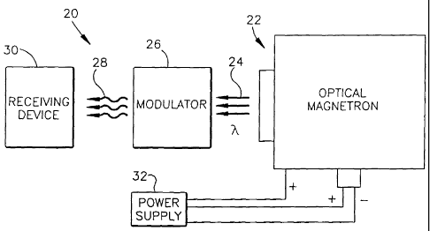
Referring initially to Fig. 1, an optical communication system 20 is shown.
In accordance with the present invention, the optical communication system 20
includes an optical magnetron 22. The optical magnetron 22 serves as a high-
efficiency source of output light which may be used to communicate information
optically from point-to-point. Although the optical magnetron 22 is described
herein in the context of its use in an optical communication system 20, it
will be
appreciated that the optical magnetron 22 has utility in a variety of other
applications. The present invention contemplates any and all such
applications.
As is shown in Fig. 1, the optical magnetron 22 serves to output optical
radiation 24 such as coherent light in the infrared, ultraviolet or visible
light region,
for example. The optical radiation is preferably radiation which has a
wavelength
corresponding to a frequency of 100 Ghz or more. In a more particular
embodiment, the optical magnetron 22 outputs optical radiation having a
wavelength in the range of about 10 microns to about 0.5 micron. According to
an even more particular embodiment, the optical magnetron outputs optical
radiation having a wavelength in the range of about 3.5 microns to about 1.5
microns.
The optical radiation 24 produced by the optical magnetron 22 passes
through a modulator 26 which serves to modulate the radiation 24 using known
CA 02381265 2002-O1-29
WO 01/97250 PCT/USO1/16622
techniques. For example, the modulator 26 may be an optical shutter which is
computer controlled based on data to be communicated. The radiation 24 is
selectively transmitted by the modulator 26 as modulated radiation 28. A
receiving device 30 receives and subsequently demodulates the modulated
radiation 28 in order to obtain the transmitted data.
The communication system 20 further includes a power supply 32 for
providing an operating do voltage to the optical magnetron 22. As will be
explained in more detail below, the optical magnetron 22 operates on a do
voltage
provided between the cathode and anode. In an exemplary embodiment, the
operating voltage is on the order of 30 kilovolts (kV) to 50 kV. However, it
will be
appreciated that other operating voltages are also possible.
Referring now to Figs. 2 and 3, a first embodiment of the optical magnetron
22 is shown. The magnetron 22 includes a cylindrically shaped cathode 40
having a radius rc. Included at the respective ends of the cathode 40 are
endcaps 41. The cathode 40 is enclosed within a hollow-cylindrical shaped
anode 42 which is aligned coaxially with the cathode 40. The anode 42 has an
inner radius ra which is greater than rc so as to define an interaction region
or
anode-cathode space 44 between an outer surface 48 of the cathode 40 and an
inner surface 50 of the anode 42.
Terminals 52 and 54 respectively pass through an insulator 55 and are
electrically connected to the cathode 40 to supply power to heat the cathode
40
and also to supply a negative (-) high voltage to the cathode 40. The anode 42
is
electrically connected to the positive (+) or ground terminal of the high
voltage
supply via terminal 56. During operation, the power supply 32 (Fig. 1 )
applies
heater current to and from the cathode 40 via terminals 52 and 54.
Simultaneously, the power supply 32 applies a do voltage to the cathode 40 and
anode 42 via terminals 54 and 56. The do voltage produces a do electric field
E
which extends radially between the cathode 40 and anode 42 throughout the
anode-cathode space 44.
The optical magnetron 22 further includes a pair of magnets 58 and 60
located at the respective ends of the anode 42. The magnets 58 and 60 are
11
CA 02381265 2002-O1-29
WO 01/97250 PCT/USO1/16622
configured to provide a do magnetic field B in an axial direction which is
normal to
the electric field E throughout the anode-cathode space 44. As is shown in
Fig. 3,
the magnetic field B is into the page within the anode-cathode space 44. The
magnets 58 and 60 in the exemplary embodiment are permanent magnets which
produce a magnetic field B on the order of 2 kilogauss, for example. Other
means for producing a magnetic field may be used instead (e.g., an
electromagnet) as will be appreciated. However, one or more permanent
magnets 58 and 60 are preferred particularly in the case where it is desirable
that
the optical magnetron 22 provide some degree of portability, for example.
The crossed magnetic field B and electric field E influence electrons
emitted from the cathode 40 to move in curved paths through the anode-cathode
space 44. With a sufficient do magnetic field B, the electrons will not arrive
at the
anode 42, but return instead to the cathode 40.
As will be described in more detail below in connection with Figs. 4a-4c, for
example, the inner surface 50 of the anode 42 includes a plurality of resonant
cavities distributed along the circumference. In a preferred embodiment, the
resonant cavities are formed by an even number of equally spaced slots which
extend in the axial direction. As the electrons emitted from the cathode 40
follow
the aforementioned curved paths through the anode-cathode space 44 and pass
in close proximity to the openings of these resonant cavities, a resonant
field is
created within the resonant cavities. More specifically, the electrons emitted
from
the cathode 40 tend to form a rotating electron cloud which passes in close
proximity to the resonant cavities. The electron cloud excites electromagnetic
fields in the resonant cavities causing them to oscillate or "ring". These
persistent
oscillatory fields in turn accelerate or decelerate passing electrons causing
the
electron cloud to bunch and form rotating spokes of charge.
Such operation involving a cathode, anode, crossed electric and magnetic
fields, and resonant cavities is generally known in connection with
conventional
magnetrons operating at frequencies below 100 Ghz. As noted above, however,
higher frequency operation has not been practical in the past for a variety of
reasons. The present invention overcomes such shortcomings by presenting a
12
CA 02381265 2002-O1-29
WO 01/97250 PCT/USO1/16622
practical device for operating at frequencies higher than 100 Ghz. Unlike
conventional magnetrons, the present invention is not limited to a small
number of
resonant cavities through which to generate the desired output radiation.
Moreover, the present invention is not constrained to a very small device
which
would require extremely high magnetic fields and power densities within the
device.
More particularly, the optical magnetron 22 includes a relatively large
number of resonant cavities within the anode 42. These resonant cavities are
preferably formed using high precision techniques such as photolithography,
micromachining, electron beam lithography, reactive ion etching, etc., as will
be
described more fully below. The magnetron 22 has a relatively large anode 42
compared to the operating wavelength A, such that the circumference of the
inner
anode surface 50, equal to 2 rr ra, is substantially larger than the operating
wavelength A. The result is an optical magnetron 22 which is practical both in
the
sense that it does not require extremely high magnetic fields and it can be
the
same size as a conventional magnetron used in the microwave band, for
example.
In the exemplary embodiment of Fig. 2, every other resonant cavity
includes a coupling port 64 which serves to couple energy from the respective
resonant cavities to a common resonant cavity 66. The coupling ports 64 are
formed by holes or slots provided through the wall of the anode 42. The
resonant
cavity 66 is formed around the outer circumference of the anode 42, and is
defined by the outer surface 68 of the anode 42 and a cavity defining wall 70
formed within a resonant cavity structure 72. As is shown in Figs. 2 and 3,
the
resonant cavity structure 72 forms a cylindrical sleeve which fits around the
anode
42. The resonant cavity 66 is positioned so as to be aligned with the coupling
ports 64 from the respective resonant cavities. The resonant cavity 66 serves
to
constrain the plurality of resonant cavities to operate in the pi-mode as is
discussed more fully below in connection with Fig. 4c.
13
CA 02381265 2002-O1-29
WO 01/97250 PCT/USO1/16622
In addition, the cavity structure 72 may serve to provide structural support
to the anode 42 which in many instances will be very thin. The cavity
structure 72
also facilitates cooling the anode 42 in the event of high temperature
operation.
The common resonant cavity 66 includes at least one or more output ports
74 which serve to couple energy from the resonant cavity 66 out through a
transparent output window 76 as output optical radiation 24. The output ports)
72 are formed by holes or slots provided through the wall of the resonant
cavity
structure 72.
The structure shown in Figs. 2 and 3, together with the other embodiment
described herein, is preferably constructed such that the anode-cathode space
44
and resonant cavity 66 are maintained within a vacuum. This prevents dust or
debris from entering into the device and otherwise disturbing the operation
thereof.
Fig. 4a represents a cross-sectional view of a portion of the anode 42
according to a general embodiment. The cross-section is taken in a plane which
is perpendicular to the common axis of the anode 42 and cathode 40 as will be
appreciated. The curvature of the anode 42 has not been shown for ease of
illustration. As is shown, each resonant cavity within the anode 42 is
represented
by a slot 80 formed at the surface 50 of the anode 42. In the exemplary
embodiment, the slots 80 have a depth d equal to J~/4 to allow for resonance,
where A represents the wavelength of the output optical radiation 24 at the
desired operating frequency. The slots 80 are spaced apart a distance of ~/2
or
less, and each slot has a width w equal to 118 or less. The slot width w
should be
~/8 or less to allow electrons to pass the slot 80 before the electric field
reverses
in pi-mode operation as can be shown.
The total number N of slots 80 in the anode 42 is selected such that the
electrons moving through the anode-cathode space 44 preferably are moving
substantially slower than the speed of light c (e.g., approximately on the
order of
0.1c to 0.3c). The slots 80 are evenly spaced around the inner circumference
of
the anode 42, and the total number N is selected so as to be an even number in
order to permit pi-mode operation. The slots 80 have a length which may be
14
CA 02381265 2002-O1-29
WO 01/97250 PCT/USO1/16622
somewhat arbitrary, but preferably is similar in length to the cathode 40. For
ease
of description, the N slots 80 may be considered as being numbered in sequence
from 1 to N about the circumference of the anode 42.
Fig. 4b represents a particular embodiment of the anode 42 designed to
encourage pi-mode oscillation at the desired operating frequency. The
aforementioned slots 80 are actually comprised of long slots 80a and short
slots
80b. The long slots 80a and short slots 80b are arranged at intervals of A/4
in
alternating fashion as shown in Fig. 4b. The long slots 80a and short slots
80b
have a depth ratio of 2:1 and an average depth of A/4 in the preferred
embodiment. Consequently, the long slots 80a have a depth dl equal to A/3 and
the short slots 80b have a depth ds equal to A/6. Such arrangement of long and
short slots is known in the microwave bands as a "rising sun" configuration.
Such
configuration promotes pi-mode oscillation with the long slots 80a lagging in
phase and the short slots 80b leading in phase.
Although not shown ~in Figs. 4a and 4b, one or more of the resonant
cavities formed by the respective slots 80 will include one or more coupling
ports
64 which couple energy from within the slot 80 to the common resonant cavity
66
as represented in Figs. 2 and 3, for example. Alternatively, the coupling
ports)
64 serve to couple energy from within the respective slots 80 directly out
through
the output window 76 as discussed below in connection with the embodiment of
Figs. 9 and 10, for example. The coupling ports 64 preferably are provided
with
respect to slots 80 which are in phase with each other so as to add
constructively.
Alternatively, one or more phase shifters may be used to adjust the phase of
radiation from the coupling ports 64 so as to all be in phase.
Fig. 4c represents another particular embodiment of the anode 42
designed to encourage pi-mode oscillation at the desired operating frequency.
Such embodiment of the anode 42 is specifically represented in the embodiment
of Figs. 2 and 3. An external stabilizing resonator in the form of the common
resonant cavity 66 serves to encourage pi-mode oscillation in accordance with
the
invention. Specifically, every other slot 80 (i.e., either every even-numbered
slot
or every odd-numbered slot) is coupled to the resonant cavity 66 via a
respective
CA 02381265 2002-O1-29
WO 01/97250 PCT/USO1/16622
coupling port 64 so as to all be in phase. The slots 80 are spaced at
intervals of
A/2 and otherwise each has a depth d equal to ~/4.
As will be appreciated, the slots 80 in each of the embodiments described
herein represent micro resonators. The following table provides exemplary
dimensions, etc. for an optical magnetron 22 in accordance with the present
invention. In the case of a practical sized device in which the cathode 40 has
a
radius rc of 2 millimeters (mm) and the anode 42 has an inner radius ra of 7
mm,
a length of 1 centimeter (cm), a magnetic field B of 2 kilogauss, an electric
field E
potential of 30 kV to 50 kV, the dimensions relating to the slots 80 in the
case of
the configuration of Fig. 4c may be as follows, for example:
Table:
Operating WavelengthNumber of SlotsSlot Width w Slot Depth d
~ (mm) N (microns) (microns)
10-2 87,964 1.25 2.5
3.5 x10'3 251,324 0.4375 0.875
1.5 x 10⁻³ 586,424 0.1875 0.375
0.5 x10⁻³ 1,759,274 0.0625 0.125
The output power for such a magnetron 22 will be on the order of 1 kilowatt
(kW) continuous, and 1 megawatt (MW) pulsed. In addition, efficiencies will be
on the order of 85%. Consequently, the magnetron 22 of the present invention
is
well suited for any application which utilizes a high efficiency, high power
output
such as communications, lighting, manufacturing, etc.
The micro resonators or resonant cavities formed by the slots 80 can be
manufactured using a variety of different techniques available from the
semiconductor manufacturing industry. For example, existing micromachining
techniques are suitable for forming slots having a width of 2.5 microns or so.
Although specific manufacturing techniques are described below, it will be
generally appreciated that an electrically conductive hollow cylinder anode
body
16
CA 02381265 2002-O1-29
WO 01/97250 PCT/USO1/16622
may be controllably etched via a laser beam to produce slots 80 having the
desired width and depth. Alternatively, photolithographic techniques may be
used
in which the anode 42 is formed by a succession of electrically conductive
layers
stacked upon one another with teeth representing the slots 80. For higher
frequency applications (e.g., A = 0.5 x 10⁻⁴ mm), electron beam (e-beam)
techniques used in semiconductor processing may be used to form the slots 80
within the anode 42. In its broadest sense, however, the present invention is
not
limited to any particular method of manufacture.
Referring now to Fig. 5, another embodiment of the optical magnetron in
accordance with the present invention is generally designated 22a. Such
embodiment is virtually identical to the embodiment of Figs. 2 and 3 with the
following exception. The common resonant cavity 66 in this embodiment has a
curved outer wall 70 so as to form a toroidal shaped resonant cavity 66. The
radius of curvature of the outer wall 70 is on the order of 2.0 cm to 2.0 m,
depending on the operating frequency. The toroidal shaped resonant cavity 66
serves to improve the ability of the common resonant cavity 66 to control the
pi-
mode oscillations at the desired operating frequency.
It is noted that each of the coupling ports 64 from the even numbered slots
80, for example, are aligned horizontally at the center of the anode 42 with
the
vertex of the curved outer wall 70. This tends to focus the resonant optical
radiation towards the center of the anode 42 and reduce light leakage from the
ends of the cylindrical anode 42. The odd numbered slots 80 do not include
such
coupling ports 64 and consequently are driven to oscillate out of phase with
the
even numbered slots 80.
Fig. 6 illustrates another embodiment of the optical magnetron which is
generally designated 22b. The embodiment of Fig. 6 is virtually identical to
that of
Fig. 5 with the following exceptions. In this particular embodiment, the
magnetron
22b comprises a double toroidal common resonator. More specifically, the
magnetron 22b includes a first toroidal shaped resonant cavity 66a and a
second
toroidal shaped resonant cavity 66b formed in the resonant cavity structure
72.
Each of the even-numbered slots 80 among the N total slots 80 is coupled by a
17
CA 02381265 2002-O1-29
WO 01/97250 PCT/USO1/16622
coupling port 64a to the first cavity 66a. Each of the odd-numbered slots 80
among the N total slots 80 is coupled to the second cavity 66b by way of a
coupling port 64b.
The first resonant cavity 66a is a higher frequency resonator designed to
lock a resonant mode at a frequency which is slightly higher than the desired
operating frequency. The second resonant cavity 66b is a Power frequency
resonator designed to lock a resonant mode at a frequency which is slightly
lower
than the desired frequency, such that the entire device oscillates at an
intermediate average frequency corresponding to the desired operating
frequency. The higher frequency modes within the first resonant cavity 66a
will
tend to lead in phase while the low frequency modes in the second resonant
cavity 66b lag in phase about the desired operation frequency. Consequently,
pi-
mode operation will result.
Output radiation 24 may be provided from one or both of the output ports)
74a and 74(b). Since the outputs from both will be out of phase with respect
to
each other, it may be desirable to include a phase shifter (not shown) for one
of
the output ports) 74a and 74b.
As in the previous embodiment, the radii of curvature for the outer walls
70a and 70b of the cavities 66a and 66b, respectively, are on the order of 2.0
cm
to 2.0 m. However, the radius of curvatures are designed slightly shorter and
longer for the walls 70a and 70b, respectively, in order to provide the
desired
highllow frequency operation with respect to the desired operating frequency.
In a different embodiment, more than two resonant cavities 66 may be
formed around the anode 42 for constraining operation to the pi-mode. The
present invention is not necessarily limited to a particular number.
Furthermore,
the cavities 66a and 66b in the embodiment of Fig. 6 may instead be designed
to
both operate at the desired operating frequency rather than offset as
previously
described and as will be appreciated.
Turning now to Figs. 7a and 7b, still another embodiment of an optical
magnetron is shown, this time designated as 22c. This embodiment illustrates
how every other slot 80 (i.e., all the even numbered slots or all the odd
numbered
18
CA 02381265 2002-O1-29
WO 01/97250 PCT/USO1/16622
slots) may include more than one coupling port 64 to couple energy from the
respective resonant cavity to the common resonant cavity 66. For example, Fig.
7a illustrates how even numbered slots 80 formed in the anode 42 alternate
having three and four coupling ports 64 in the respective slots 80. As in the
other
embodiments, the coupling ports 64 couple energy to the common resonant
cavity 66 in order to better control the oscillation modes and induce pi-mode
operation. As is also shown in Figs. 7a and 7b, the optical magnetron 22c may
include multiple output ports 74a, 74b, 74c, etc. for coupling the output
optical
radiation 24 from the resonant cavity 66 out through the output window 76. By
forming an array of output ports 74 and/or coupling ports 64 as described
herein,
it is possible to control the amount of coupling which occurs as will be
appreciated.
Although not shown in Fig. 7a, it will be appreciated that the common
resonant cavity 66 could be replaced with a toroidal shaped cavity as in the
embodiment of Fig. 5, for example. Moreover, it will be readily appreciated
that
an optical magnetron 22 in accordance with the invention may be constructed by
any combination of the various features and embodiments described herein,
namely (i) an anode structure comprising a plurality of small resonant
cavities 80
which may be scaled according to the desired operating wavelength to sizes as
small as optical wavelengths; (ii) a structure for constraining the resonant
cavities
80 to operate in the so-called pi-mode whereby each resonant cavity 80 is
constrained to oscillate pi-radians out of phase with its nearest neighbors;
and (iii)
means for coupling the optical radiation from the resonant cavities to deliver
useful output power. Different slot 80 configurations are discussed herein, as
are
different forms of one or more common resonant cavities for constraining the
resonant cavities. In addition, the description herein provides means for
coupling
power from the resonant cavities via the various forms and arrangements of
coupling ports 64 and output ports 74. On the other hand, the present
invention
is not intended to be limited in its broadest sense to the particular
configurations
described herein.
19
CA 02381265 2002-O1-29
WO 01/97250 PCT/USO1/16622
Referring briefly to Fig. 8, a vertically stacked multifrequency embodiment
of the present invention is shown. In this embodiment, the anode 42 is divided
into an upper anode 42a and a lower anode 42b. In the upper anode 42a, the
slots 80a are designed with a width, spacing and number corresponding to a
first
operative wavelength A,. The slots 80b in the lower anode 42b, on the other
hand, are designed with a width, spacing and number corresponding to a second
operating wavelength l~~ different from the first operating wavelength J~,.
Even-numbered slots 80a, for example, in the upper anode 42a include
coupling ports 64a which couple energy from a rotating electron cloud formed
in
the upper anode 42a to an upper common resonant cavity 66a. Likewise, even-
numbered (or odd numbered) slots 80b in the lower anode 42b include coupling
ports 64b which couple energy from a rotating electron cloud formed in the
lower
anode 42b to a lower common resonant cavity 66b. The upper and lower
common resonant cavities 66a and 66b serve to promote pi-mode oscillation at
the respective frequencies A~ and A2 in the upper and lower anodes 42a and
42b.
Energy from the common resonant cavities 66a and 66b is output through the
output window 76 via one or more output ports 74a and 74b, respectively.
Thus, the present invention as represented in Fig. 8 provides a manner for
vertically stacking two or more anode resonators each having a different
operating
wavelength (e.g., A~ and A2). The anodes (e.g., upper and lower anodes 42a and
42b) may be stacked vertically between a single pair of magnets 58 and 60. The
stacked device may therefore emit multiple frequencies. For example, in a
magnetron operating at visible light frequencies, anode resonators oscillating
at
red, green and blue wavelengths may be stacked vertically in a single device.
The light outputs may be utilized separately as part of a color display or
combined, for example, to produce a white light source.
Figs. 9 and 10 illustrate an embodiment of the invention which provides
direct output coupling via the coupling ports 64 through the output window 76.
Fig. 10 illustrates how the rotating electron cloud within the anode-cathode
space
44 creates fringing fields 90 at the opening of the slots 80 and the coupling
ports
64 therein as the cloud passes by. The fringing fields 90 at the openings of
the
CA 02381265 2002-O1-29
WO 01/97250 PCT/USO1/16622
coupling ports are emitted from the opposite side of the anode 42 as output
radiation fields 92.
Fig. 9 illustrates an embodiment in which the output radiation fields 92, as
represented in Fig. 10, are output directly through the output window 76. In
the
other embodiments described herein, the radiation through the coupling ports
64
is first introduced into a common resonant cavity 66 in the same manner
represented in Fig. 10. The common resonant cavity 66 provides improved
control of the pi-mode operation as previously discussed. Nevertheless, the
present invention contemplates an embodiment which is perhaps less efficient
but
also useful in which the coupling ports 64 provide output radiation directly
to the
output window 76. In such case, as is shown in Fig. 9, there is no need for
coupling ports 64 in the slots 80 other than those which direct output
radiation
toward the output window 76. The coupling principles of Fig. 10, however,
apply
to all of the coupling ports 64 and output ports 74 discussed herein as will
be
appreciated.
Figs. 11 a-11 c illustrate an embodiment of an optical magnetron 22e
designed for operation in the TEM2o mode in accordance with the present
a
invention. The embodiment is similar to that described above in connection
with
Fig. 5 in that it includes a toroidal shaped resonant cavity 66 with a curved
outer
wall 70. The embodiment differs from that of Fig. 5 in that even numbered
slots .
80 have a single coupling port 64a which is aligned with vertex of the curved
outer
wall 70 as is shown in Fig. 11 b. Consequently, the even numbered slots 80
tend
to excite the central spot 100 of the resonant cavity 66. On the other hand,
the odd numbered slots 80 include two coupling ports 64b and 64c offset
vertically on opposite sides of the vertex of the curved outer wall 70 as is
shown in
Fig. 11 c. Consequently, the odd numbered slots 80 will tend to excite outer
spots
102 of the resonant cavity 66. The result is a TEM2o single mode within the
toroidal shaped resonant cavity 66. The central spot 100 has an electric field
direction (e.g., out of the page in Figs. 11 b and 11 c) which is opposite the
electric
field direction (e.g., into the page) of the outer spots 102. The electric
fields
change direction each half-cycle of the oscillation. The even-numbered slots
80
21
CA 02381265 2002-O1-29
WO 01/97250 PCT/USO1/16622
will thus have their electric fields driven out-of-phase with respect to the
odd-
numbered slots 80, and the slots 80 are forced to operate in the desired pi-
mode.
Figs. 11d-11f represent an embodiment of an optical magnetron 22f which,
in this case, is designed for operation in the TEM~o mode according to the
present
invention. Again, the embodiment is similar to that described above in
connection
with Fig. 5 in that it includes a toroidal shaped resonant cavity 66 with a
curved
outer wall 70. This embodiment differs from that of Fig. 5 in that even
numbered
slots 80 have a coupling port 64a which is offset above the vertex of the
curved
outer wall 70 as shown in Fig. 11 e. As a result, the even numbered slots 80
tend
to excite an upper spot 104 of the resonant cavity 66.
The odd numbered slots 80, conversely, include a coupling port 64b which
is offset below the vertex of the curved outer wall 70 as is shown in Fig.
11f. As a
result, the odd numbered slots 80 tend to excite a lower spot 106 of the
resonant
cavity 66. In this case, the result is a TEM~o single mode within the toroidal
shaped resonant cavity 66. The upper spot 104 has an electric field direction
(e.g., into the page in Figs. 11 a and 11 f) which is opposite the electric
field
direction (e.g., out of the page) of the lower spot 106. A small protrusion
108, or
"spoiler" may be provided around the circumference of the resonant cavity 66
at
the vertex of the curved outer wall 70 to help suppress the TEMoo mode. The
respective electric fields of the upper and lower spots change direction each
half-
cycle of the oscillation. The even numbered slots 80 thus have their electric
fields
driven out-of phase with respect to the odd numbered slots 80, and the slots
80
are forced to operate in the desired pi-mode.
Figs. 11a-11f present two possible single modes in accordance with the
present invention. It will be appreciated, however, that other TEM modes may
also be used for pi-mode control without departing from the scope of the
invention.
As far as manufacture, the cathode 40 of the magnetron 22 may be formed
of any of a variety of electrically conductive metals as will be appreciated.
The
cathode 40 may be solid or simply plated with an electrically conductive metal
such as copper, gold or silver, or may be fabricated from a spiral wound
thoriated
22
CA 02381265 2002-O1-29
WO 01/97250 PCT/USO1/16622
tungsten filament, for example. Alternatively, a cold field emission cathode
40
which is constructed from micro structures such as carbon nanotubes may also
be used.
The anode 42 is made of an electrically conductive metal and/or of a non-
conductive material plated with a conductive layer such as copper, gold or
silver.
The resonant cavity structure 72 may or may not be electrically conductive,
with
the exception of the walls of the resonant cavity or cavities 66 and output
ports 74
which are either plated or formed with an electrically conductive material
such as
copper, gold or silver. The anode 42 and resonant cavity structure 72 may be
formed separately or as a single integral piece as will be appreciated.
Figs. 12a and 12b illustrate an exemplary manner for producing an anode
42 using an electron beam Lithography approach. A cylindrical hollow aluminum
rod 110 is selected having a radius equal to the desired inner radius ra of
the
anode 42. A layer 112 of positive photoresist, for example, is formed about
the
circumference of the rod 110 as is shown in Fig. 12a. The length I of the
resist
layer 112 along the axis of the rod 110 should be made on the order of the
desired length of the anode 42 (e.g., 1 centimeter (cm) to 2 cm). The
thickness of
the of the resist layer 112 is controlled so as to equal the desired depth of
the
resonant cavities or slots 80.
The rod 110 is then placed in a jig 114 within an electron beam patterning
apparatus used for manufacturing semiconductors, for example, as is
represented in Fig. 12b. An electron beam 116 is then controlled so as to
pattern
by exposure individual lines along the length of the of the resist layer 112
parallel
with the axis of the rod 110. As wilt be appreciated, these lines will serve
to form
the sides of the resonant cavities or slots 80 in the anode 42. The lines are
controlled so as to have a width equal to the spacing between adjacent slots
80
(e.g., the quantity J~/2-A/8 in the case of the embodiments such as Fig. 4a
and Fig.
4c). The lines are spaced apart from each other by the desired width w of the
slots 80 (e.g., ~/8 in the case of embodiments such as Fig. 4a and Fig. 4c).
The patterned resist layer 112 is then developed and etched such that the
exposed portion of the resist layer 112 is removed. This results in the rod
110
23
CA 02381265 2002-O1-29
WO 01/97250 PCT/USO1/16622
having several small fins or vanes, formed from resist, respectively
corresponding
to the slots 80 which are to be formed in the anode 42. The rod 110 and the
corresponding fins or vanes are then copper electroplated to a thickness
corresponding to the desired outer diameter of the anode 42 (e.g., 2 mm). As
will
be appreciated, the copper plating will form around the fins or vanes until
the
plating ultimately covers the rod 110 substantially uniformly.
The aluminum rod 110 and fins or vanes made of resist are then removed
from the copper plating by chemically dissolving the aluminum and resist with
any
available solvent known to be selective between aluminum/resist and copper.
Similar to the technique known as lost wax casting, the remaining copper
plating
forms an anode 42 with the desired resonant cavities or slots 80.
1t will be appreciated that the equivalent structure may be formed via the
same techniques except with a negative photoresist and forming an inverse
pattern for the slots, etc.
Slots 80 having different depths, such as in the embodiment of Fig. 4b,
may be formed using the same technique but with multiple layers of resist. A
first
layer of resist 112 is patterned and etched to form the fins or vanes on the
aluminum rod 110 corresponding to both the long slots 80a and the short slots
80b (Fig. 4b). The first layer of resist 112 has a thickness ds corresponding
to the
depth of the short slots. A second and subsequent layer of resist 112 is
formed
on the first patterned layer. The second layer 112 is patterned to form the
remaining portion of the fins or vanes which will be used to form the long
slots 80.
In other words, the second layer 112 has a thickness of dl -ds. The various
coupling ports 64 may be formed in the same manner, that is with additional
layers of resist 112 in order to define the coupling ports 64 at the desired
locations. The rod 110 and resist is then copper plated, for example, to form
the
anode 42 with the rod 110 and resist subsequently being dissolved away. The
same technique for forming the coupling ports 64 may be applied to the above-
described manufacturing technique for the embodiment of Fig. 4c, as will be
appreciated.
24
CA 02381265 2002-O1-29
WO 01/97250 PCT/USO1/16622
Fig. 13 illustrates the manner in which the anode 42 may be formed as a
vertical stack of layers using known micromachining/photolithography
techniques.
A first layer of metal such as copper is formed on a substrate. A layer of
photoresist is then formed on the copper and thereafter the copper is
patterned
and etched (e.g., via electron beam) so as to define the resonant cavities or
slots
80 in a plane normal to the axis of the anode 42. Subsequent layers of copper
are then formed and etched atop the original layers in order to create a stack
which is subsequently the desired length of the anode 42. As will be
appreciated,
planarization layers of oxide or some other material may be formed in between
copper layers and subsequently removed in order to avoid filling an existing
slot
80 when depositing a subsequent layer of copper, for example. Also, such oxide
may be used to define coupling ports 64 as desired, such oxide subsequently
being removed by a selective oxide/copper etch.
As will be appreciated, known photolithography and micromachining
techniques used in the production of semiconductor devices may be used to
obtain the desired resolution for the anode 42 and corresponding resonant
cavities (e.g., slots 80). The present invention nevertheless is not intended
to be
limited, in its broadest sense, to the particular methods described herein.
Figs. 14a-14c illustrate a technique for forming the resonant cavity
structure 72 with a toroidal shape as described herein. For example, an
aluminum rod 120 is machined so as to have bump 122 in the middle as shown in
Fig. 14a. The radius of the rod 120 in upper and lower portions 124 is set
equal
to approximately the outer radius of the anode 42 around which the structure
72
will fit. The bump 122 is machined so as to have a radius corresponding to the
vertex point of the structure 72 to be formed.
Thereafter, the bump 122 is rounded to define the curved toroidal shape of
the wall 70 as described above. Next, the thus machined rod 112 is
electroplated
with copper to form the structure 72 therearound as represented in Fig. 14b.
The
aluminum rod 120 is then chemically dissolved away from the copper structure
72
so as to result in the structure 72 as shown in Fig. 14c. Output ports 74 may
be
formed as needed using micromachining (e.g., via laser milling), for example.
CA 02381265 2002-O1-29
WO 01/97250 PCT/USO1/16622
Reference is now made to Figs. 15-38 which relate to a variety of different
anode structures 42 suitable for use in alternative embodiments of an optical
magnetron in accordance with the present invention. As will be appreciated,
the
anodes 42 as shown in Figs. 15-38 can be substituted for the anode 42 in the
other embodiments previously discussed herein, for example the embodiments of
Figs. 5-9. Again, each of the anodes 42 has a generally hollow-cylindrical
shape
with an inner surface 50 defining the anode-cathode space into which the
cathode
40 (not shown) is coaxially placed. Depending on the particular embodiment,
one
or more common resonant cavities 66 (not shown) are formed around the outer
circumference of the anode 42 via a resonant cavity structure 72 (also not
shown)
as in the previous embodiments. Since only the structure of the anode 42
itself
differs in relevant part with respect to the various embodiments discussed
herein,
the following discussion is limited to the anode 42 for sake of brevity. It
will be
appreciated by those skilled in the art that the present invention
contemplates an
optical magnetron as previously discussed herein incorporating any and all of
the
different anode structures 42. Moreover, it will be appreciated that the anode
structures 42 may have utility as part of a magnetron in bandwidths outside of
the
optical range, and are considered part of the invention.
In particular, Figs. 15-18 represent an anode 42 in accordance with an
alternate embodiment of the present invention. As is shown in Fig. 15, the
anode
42 has a hollow-cylindrical shape with an inner surface 50 and an outer
surface
68. Like the previous embodiments discussed above, a plurality N (where N is
an
even number) of slots or cavities 80 are formed along the inner surface 50.
Again, the slots 80 serve as resonant cavities. The number and dimensions of
the slots or cavities 80 depends on the desired operating wavelength A as
discussed above. The anode 42 is formed by a plurality of pie-shaped wedge
elements 150, referred to herein simply as wedges. When stacked side by side,
the wedges 150 form the structure of the anode 42 as shown in Fig. 15.
Fig. 16 is a top view of an exemplary wedge 150. Each wedge 150 has an
angular width ~ equal to (2rr/N) radians, and an inner radius of ra equal to
the
inner radius ra of the anode 42. The outer radius ro of the wedge 150
26
CA 02381265 2002-O1-29
WO 01/97250 PCT/USO1/16622
corresponds to the outer radius ro of the anode 42 (i.e., the radial distance
to the
outer surface 68. Each wedge 150 further includes a recess 152 formed along
the apex of the wedge 150 which defines, in combination with the side wall 154
of
an adjacent wedge 150, one of the N resonant cavities 80.
As is shown in Fig. 16, each recess 152 has a length equal to d, which is
equal to the depth of each resonant cavity 80. In addition, each recess 152
has a
width w which is equal to the width of each resonant cavity 80. Thus, when
stacked together side-by-side, the wedges 150 form N resonant cavities 80
around the inner surface 50 of the anode 42. The number N, depth, width and
spacing therebetween of resonant cavities 80 is selected based on the desired
operating wavelength as discussed above, and the dimensions of the wedges 150
are selected accordingly. The length L of each wedge 150 (see, e.g., Fig. 17),
is
set equal to the desired height of the anode 42 as will be appreciated.
As in the embodiments discussed above, the wedges 150 may be
nominally considered as even and odd-numbered wedges 150 arranged about
the circumference of the anode 42. The even-numbered wedges 150 include a
recess 152 to produce even-numbered cavities 80 and the odd-numbered
wedges 150 include a recess 152 which produces odd-numbered cavities 80.
Figs. 17 and 18 show the front sides of even and odd-numbered wedges 150a
and 150b, respectively. The front sides of the even-numbered and odd-
numbered wedges 150a and 150b include a recess 152 as shown in Figs. 17 and
18, respectively. In addition, however, each of the odd-numbered wedges 150b
include a coupling port recess 164 as shown in Fig. 18. Each coupling port
recess 164 in combination with the back side wall 154 of an adjacent wedge
150a
forms a coupling port 64 acting as a single mode waveguide which serves to
couple energy from the odd-numbered cavities 80 to a common resonant cavity
72. It is noted that only one of such coupling ports 64 is shown in Fig. 15 by
way
of example. As will be appreciated, the back side wall 154 of each wedge 150
is
substantially planar as is the front side wall 166 of each wedge 150. Thus,
the
recesses 152 and 164 combine with the back side wall 154 of an adjacent wedge
150 to form a desired resonant cavity 80 and coupling port 64.
27
CA 02381265 2002-O1-29
WO 01/97250 PCT/USO1/16622
The wedges 150 may be made from various types of electrically conductive
materials such as copper, aluminum, brass, etc., with plating (e.g., gold) if
desired. Alternatively, the wedges 150 may be made of some non-conductive
material which is plated with an electrically conductive material at least in
the
regions in which the resonant cavities 80 and coupling ports 64 are formed.
The wedges 150 may be formed using any of a variety of known
manufacturing or fabrication techniques. For example, the wedges 150 may be
machined using a precision milling machine. Alternatively, laser cutting
and/or
milling devices may be used to form the wedges. As another alternative,
lithographic techniques may be used to form the desired wedges. The use of
such wedges allows precision control of the respective dimensions as desired.
After the wedges 150 have been formed, they are arranged in proper order
(i.e., even-odd-even-odd...) to form the anode 42. The wedges 150 may be held
in place by a corresponding jig, and the wedges soldered, brazed or otherwise
bonded together to form an integral unit.
The embodiment of Figs. 15-18 is analogous to the embodiment of Fig. 5
in that only the even/odd numbered cavities 80 include a coupling port 64,
whereas the odd/even numbered cavities 80 do not include such a coupling port
64. The coupling of every other cavity 80 to the common resonant cavity 66
serves to induce pi-mode operation in the same manner.
Figs. 19-23 relate to another embodiment of an anode 42. Such
embodiment is generally similar insofar as wedge-based construction, and hence
only the differences will be discussed herein for sake of brevity. Fig. 19
illustrates
the anode 42 in schematic cross section. In this particular embodiment, each
resonant cavity 80 includes a coupling port or ports 64 each acting as a
single
mode waveguide for coupling energy between the resonant cavity 80 and one or
more common resonant cavities 66 in order to induce further pi-mode operation.
The coupling ports 64 formed by the odd-numbered wedges 150b introduce an
additional 1/2A delay in relation to the coupling ports 64 formed by the even-
numbered wedges 150a, so as to provide the appropriate phase relationship.
28
CA 02381265 2002-O1-29
WO 01/97250 PCT/USO1/16622
Fig. 19 illustrates how the odd-numbered wedges 150b in this particular
embodiment include a recess 164b which extend radially and at an angle in the
H-plane direction between the recess 152 which forms the corresponding
resonant cavity 80 and the outer surface 68 of the anode 42. The even-
s numbered wedges 150a, on the other hand, each include a pair of recesses
164a
that each extend radialfy and perpendicular to the center axis between the
recess
152 which forms the corresponding resonant cavity 80 and the outer surface 68.
(It will be appreciated that the even-numbered wedge 150 as shown in Fig. 19
is
flipped with respect to its intended orientation in order to provide a clear
view of
the recesses 164a).
The angle at which the recesses 164b are formed in the odd numbered
wedges is selected so as each to introduce overall an additional 1/2A delay
compared to the recesses 164a. Thus, radiation which is coupled between the
resonant cavities 80 formed by the even and odd-numbered wedges 150 will have
the appropriate phase relationship with respect to the common resonant cavity
66.
Figs. 22 and 23 illustrate how the odd-numbered wedges 150b in the
embodiment of Fig. 19 alternate between upwardly directed and downwardly
directed angles. This allows for a more even distribution of the energy with
respect to the axial direction within the anode-cathode space and the common
resonant cavity 66 (not shown), as will be appreciated.
Figs. 24-27 illustrate another embodiment of the anode 42 using an H-
plane bend of the coupling ports 64 formed by the odd-numbered wedges to
introduce an additional ll2A delay relative to the coupling ports 64 formed by
the
even-numbered wedges. The even-numbered wedges 150a are similar to those
in the embodiment of Figs. 19-23. However, the odd-numbered wedges 150b
include a pair of recesses 164b each presented at an angle relative to the H-
plane. Each of the recesses 164b is designed to form a single mode waveguide
in combination with the back side wall 154 of an adjacent wedge 150a. The
recesses 164b are bent along the H-plane so as each to provide an additional
1/2A delay compared to the recesses 164a in the even-numbered wedges.
29
CA 02381265 2002-O1-29
WO 01/97250 PCT/USO1/16622
Consequently, the desired phase relationship between the resonant cavities 80
and one or more surrounding common resonant cavities 66 (not shown) is
provided for pi-mode operation. Moreover, because each of the recesses 164b
include a pair of bends 170 and 172, the coupling ports 64 formed by the
recesses are generally evenly distributed along the axial direction of the
anode
42. Thus, such an embodiment may be more favorable than the embodiment of
Figs. 19-23 which called for two different odd-numbered wedges 150b1 and
150b2. It will also be appreciated that again the even-numbered wedge 150a as
shown in Fig. 24 is flipped with respect to its intended orientation in order
to
provide a clear view of the recesses 164a.
Figs. 23 and 29 illustrate yet another embodiment of a wedge-based
construction of an anode 42. This embodiment differs from the embodiment of
Figs. 19-23 in the following manner. The even-numbered wedges 150a include
three recesses 164a rather than two. The odd-numbered wedges 150b1 and
150b2 include two recesses 164b rather than one. As will be appreciated, the
number of recesses 164 formed in the respective wedges 150 is not limited to
any
particular number in accordance with the present invention. The number of
recesses 164 may be selected based on the desired amount of coupling between
the anode-cathode space and the common resonant cavity or cavities 66, as wilt
be appreciated. It will again be appreciated that the even-numbered wedge 150a
as shown in Fig. 23 is flipped with respect to its intended orientation in
order to
provide a clear view of the recesses 164a.
Referring now to Figs. 30-33, yet another embodiment of an anode 42 is
presented which utilizes an additional 1/2A delay in the coupling ports 64
formed
by the even-numbered wedges 150a compared to the odd-numbered wedges
150b to induce pi-mode operation. In this embodiment, however, the additional
ll2A delay is provided by adjusting the relative width of the recesses 164 (as
compared to introducing an H-plane bend). More particularly, each odd-
numbered wedge 150b includes a pair of recesses 164b which combine with the
back side wall 154 of an adjacent wedge 150a to form single mode waveguides
serving as coupling ports 64. The even-numbered wedges 150a, on the other
CA 02381265 2002-O1-29
WO 01/97250 PCT/USO1/16622
hand, include recesses 164a which have a width 174 that is relatively wider
than
that of the recesses 164b. As is known from waveguide theory, an appropriately
selected wider width 174 of the recesses 164a may be chosen to provide for an
additional 1/2A delay compared to that of the recesses 164b. Thus, the desired
phase relationship between the coupling ports 64 formed by the odd-numbered
and even-numbered wedges may be obtained for pi-mode operation.
Figs. 34-38 relate to an embodiment of the anode 42 which utilizes bends
in the E-plane of the coupling ports 64 to provide the desired additional 1/2A
delay
for pi-mode operation. As is shown in Fig. 34, the anode 42 is made up of
several layers 180 stacked on top of each other with or without a spacer
member
(not shown) therebetween. The layers 180 are nominally referred to as either
an
even-numbered layer 180a or an odd-numbered layer 180b which alternate within
the stack. The even-numbered layers 180a include linear waveguides forming
coupling ports 64 which serve to couple energy between the anode-cathode
space and one or more common resonant cavities 66 (not shown). The odd-
numbered layers 180b include waveguides which are curved in the E-plane and
form coupling ports 64 which also serve to couple energy between the anode-
cathode space and the one or more common resonant cavities 66. The
waveguides in the odd-numbered layers 180b are curved so as to introduce an
additional 1/2A delay compared to the waveguides in the even-numbered layers
180a to provide the desired pi-mode operation.
Figs. 35 and 36 illustrate an exemplary even-numbered layer 180a. Each
layer 180a is made up of N/2 guide elements 182, where N is the desired number
of resonant cavities 80 as above. The guide elements 182 are each formed in
the
shape of a wedge as shown in Fig. 36. The guide elements 182 are arranged
side by side as shown in Fig. 35 to form a layer which defines the inner
surface
50 and outer surface 68 of the anode 42. The tip of each wedge includes a slot
which defines a resonant cavity 80 therein. In addition, adjacent guide
elements
182 are spaced apart so as to form a resonant cavity 80 therebetween as shown
in Fig. 36. As will be appreciated, the resonant cavities 80 formed in each of
the
layers 180 are to be aligned when the layers 180 are stacked together.
Aligning
31
CA 02381265 2002-O1-29
WO 01/97250 PCT/USO1/16622
holes or marks 184 may be provided in the elements 182 to aid in such
alignment
between layers.
As best shown in Fig. 36, the space between the guide elements 182
defines a radial tapered waveguide which serves as a coupling port 64 between
an even-numbered resonant cavity 80 and the outer surface 68 of the anode 42.
The thickness of the guide elements 182 is provided such that the coupling
ports
64 have an H-plane height corresponding to the desired operating wavelength A.
Similarly, the dimensions of the resonant cavities 80 and the spacing between
the
guide elements 182 are selected for the desired wavelength A.
The guide elements 182 are made of a conductive material such as
copper, polysilicon, etc. so as to define the conductive walls of the resonant
cavities and coupling ports 64. Alternatively, the guide elements 182 may be
made of a non-conductive material with conductive plating at least at the
portions
defining the walls of the resonant cavities and coupling ports 64.
A spacer element 186 (shown in part in Fig. 36) is formed between
adjacent layers 180 in the stack making up the anode 42. The spacer 186 is
conductive at least in relevant part to provide the conductive E-plane walls
of the
coupling ports 64 in the layers 180. The spacer 186 may be washer shaped with
an inner radius equal to the inner radius ra of the anode 42.
Figs. 37 and 38 illustrate an exemplary odd-numbered layer 180b. The
odd-numbered layer 180b is similar in construction to that of the even-
numbered
layer with the exception that the guide elements 182 are curved to provide a
desired bend in the E-plane direction of tapered waveguides forming the
coupling
ports 64. The particular radius of curvature of the bend is calculated to
provide
the desired additional 1/2A delay relative to the coupling ports 64 of the
even-
numbered layers 180a for pi-mode operation. Also, the coupling ports 64 in the
odd-numbered layers 180b serve to couple the odd-numbered resonant cavities
80 to the outer surface 68 of the anode 42, rather than the even-numbered
resonant cavities 80 as in the even-numbered layers 180a.
The embodiment of Figs. 34-38 is particularly well suited to known
photolithographic fabrication methods as will be appreciated. A large anode 42
32
CA 02381265 2002-O1-29
WO 01/97250 PCT/USO1/16622
may be built up from layers 180b of E-plane bends interposed between layers
180a of straight waveguides. The layers may be formed and built up using
photolithographic techniques. The appropriate dimensions for operation even at
higher optical wavelengths can be achieved with the desired resolution. The
guide elements 182 may be formed of copper or polysilicon, for example. The
waveguides forming the coupling ports 64 may be filled with a suitable
dielectric to
provide planarization between layers 180 if desired. The spacers 186 between
layers 180 may be formed of copper, polysilicon, etc., as will be appreciated.
In another embodiment, each of the layers 180 are generally identical with
coupling ports 64 leading from each of the resonant cavities 80 radially
outward to
the outer surface 68 of the anode. In this case, however, height of the
coupling
ports 64 corresponding to the odd-numbered resonant cavities 80 is greater
than
the height of the coupling ports 64 corresponding to the even-numbered
resonant
cavities 80. The difference in height corresponds to a difference in width as
discussed above in relation to the embodiment of Figs. 30-33, and is provided
so
as to produce the desired additional 112A delay relative to the coupling ports
64 of
the even-numbered resonant cavities 80 for pi-mode operation.
It will therefore be appreciated that the optical magnetron of the present
invention is suitable for operating at frequencies heretofore not possible
with
conventional magnetrons. The optical magnetron of the present invention is
capable of producing high efficiency, high power electromagnetic energy at
frequencies within the infrared and visible light bands, and which may extend
beyond into higher frequency bands such as ultraviolet, x-ray, etc. As a
result,
the optical magnetron of the present invention may serve as a light source in
a
variety of applications such as long distance optical communications,
commercial
and industrial lighting, manufacturing, etc.
Although the invention has been shown and described with respect to
certain preferred embodiments, it is obvious that equivalents and
modifications
will occur to others skilled in the art upon the reading and understanding of
the
specification. For example, although slots are provided as the simplest form
of
33
CA 02381265 2002-O1-29
WO 01/97250 PCT/USO1/16622
resonant cavity, other forms of resonant cavities may be used within the anode
without departing from the scope of the invention.
Furthermore, although the preferred techniques for providing pi-mode
operation have been described in detail, other techniques are also within the
scope of the invention. For example, cross coupling may be provided between
slots. The slots 80 are spaced by'/2 A, and coupling channels are provided
between adjacent slots 80. The coupling channels from slot to slot measure 3/2
. In another embodiment, a plurality of optical resonators are embedded around
the circumference of the anode structure with non-adjacent slots constrained
to
oscillate out of phase by coupling to a single oscillating mode in a
corresponding
one of the optical resonators. Other means will also be apparent based on the
description herein.
Additionally, it will be appreciated that the toroidal resonators described
herein which employ curved surfaces and TEM modes to control pi-mode
oscillation may be utilized in otherwise conventional magnetrons. More
specifically, the feature of the invention relating to a toroidal resonator
may be
used for controlling pi-mode oscillation in non-optical magnetrons such as
those
operating at microwave frequencies below 100 Ghz.
The present invention includes all such equivalents and modifications, and
is limited only by the scope of the following claims.
34