Note: Descriptions are shown in the official language in which they were submitted.
CA 02381311 2002-02-05
WO 01/14838 PCT/GBOO/03243
1
MICRO-BRIDGE STRUCTURE
This invention relates to a method of making a micro-bridge and a new
structure for a micro-bridge, such as may be used in imaging devices to
detect incident radiation. The invention arose from the field of thermal
imaging, but is not necessarily limited to that field.
Infra-red imaging cameras based on two-dimensional arrays of thermal
detectors are attractive due to their near ambient temperature operation.
Thermal detectors used for infra-red imaging rely on the temperature
change of the sensing material due to absorption of infra-red radiation. A
1 C temperature change in the scene leads to a temperature change of
about 0.001 C temperature change within the detector and it is therefore
important to try and maximise the amount of radiation absorbed.
The sensing material has a temperature dependant property which allows
the magnitude of the change in temperature to be detected, amplified and
displayed using electronic circuitry. Examples are pyroelectric arrays,
which rely on the change in electrical polarisation with temperature which
occurs in ferroelectric materials, and resistance micro-bolometer arrays
which utilise the change in electrical resistance with temperature which
occurs in some materials
In all types of thermal detector it is advantageous to maximise the rise in
temperature of the sensing material due to the absorption of infra-red
radiation. The temperature rise is reduced by any thermal conduction
mechanism which takes heat from the sensing material. This results in
detector designs which maximise the thermal isolation of the sensing
material. The requirements for electrical read-out and mechanical rigidity
mean that, for most practical detectors, a physical connection is required
WO 01/14838 CA 02381311 2002-02-05 PCT/GB00/03243
2
to the sensing material.
Infra-red (IR) imaging relies on the fact that all objects radiate energy
with a peak wavelength depending on their temperature. For ambient
temperature objects this peak wavelength is in the Infra-red at about
m. Hotter objects radiate more intensely. IR imaging typically
involves using lenses, which may be of Germanium, to collect and focus
this radiation onto an array of sensitive elements placed in the focal plane
of the optics. The elements are normally micro-capacitors or micro-
10 resistors (micro-bolometers) whose characteristic parameter (charge or
resistance respectively) depends on the temperature. The micro-
bolometers are usually formed on silicon substrates using "micro-
machining techniques". This involves depositing and lithographically
patterning an active layer over a sacrificial layer that is finally etched
away to leave a free-standing, thermally isolated structure.
Such a structure is shown in Figure 1 of the accompanying drawings
wherein legs 2, 4 support the main body of the element 1 above a
substrate (not shown). The legs 2, 4 ensure that mechanical support is
provided for the main body but with low thermal conductivity to the
substrate.
Each element generates an electric signal proportional to its temperature
that, in turn, depends on the intensity of the IR energy absorbed by it or
its adjacent layer. The electrical signals must then be read out using a
circuit that will both filter and amplify.
Traditionally the quantum devices used to detect IR radiation have
required cooling to liquid nitrogen temperatures. The "uncooled"
technology described herein operates at room temperatures. Since IR
WO 01/14838 CA 02381311 2002-02-05 PCT/GBOO/03243
3
radiation is not obscured by smoke this technology is also useful in fire-
fighting applications. There are also applications where it is not
necessary to form high-resolution images. The IR sensitive elements can
be used for simple "intruder detectors" or fire detectors.
Presently there are two basic forms of the resistance micro-bridge.
Firstly, there is the homogeneous bridge type, as shown in section in
Figure 2a of the accompanying drawings. In this type of bolometer the
bridge is formed from a material whose properties change as the
temperature changes through radiation being absorbed. The change in
material properties is determined in some manner, perhaps by measuring a
change in current passing through the bridge. The skilled person will
appreciate that whilst the homogeneous bridge can work satisfactorily well
its performance may not be as efficient as desired.
The second class of micro-bridge can be termed "film-on-support" and
provides a temperature dependent material (which may be resistive) as a
film above a supporting bridge. Such a film on support micro-bridge is
shown in section in Figure 2b of the accompanying drawings. The bridge
absorbs incident thermal radiation of the wavelengths of interest causing a
temperature change within the bridge which effects the resistance of the
resistive material. Generally the resistive material will be a metal which
when positioned above the bridge reflects some of the incident radiation
reducing the sensitivity of the micro-bolometer. Further, the provision of
the metal on top of the bridge requires vias to be fabricated through the
bridge necessitating further processing steps.
An example of a micro-bridge structure is shown in the Journal of
Microelectromechanical systems Vol.5 No. 4 December 1996 in an article
by Shie, Chen, et al. However, the micro-bolometer shown therein is
WO 01/14838 CA 02381311 2002-02-05 PCT/GBOO/03243
4
fabricated by a process which is somewhat more complicated than may be
desired. The bridge is formed over a V groove which is fabricated using
an anisotropic wet etch.
A further micro bridge structure is also shown in US 5 698 852 wherein a
Titanium layer provides the resistor on the underside of a bridge formed
from a layer of SiO2. However, this document shows the resistive
bolometer portion sandwiched between two SiO2 layers. The micro-
bolometer shown in this US patent has a much more complex structure
than that described herein. It will be appreciated that simplifying the
structure and processing steps reduces the cost of the device and also
helps to increase the yield.
According to a first aspect of the invention there is provided a method of
fabricating a micro-bridge device onto a substrate including the steps:
a. providing a sacrificial material on a surface region of the
substrate;-
b. patternwise etching the sacrificial material;
c. providing a sensing material on a surface region of the sacrificial
material;
d. providing a support material on a surface region of the sensing
material; and
e. removing the sacrificial material leaving the support material,
with the sensing material on its lower surface, substantially free
standing above the substrate.
This method is advantageous because it provides a micro-bridge structure
by a method that has fewer processing steps than prior art methods. The
skilled person will appreciate that the reduction of the number of
processing steps is greatly advantageous because it will tend to increase
CA 02381311 2002-02-05
WO 01/14838 PCT/GBOO/03243
the yield of the fabrication process and will also reduce the cost of
devices fabricated by the method.
Advantageously, the support element is provided as a single layer of
5 material and provides both physical support for the sensing material and
acts as an absorber of incident radiation.
The sensing material may be a conductive material. Such a material is
suitable for providing a micro-bridge structure in which a change of
resistance is measured. Preferably the micro-bridge device is a micro-
bolometer wherein the sensing material provides the resistor.
Alternatively, the sensing material may be a ferro-electric material. Such
a material is suitable for providing a micro-bridge structure in which a
change of charge is measured.
Preferably, the substrate has electronic circuitry provided therein. This is
advantageous because it allows processing electronics to be provided for
processing the signal from the micro-bridge and allows a single package
to be provided containing both the micro-bridge and processing
electronics. The provision of optimum processing electronics may not be
possible in some prior art structures. For instance, in the paper by Shie,
Chen, et al. the V-groove provided underneath the bridge structure is
likely to prevent the provision of such electronics beneath the plan area of
the bridge device - the region of the substrate where the electronics would
be provided is etched away. Therefore, the structure provided by the
method may provide an area beneath the micro-bridge device in which
signal processing electronics may be located.
Most preferably the method is compatible with CMOS processing steps.
WO 01/14838 CA 02381311 2002-02-05 pCT/GB00/03243
6
This is advantageous because it allows standard fabrication processes to
be used which will generally reduce the cost of devices fabricated
according to the method.
Conveniently step b of the process includes providing vias through the
sacrificial material allowing connections to the electronic circuitry in the
substrate. Such a step is a convenient way of providing the single
package with processing electronics and micro-bridge. The skilled person
will appreciate that the vias may be defined using a conventional
photoresist to pattern the sacrificial layer or by the use of a photo-
imageable polymer as the sacrificial layer.
In one embodiment the sacrificial material is polyimide which may be spin
deposited and cured. The sacrificial material may be applied to a
thickness of about 3 m. However, in alternative embodiments the
sacrificial material may be applied to a thickness of between about 1.5 m
and about 6gm, or may be between about 2 m and about 4.5gm. It will
be appreciated that the thickness of the sacrificial material governs the
height of the sensing material above the substrate in the final micro-bridge
structure.
The method may include the steps of using an etch solvent to ensure that
all resist layers are removed subsequent to deposition of the sacrificial
material. The etch solvent may be EKC.
The sensing material may be titanium (Ti). Titanium is advantageous
because of its change of characteristics with temperature and also due to
its low noise levels. Further, titanium has a high resistivity which may
allow the design to be optimised for CMOS circuitry more easily than
other sensing materials. The skilled person will appreciate that for two
CA 02381311 2002-02-05
WO 01/14838 PCT/GBOO/03243
7
equal portions of the material, the portion with the higher resistivity will
have the higher resistance.
The sensing material may be deposited by sputter deposition, providing a
convenient method which is CMOS compatible. The sensing material may
be deposited to a thickness of about 0.2gm.
However, the skilled person will appreciate that other thicknesses may be
suitable. For instance the sensing material may be provided to a thickness
in the range of about 0.05 m to about 0.3 m, or may be from about
O.l m to about 0.25 m. If the micro-bridge device is a micro-bolometer
the sensing material may form the resistor. It is desirable that the
resistance of this resistor is relatively high because this makes the signal
provided from the micro-bolometer easier to process. Providing the
sensing material in this range provides suitable resistances. Thicknesses
greater than this range may tend to reduce the resistance too much.
The thicknesses and resistances described herein are particularly suitable
when the sensing material is Titanium. If the sensing material is another
material other thicknesses may be applicable.
In alternative embodiments the sensing material may be amorphous
silicon, vanadium oxide, platinum, nickel, aluminium, or an alloy of any
one of the aforementioned metals each of which provides suitable
properties
The sensing material may have a sheet resistance of 3.30/sq.
Alternatively, the sensing material may have a sheet resistance of about
1.552/sq to about 6S2/sq, or may be of about 2.552/sq to about 4.552/sq.
WO 01/14838 CA 02381311 2002-02-05 PCT/GBOO/03243
8
Conveniently step C. of the method includes the further step of removing
the sensing material from optical alignment targets (OAT) provided on the
substrate for alignment of subsequent layers. Such a step is advantageous
because it simplifies the remaining steps of the method and makes it easier
to position the remaining layers. It will be clear to the skilled person that
OAT's are necessary when a wafer stepper is used.
Step b of the method may also include the step of removing the sacrificial
material from OATs provided on the substrate. Such a step is particularly
advantageous should the sacrificial material be a material other than
silicon dioxide.
Preferably the support material is deposited onto the surface region of the
sensing material. This deposition process may be provided by Plasma
Enhanced Chemical Vapour Deposition (PECVD), Low Pressure Chemical
Vapour Deposition (LPCVD), or by sputtering.
The support material may be deposited to a depth of about 1 m. This
depth is convenient because it provides sufficient structural rigidity.
However, the skilled person will appreciate that a range of other
thicknesses may be suitable. For instance the support material may have a
thickness of about 0.05 m, 0.1 m, 0.5gm to perhaps about
2 m,3 m,4 m,5 m.
Preferably, the method applies the support material to an accuracy of
about 10%. It will appreciated from the discussions above that the
detector must be thermally isolated from its surroundings. Generally this
is achieved by providing a bridge structure (of the support material) which
is supported by a pair of legs. In such a structure the legs provide
thermal contact between the bridge and the wafer or substrate. Having
WO 01/14838 CA 02381311 2002-02-05 PCT/GB00/03243
9
the legs too thick is disadvantageous because more heat is conducted from
the wafer or substrate to the bridge which reduces the sensitivity of the
micro bridge device. If the legs are too thin then there is not enough
mechanical support for the bridge structure. There is therefore a
compromise between providing rigid supports and providing thermal
isolation.
The skilled person will appreciate that the micro bridge structure may be
provided with a number of legs other than two. The micro bridge
structure may be provided with 1,3,4,5,6,7 or more legs.
The method may comprise applying the support material to have a
thickness of about 1/a a, where k is the wavelength of the incident radiation
of interest within the support material. The skilled person will appreciate
that the wavelength of the radiation will change according to the material
in which it is travelling. Applying the support material to this thickness
is advantageous because it causes destructive interference of radiation of
the wavelength of interest being reflected from the bottom surface of the
support material with radiation incident on the bridge. This destructive
interference promotes energy absorption and increases the temperature
rise of the support material due to the incident radiation of the
wavelengths of interest.
The support material is conveniently patterned and etched to provide the
necessary structures. Preferably, the resists used to pattern and etch the
support material are removed by an etch solvent, which is conveniently
EKC.
In one embodiment the support material is a silicon oxide which is
WO 01/14838 CA 02381311 2002-02-05 PCT/GBOO/03243
advantageous because it is easy to provide using CMOS processing steps
and readily absorbs radiation with a wavelength of about 8 m to 14 m
which as discussed previously is the wavelength which is conveniently
monitored by the micro-bridge device. It is advantageous that the support
5 material absorbs the radiation to maximise the temperature change of the
support material due to incident radiation of the desired wavelength. The
skilled person will appreciate that for wavelengths other than 8 m-14 m
other materials which absorbs the wavelengths of interest may be
advantageous.
The method may include the further step of providing a reflective layer on
a surface region of the substrate. Such a layer may further enhance the
efficiency with which the micro-bridge structure absorbs incident
radiation.
The reflective layer may be provided on a surface region of the substrate
before the sacrificial layer providing a convenient way of positioning the
reflective layer. It will be appreciated that such a method provides a
micro-bridge structure with the reflective layer provided on a top region
of the substrate with the micro-bridge structure substantially suspended
above the reflective layer.
Conveniently the method provides the reflective layer from a metal which
may be any one of the following: Aluminium, titanium, nichrome,
platinum, nickel or an alloy of any of these metals.
The reflective layer may be provided by sputtering, evaporation or any
other suitable technique as will be appreciated by the person skilled in the
art.
CA 02381311 2002-02-05
WO 01/14838 PCT/GBOO/03243
11
Conveniently the sacrificial material is removed by ashing which may be
performed in an oxygen plasma, providing an effective process for
removing the sacrificial material without interfering with the layers
covering the sacrificial material.
After step e. of the method a thermal anneal is preferably performed on
the substrate. The thermal anneal is beneficial because it preserves the
elevated value of the temperature coefficient of the resistance of the Ti,
and may ensure that contacts within the circuits are formed correctly, etc.
The thermal anneal may be provided by a rapid thermal annealing process
or an industry standard furnace anneal.
The sensing material may be provided as at least one track. Preferably
the method comprises providing the track such that incident radiation
having a specific polarisation cannot pass therethrough. This may be
achieved by arranging the track in a manner to block the passage of
radiation having a polarisation. In particular, the track may be provided
such that it has lengths running in directions transverse to one another.
The track may be provided with substantial lengths running in directions
parallel to one another, or may be transverse one another, or may be
orthogonal one another. In other embodiments the method may comprise
providing the track with curved portions. The curved portions may be
circular, elliptical, etc.
A matching layer may be provided in a region above the support material,
adapted to absorb incident radiation. The matching layer may be nickel
chrome alloy and may be provided by evaporation, or may be sputtering.
A matching layer is advantageous because it may match the refractive
index of the micro-bridge structure to that of free space. The skilled
WO 01/14838 CA 02381311 2002-02-05 PCT/GB00/03243
12
person will appreciate that when a wavefront is incident upon a boundary
of materials each with different refractive indexes a degree of reflection
will occur. Clearly, if incident radiation of the wavelength in question is
reflected then the signal produced in response to the radiation will be
reduced. It is therefore advantageous to minimise the amount of
reflection occurring at the micro-bridge upper surface.
The matching layer may be deposited until it has the required resistance
per square. The resistance may be about 37752/square. Alternatively, the
resistance may be in the range of about 250Q/sq to about 50052/sq., or
may be in the range of about 32052/sq. to about 43052/sq.
The method may further comprise providing the micro-bridge structure
within an encapsulated package. The encapsulated package may be filled
with a gas having a low thermal conductivity (xenon is one example) or
more preferably the encapsulated package may be evacuated.
According to a second aspect of the invention there is provided a micro-
bridge structure having a substrate above which there is provided a
support element of the micro-bridge structure, on the underside of the
support element there is provided a sensing material, the sensing material
being supported above the substrate by the support element but connected
at connecting regions to tracks on the substrate.
An advantage of such a structure is that it is simpler to fabricate than
prior art devices and may therefore provide higher yields and cheaper
devices.
Preferably, the support element comprises a region of silicon oxide
(Si02). This is a convenient material to provide being readily achievable
CA 02381311 2002-02-05
WO 01/14838 PCT/GBOO/03243
13
in CMOS processes and strongly absorbs electromagnetic waves at the
wavelengths of interest.
The support element may be substantially square in plan, providing an
efficient shape from which to provide an array of micro-bridge structures.
In one embodiment the support element is substantially square in plan and
has dimensions of substantially 50 m for the sides of the support element.
In alternative embodiments the support element may have sides in the
range of about 254m to about 100 m, or may be in the range 35 m to
about 75 m.
The support element may be provided with leg portions adapted to
suspend the support element above the substrate. Such leg portions are
advantageous because of the thermal isolation they provide for the support
element from the substrate. Thermal isolation is advantageous because
the temperature changes which must be measured by the micro-bridge
structure are of such a magnitude that they are likely to be lost if the
thermal mass of the substrate is not excluded.
Conveniently, the sensing material is also provided on the underside of
the leg portions. Such a structure is again convenient because it provides
a structure wherein the sensing material on the support element can easily
be connected to circuit elements on the substrate.
Preferably the sensing material is a conductive material. In which case
the sensing material may form a resistor.
Alternatively, the sensing material may be a ferro-electric material. In
which case the sensing element may form the dielectric of a capacitor.
WO 01/14838 CA 02381311 2002-02-05 PCT/GBOO/03243
14
Such structures are convenient because they provide means to measure
temperature changes within the support element (i.e. a change in
resistance of the resistor, or change of charge in the capacitor formed by
the capacitor dielectric).
The resistor may be connected to a CMOS transistor provided in the
substrate. This provides a convenient structure with which to process the
information provided by the micro-bridge structure.
The transistor may be arranged as a switch providing a convenient
structure with which to connect the resistor to processing electronics at
the correct instant for its resistance to be measured.
The resistor may have a resistance of about 3kQ. Alternatively, the
resistor may have a resistance in the range of about 1.5kS2 to about 6kS2,
or may be about 2kS2 to about 4.5kS2.
The sensing material may be a metal and in particular may be titanium
which is convenient material to provide using CMOS compatible
processes. Further, titanium exhibits a temperature dependent resistance
which makes it particularly suitable for this application and has a
relatively high resistivity. In alternative embodiments materials such as
amorphous silicon, vanadium oxide, platinum, nickel, aluminium, an alloy
of any one of the aforementioned metals may provide the sensing
material.
Preferably the resistor is provided as a track on the support element. This
is advantageous because it allows the length of the resistor to be
maximised which increases the value of the resistance which can be
provided. Having a higher resistance is in itself advantageous because it
WO 01/14838 CA 02381311 2002-02-05 PCT/GB00/03243
may be simpler for the detecting electronics to process readings from a
resistor with a higher value.
Conveniently the track has a meandering structure, which is a convenient
5 structure to attempt to maximise the length of the track. Preferably the
meandering structure has major portions in transverse directions. The
transverse directions may be substantially perpendicular to one another.
Such transverse directions are advantageous because they may help
prevent radiation having a particular polarisation from passing through the
10 sensing element without being absorbed.
The skilled person will appreciate that in some embodiments the thickness
of the support element is tailored to be substantially 1/a X of the incident
radiation within the material of the support element. Thus radiation of
15 the wavelength of interest incident upon the support element may be
reflected back toward a top surface of the support element by the lower
surface and destructively interfere with the incident radiation of the
wavelength of interest. The provision of the sensing material on the
underside of the support element may help this reflection process and
ensuring that radiation of a particular polarisation may not pass may
further enhance this reflection process.
Conveniently, the support element may have a thickness of substantially
one quarter of the wavelength of radiation of which is desired to measure.
This is advantageous for the reasons outlined hereinbefore. Specifically,
the support element may have a thickness of substantially 1 m. In other
embodiments the support element may have a thickness in the range of
about 0.5 m to 2 m, or may be 0.75 m to 1.5 m.
A reflective layer may be provided to further enhance the percentage of
WO 01/14838 CA 02381311 2002-02-05 PCT/GBOO/03243
16
radiation that is reflected back to the micro bridge structure from the
substrate after passing through the micro bridge structure. The reflective
layer may be provided on a top region of the substrate below the gap
between the substrate and the micro-bridge structure.
Conveniently the reflective layer is fabricated from a metal which may be
any one of the following: Aluminium, titanium, nichrome, platinum,
nickel or an alloy of any of these metals.
The micro bridge structure may further comprise a matching layer which
may be provided on an uppermost surface of the support element. Such a
matching layer is advantageous because it is a further mechanism to
ensure that the absorption of the incident radiation of the wavelength of
interest is maximised. The matching layer may aid the structure to absorb
radiation at the wavelengths of interest particularly strongly.
The skilled person will appreciate that when a wavefront passes between
two media having some degree of reflection occurs. Therefore, the
matching layer may match the refractive index of the micro-bridge to that
of free space, which is advantageous because it may minimise the amount
of reflection that occurs at an upper surface of the micro-bridge device.
According to a third aspect of the invention there is provided a transducer
incorporating a micro-bridge structure according to a second aspect of the
invention.
The transducer may be a pressure transducer. Because for a given bias
current the micro-bridge structure temperature will depend on the heat
conduction due to the surrounding gases it can measure the pressure of
those gases. The transducer may be thought of as a Pirani gauge.
CA 02381311 2008-03-14
29756-217
17
If the transducer is a Pirani gauge the sacrificial material may be
deposited to a depth of about 0.l}im by the method according to the first
aspect of the invention. Possibly the sacrificial material may be deposited
to about any one of the following depths: 0.05 m, 0.075 m, 0.125gm or
0.15 m.
The transducer may be a flow transducer. The temperature of the micro-
bridge structure for a given bias current will depend on how quickly heat
is carried away by gas or liquid flows and therefore may be used as a flow
transducer.
Of course, the transducer may be used as an IR transducer in applications
such as Fire detection, intruder alarms, IR imaging or automatic
inspection.
Indeed, the transducer may be an IR emitter since the temperature of the
micro-bridge will vary when a suitable current is passed through it. Such
an emitter may be useful for generating the IR signatures of objects,
perhaps for the purpose of simulation.
CA 02381311 2008-03-14
29756-217
17a
According to another aspect of the invention, there is
provided a bolometer comprising a micro-bridge structure having a
substrate above which there is provided a support element,
arranged to absorb incident radiation, and on the underside of
the support element there is provided a resistive sensing
material arranged to change resistance in response to incident
radiation, the sensing material being supported above the
substrate by the support element but connected at connecting
regions to tracks on the substrate and comprising a single layer
of material.
According to a further aspect of the invention, there
is provided a method of fabricating a bolometer including a
micro-bridge structure onto a substrate having the steps of: a.
providing a sacrificial material on a surface region of the
substrate; b. patternwise etching the sacrificial material; c.
providing a resistive sensing material on a surface region of the
sacrificial material so that it contacts tracks on the substrate;
d. providing a support material on a surface region of the
sensing material; and e. removing the sacrificial material
leaving support material, with the resistive sensing material on
its lower surface, free standing above the substrate, such that
the support material is arranged to absorb incident radiation.
There now follows by way of example only a detailed
description of the invention with reference to the accompanying
drawings of which:
Figure 1 shows a schematic view of a typical
micro-bridge device;
Figure 2 shows cross sections through micro-bridge
devices of three different types;
Figure 3 shows cross sectional views of a fabrication
process for a micro-bridge device according to the present
invention;
CA 02381311 2002-02-05
WO 01/14838 PCT/GBOO/03243
18
Figures 4a, b, and c show isometric views of the underside of the
micro-bridge device of Figure 1; and
Figures 5 and 6 show scanning electron micrographs of micro-
bridge structures according to the present invention.
Figure 1 shows a typical micro-bridge device, in this case a micro-
bolometer. A main body 1 is provided and adapted to absorb radiation of
the wavelength of interest incident upon it. Legs 2, 4 are provided to
support the main body 1 above a substrate (not shown) and provide
thermal isolation from that substrate. The substrate may be constituted as
a semi conductor wafer.
Figure 2a shows a micro-bridge structure of the homogenous bridge type
in which bridge is substantially of a uniform material. Some means of
sensing is adapted to determine the temperature change of the bridge.
The means of sensing may be by way of passing a current through the
bridge and measuring the current change.
Figure 2b shows a film-on-support type of micro-bridge structure wherein
(in this case) a metallic film 6 is provided on top of a supporting
bridge 8. The metallic film is shaped such that it acts as a resistor.
Vias 10, 12 are provided through the bridge 8 to allow the resistor to be
connected to processing electronics in a region underneath the bridge 8.
Devices according to this design suffer from two disadvantages: Firstly,
the metallic film reflects an amount of the incident radiation of the
wavelength of interest thus reducing the efficiency of the design.
Secondly, the fabrication of the vias 10, 12 introduces extra critical
processing steps which not only makes the devices more expensive but
also reduces the yield of the process.
WO 01/14838 CA 02381311 2002-02-05 PCT/GBOO/03243
19
Figure 2c shows the structure of a micro-bridge device, or in this case a
micro-bolometer fabricated according to the invention wherein the
metallic film 14 is provided on the under side of a bridge structure 16.
Figure 3 outlines the process steps involved in fabricating the structure of
Figure 2c. The starting point of the process as shown in Figure 3a is a
fully processed CMOS wafer 20. The region 22 (which is only shown in
Figure 3a) is intended to represent CMOS circuitry provided in the
wafer 20. In the example described in relation to Figure 3 the initial
steps of the method comprise providing a metal layer on the upper surface
of the wafer. This metal layer connects the circuitry 22 to the micro-
bridge structure. This metal layer may or may not be required depending
on the number of metal layers available in the fabrication of the CMOS
circuitry 22.
At the start of the process described in relation to Figure 3a the wafer 20
has a Boron Phospho-Silicate Glass (BPSG) passivation layer 24 provided
on a top most surface.
As shown in Figure 3b the first step of the disclosed method is pattern and
etch the BPSG passivation layer 24 to open vias 26 to the CMOS
circuitry 22. Once the vias 26 have been opened a pre-metal clean is
performed. This is achieved by the use of a 10:1 HF acid for 30 seconds.
Once the clean has been performed metal is deposited and patterned.
Metal tracks 28 are formed in the vias 26. In one embodiment 5 m of
Al/1%Si was deposited having a resistivity of 60-7OmQ/sq.
As shown in Figure 3d once the metal tracks 28 have been provided a
further passivation layer 30 is deposited on to the surface of the wafer 20.
CA 02381311 2002-02-05
WO 01/14838 PCT/GBOO/03243
In the embodiment shown the silicon nitride was deposited by Plasma
Enhanced Chemical Vapour Deposition (PECVD) to a depth of 2 m.
The skilled person will appreciate that should the CMOS circuitry have
5 enough metal layers to provide connections to the micro-bridge structure
which is to be fabricated that this point may be the start of the process.
Once the passivation layer 30 has been provided the sacrificial material 32
is provided onto the surface of the wafer 20. This sacrificial layer
10 comprises a material that can be etched out from under the completed
micro-bridge structure without the required etch damaging either the
structure, the sensor material, or any underlying CMOS circuitry.
Conveniently, this material may be a polyimide. A conventional
polyimide may be used with a standard photoresist process to protect it
15 during patterning, or a photo-imageable polyimide may be used which
may be directly patterned after exposure to ultraviolet light through a
defining mask.
In the embodiment described, a conventional polyimide was used with a
20 photoresist. The sacrificial layer is spin deposited and cured to a depth
of
about 3 m. After patterning it may be important to remove all traces of
the resist layers, in the case of the embodiment described here this is
achieved with an EKC etch. A small reduction in the thickness of the
polyimide during this cleaning process can be tolerated.
Once the sacrificial material 32 has been provided it is patterned and
etched as shown in Figure 3f. It should be noted that the passivation
layer 30 is also etched in regions of the tracks 28 allowing contact to be
made to the metal tracks 28.
CA 02381311 2002-02-05
WO 01/14838 PCT/GBOO/03243
21
After the patterning and etching has been performed a substantially 0.2 m
thick layer of titanium 34 (a sensing material) is sputter deposited onto the
surface of the wafer undergoing processing, as shown in Figure 3g. The
metal layer is plasma etched to provide the desired structure. At the same
time as the sensing material is etched to provide the desired structure the
sensing material is removed from the optical alignment targets (OATs) to
aid coarse alignment of the subsequent layers.
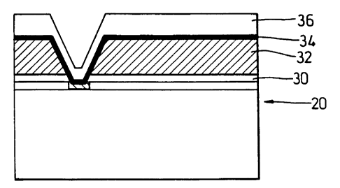
A substantially 14m thick layer of Silicon oxide 36 (SiOZ) (a support
material providing the support element) is deposited onto the surface of
the titanium 34, as shown in Figure 3h. This oxide layer 36 is patterned
and etched and it is ensured that the resists are removed using EKC.
In some embodiments of the process a matching layer (not shown) is
deposited or grown on top of the oxide layer.
The next step is to ash the wafer undergoing processing to remove the
sacrificial (polyimide) material. In the embodiment being described the
ashing process lasts for about 12 minutes. This ashing process releases
the support elements from the substrate and leaves a substantial void 38
between the titanium sensing material 34 and the passivation layer 30.
A final step of the process is to perform a rapid thermal anneal which
lasts for 30 seconds and is performed at 400 C.
The skilled person will appreciate that Figures 1, 2c, and 4 show the
structure of the micro-bridge device fabricated according to the process
shown in Figure 3.
Referring mainly to Figure 1 the micro-bridge device 48 is substantially
WO 01/14838 CA 02381311 2002-02-05 PCT/GBOO/03243
22
square in plan. The square portion comprises a support element 50 which
is suspended above a substrate (not shown) by legs 2, 4. The legs 2, 4
are separated from the support element 50 by slits 52, 54 which ensure
that the support element 50 has good thermal isolation from the substrate.
The structure of micro-bridge structure in Figure 1 is somewhat simplified
when considering the structure of the legs 2, 4. In Figure 1 each leg 2, 4
comprises a planar portion 56 in the same plane as the support element 50
but separated from it by the slits 52, 54. In addition to the planar
portion 56 there is provided an angular portion 58 which extends from the
planar portion 56 at an angle toward the substrate over which the support
element 50 is suspended. The planar portion of each leg 2, 4 is joined to
the support element 50 by a connecting region. The angular portion is at
a distal end from the connecting region.
The skilled person will appreciate that the specific structure of the
legs 2, 4 fabricated by the disclosed method may differ slightly. The
legs 2, 4 are formed by coating a depression etched into the sacrificial
material with a sensing material and coating the sensing material with a
support material.
On an under side of the support element 50 there is provided a metal
track 60 (this is shown as the metallic film in Figure 2c) which forms a
resistor having temperature dependent properties. The track 60 runs from
the substrate, up a first leg 2 of the micro-bridge device, across the
connecting region (forming a connecting region of the resistor) joining the
first leg 2 to the support element, meanders across the underside of the
support element 50, across the other connecting region (forming another
connecting region of the resistor) and down the other one of the legs 4.
WO 01/14838 CA 02381311 2002-02-05 PCT/GBOO/03243
23
As can be seen in Figures 4a and b in some embodiments the meanderings
of the track 60 have major portions running in directions substantially
perpendicular to one another. The meanderings ensure that the length of
the track 60 is maximised to increase the value of the resistance provided
by the track 60, which in this case is about 3kS2. The track is fabricated
from Titanium, having a temperature coefficient of resistance of about
0.35%/K.
Figure 4c shows an embodiment of the micro bridge structure with
meanderings with major portions running in substantially only one
direction.
The scanning electron micrographs shown in Figures 5 and 6 show the
track having a meandering nature with major portions running in
directions transverse to one another. It is believed that this meandering
nature helps to prevent radiation of a particular polarisation passing
through the micro-bridge.
The skilled person will appreciate that although the track is provided
underneath the support material its path is visible, in Figures 5 and 6, on
a top surface of the support material due to the nature of the processes
which are used to fabricate the micro-bridge structure.
The thickness of the SiO2 (the support material) from which the support
element is fabricated is made to be equivalent to one quarter of the
wavelength of the incident radiation of the wavelength of interest within
the SiO2. The skilled person will appreciate that the wavelength of the
radiation will be different in free space and within the SiO2. In this case
the SiO2 is made to be roughly l m thick.
WO 01/14838 CA 02381311 2002-02-05 PCT/GBOO/03243
24
In use, an array of devices as shown in the Figures is provided and
arranged to have radiation incident upon them. The support element 50 is
tuned to absorb radiation in the wavelength range 8 m-14 m (but may
alternatively be tuned to other wavelengths) and therefore experiences a
temperature change when such radiation is incident. This temperature
change causes the value of the resistance of the track 60 to change in a
known manner and this change of temperature can be used by the circuitry
to which the track 60 is connected to calculate the amount of radiation of
the wavelength of interest that was incident upon the support element 50.
Thus, the support element 50 is arranged to act both as a physical support
and as an absorber of radiation. The micro-bridge device has in its
simplest form two layers (a support material 36 and a sensing
material 34), which together provide three functions: physical support,
radiation adsorption and radiation detection.
The leg 2, 4 ensure that the support element 50 is mechanically supported
above the substrate but their design ensures sufficient thermal isolation so
that the thermal mass of the substrate does not affect the temperature
change of the support element.
Radiation of the wavelength of interest incident upon the micro-bridge
enters the bridge structure. Eventually this radiation hits the metallic
film 14 forming the track 60 which reflects the radiation back toward the
top surface of the micro-bridge. The pattern of the meandering track 60
is provided to ensure that radiation of all polarisations should be reflected
and therefore absorbed, thereby increasing radiation absorption. If the
meandering ran substantially in only a single direction it is possible that a
higher proportion of radiation being polarised in the specific orientation
may pass through the track than radiation of other polarisations (although
a large proportion may still be reflected). Having meanderings in more
CA 02381311 2002-02-05
WO 01/14838 PCT/GBOO/03243
than one-direction helps to reduce the amount of radiation that can pass
through the track.
Because the Si02 is 1/4 of the wavelength of the radiation of interest the
5 total optical path length from the top surface to the metallic film down to
the lower surface and then back to the top surface is 1/2 wavelength.
Therefore, destructive interference occurs in a region of the top surface
ensuring that a high degree of absorption of the radiation of interest
occurs.
In some embodiments a matching layer may be provided on a top surface
of the micro-bridge adapted to match the surface to free space i.e.
37752/square. The skilled person will appreciate that when a wavefront
passes between two mediums of differing refractive index a degree of
reflection will occur. The matching layer helps to minimise this
reflection and further increase the amount of radiation that is absorbed by
the micro-bridge. It is important to ensure that the amount of radiation
that is absorbed is maximised to ensure that the temperature change
experienced by the support element 50 is as large as possible.
The skilled person will appreciate that although this application largely
discusses absorption of radiation having a wavelength of 8 m-14 m the
technology described may have wider applications. Detecting wavelengths
of 8 m-14 m may be especially advantageous because it coincides with an
atmospheric absorption window wherein there is little absorption by the
atmosphere. The skilled person will further appreciate that there is a
further absorption window between 3 m-5 m which may also be used.
Further, it will be equally possible to fabricate devices which absorb
radiation outside these wavelengths. In such devices the materials and
structure of the bridge structure may simply need optimising for the
CA 02381311 2002-02-05
WO 01/14838 PCT/GBOO/03243
26
wavelengths in question.