Note: Descriptions are shown in the official language in which they were submitted.
CA 02381626 2002-02-08
WO 01/11478 PCT/LTS00/21617
ARCHITECTURE FOR AN INPUT AND OUTPUT DEVICE CAPABLE OF
HANDLING VARIOUS SIGNAL CHARACTERISTICS
to
FIELD OF THE INVENTION
The invention relates generally to architecture of an input and output device,
and
more particularly, to architecture of an input and output device capable of
handling
signal characteristics among different control system applications.
BACKGROUND OF THE INVENTION
Typically handling of input and output (I/O) is one of the most complex and
costly parts of a control system. As signal characteristics vary significantly
among
different applications, the handling of the signals becomes unique to the
application. For
2o example, in aerospace applications, the I/O design tends not to be portable
among
different aircraft, or even among the different control units on the same
aircraft. With
the need for a new I/O design for each control unit, the handling of I/O
becomes a major
cost factor.
Additionally, since such diverse designs do not allow reuse of I/O designs
across
multiple applications, additional costs are imposed in the purchase of many
types of
chipsets and components in the development and testing of new I/O designs.
Further,
costs are also imposed due to a need for interfacing hardware to interface the
new I/O
designs with various signals and data buses, as well as due to the volume and
weight of
I/O subsystems, since more power is needed to run the subsystems and more fuel
is
3o required to lift the subsystems of an aircraft.
Accordingly, there is a need for architecture for an I/O unit which interfaces
various signals and data buses so the same I/O unit design can fit different
applications
without requiring interfacing hardware.
CA 02381626 2002-02-08
WO 01/11478 PCT/US00/21617
Additionally, there is a need for architecture for an I/O unit which
integrates
multiple functions, such as processing a large number of signals, performing
signal
conditioning and filtering for a large range of signals, and conducting analog
and digital
conversion, to reduce volume and weight of the I/O subsystems and achieve
miniaturization.
to
SUMMARY OF THE INVENTION
The present invention provides a novel architecture for an I/O unit capable of
handling the I/O of analog and discrete signals in various applications, such
as control
systems for aircraft. The present I/O device can standardize the I/O hardware
for aircraft
and thus, significantly reduce the cost, weight and volume for the aircraft
system.
Miniaturization is achieved by integrating multiple functions and by using
state-of the
art chip technology to employ mixed signal design for the implementation of
the I/O
device. The I/O device is capable of processing a large number of signals,
performing
signal conditioning and filtering for a large range of signals, and conducting
analog and
2o digital conversion.
The I/O device includes programmable signal conditioning and signal control
circuitry for receiving signals, scaling the received signals to a
predetermined voltage
range, determining signal type for each of the received signals, and
controlling
input/output circuitry of the programmable signal conditioning and signal
control
circuitry for accessing input signals and generating output signals. The I/O
device
further includes conversion circuitry for receiving the input signals and
converting these
signals from analog to digital to enable the output signals to be digitally
processed, and
also receives digitally processed signals, converts the digitally processed
signals to
analog signals, and transmits the analog signals as output signals to the
programmable
3o signal conditioning and signal control circuitry. Bus interface logic
circuitry coupled to
the programmable signal conditioning and signal control circuitry for
interfacing the I/O
device with a bus for transfernng information to and from the I/O device is
also
included.
2
WO 01/11478 CA 02381626 2002-02-08 pCT~JS00/21617
High current and/or voltage conditioning circuitry for conditioning the
signals
within current and voltage ranges which are tolerable to microelectronics of
the
programmable signal conditioning and signal control circuitry may also be
provided, as
well as signal specific conditioning circuitry for conditioning the signals to
match the
electrical characteristics of the programmable signal conditioning and signal
control
1 o cmcmtry.
BRIEF DESCRIPTION OF THE DRAWINGS
Figure 1 is a block diagram of an I/O device according to the present
invention;
Figure 2 is a schematic illustration of a subassembly of the programmable
signal
conditioning and control circuit in accordance with one specific illustrative
embodiment
of our invention.
Figure 3 is a schematic illustration of the programmable amplifier of the
subassembly of Fig. 2;
Figure 4 is a block diagram of another illustrative embodiment of an I/O
device
2o according to the present invention; and
Figure 5 is a schematic illustration of a signal conditioning and conversion
chip
for the embodiment of Fig. 4.
DETAILED DESCRIPTION OF THE PREFERRED EMBODIMENTS
A. Conceptual Architecture
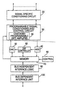
In Figure 1, there is illustrated a high-level functional block diagram of the
architecture for an I/O device according to the present invention. The I/O
device
includes the following blocks: High Current and/or Voltage Signals and Signal
Specific
Conditioning block 20; Programmable Signal Conditioning and Signal Control
block 30;
3o Analog-to-Digital Conversion (ADC) and Digital-to-Analog Conversion blocks
(DAC)
40 and 50; Digital Signal Processing (DSP) Controller block 60; Memory and
Control
blocks 70 and 80; Bus Independent Interface Logic block 90; and Bus Dependent
Interface Unit block 100.
3
WO 01/11478 CA 02381626 2002-02-08 PCT/US00/21617
Block 20 pre-conditions the large signals to within a tolerable range and
creates
the correct matching characteristic of the signal. It should be noted that if
the voltage
and current of the signal are within tolerance for a microelectronic chip,
such as a CMOS
chip, this block is not necessary and is not included. Block 20 includes the
following
sub-blocks, not shown: High Current and/or Voltage sub-block and Signal
Specific
1o Conditioning sub-block.
The High Current and/or Voltage sub-block scales any high voltage signal to
within a tolerable range. This sub-block converts the extreme signal
conditions to within
the signal range of the CMOS chip utilized in this specific illustrative
embodiment of the
present invention. The Signal Specific Conditioning sub-block matches any
signal with
a specific termination resistance. Also, any special circuit structure, such
as a wheat-
stone bridge, is constructed by this sub-block.
Block 30, as shown by Figure 1, receives all the high voltage signals that
have
been scaled to within a reasonable range. However, it also receives some small
signals
which are still not within the full range of the ADC 40 or DAC 50. Further,
there is no
control over the DAC 50 driving a potential input. Block 30 addresses both
issues and is
configurable to handle both discrete and analog signals. In addition, the
signal interface
can be configured for both input and output, i.e., bi-directional. Block 30
includes two
sub-blocks: Programmable Signal Conditioning sub-block including cascaded
programmable amplifiers and Signal Control sub-block, not shown.
The Programmable Signal Conditioning sub-block is programmable to handle
differential or single-ended signals and scales them to the full range of ADC
40 or DAC
50. The scaling step produces the maximum resolution for a number of signal
ranges
using a single range converter. The Signal Control sub-block enables or
disables the
output driver of a signal. If a signal has been programmed as input, then DAC
50 output
3o must be disabled or blocked. ADC 40 does not have to be disabled, even when
the
signal is programmed as output. Although it is never disabled, ADC 40 should
have the
programmability to select inputs other than the signal to which it is mapped
(e.g., a
calibration or a test signal).
4
WO 01/11478 CA 02381626 2002-02-08 pCT/[JS00/21617
ADC 40 and DAC 50 convert the analog signals into and out of the digital
realm,
respectively. These blocks can be implemented through a number of converters,
each
multiplexed to a subset of signals; or there can be one converter implemented
for each
signal. In any case, it is preferable to have an overall sampling or refresh
rate for each
signal.
1o DSP Controller block 60 is optional and can be pushed to whatever processor
or
controller is at the other end of the bus. Block 60 is where all digital
filtering and
manipulation take place as described in detail below. With a sufficient
overall refresh
rate, it can digitize an analog frequency component (LVDT or RVDT) and convert
it to a
meaningful value. Having block 60 enables manipulation of time critical
information
efficiently and reduces traffic over the system bus. It is herein assumed a
DSP
Controller is integrated within the I/O device of the present invention.
Blocks 70 and 80 handle the mapping of the internal registers of ADC 40, DAC
SO and Signal Conditioning and Control blocks 20 and 30 into an appropriate
memory
map. The mapping allows reconfiguration and access to I/O data registers.
Blocks 70
2o and 80 could be merged with either the Bus Independent Interface Logic
block 90 or the
DSP Controller block 60. Blocks 70 and 80 also serve as a placeholder for any
support
logic needed to keep the DSP Controller block 60 performing optimally, e.g., a
sequencer to upload the data from ADC 40 to memory 70. Memory block 70
advantageously comprises control circuitry and registers.
The Bus Independent Interface Logic block 90 outlines the protocol to be used
to
interface with the Bus Dependent Interface Unit block 100. Block 90 could be a
proprietary bus interface or a bridge to a daughter board interface (e.g., a
PCI bridge for
a PMC interface). Block 100 links the I/O device to a controller or management
computer. Block 100 translates between block 90 and whatever bus has been
selected.
3o It is contemplated that block 100 could be implemented as a permanent
fixture with
programmable logic for different protocols and interchangeable layers or as a
separate
entity to be "plugged into" the board, such as mezzanine or daughter boards
(e.g., a
PMC).
5
WO 01/11478 CA 02381626 2002-02-08 pCT~JS00/21617
B. Detailed Design of the I/O Device
1. High Current and/or Voltage Signals and Signal Specific Conditioning
The function of block 20 is to buffer or condition within a reasonable bound
the
high voltage or high current signals before they can be transferred to the
Programmable
Signal Conditioning and Signal Control block 30. It is also contemplated that
block 20 is
to equipped with specific circuit structures to enhance the signal or at least
the data that it
represents (such as, e.g., a wheatstone bridge), before the data is
transmitted to block 30.
A certain degree of customization is necessary for block 20.
2. Programmable Signal Conditioning and Signal Control
When the signals reach block 30, they are within a reasonable range, although
some signals are still quite small. Further, there is a mix of analog and
discrete signals,
single-ended and differential, and input and output signals that all need to
be sorted out
and dealt with accordingly. There is no predefined location for any such
class' of signals
within this block 30, although the implementation of this block 30 may impose
a minor
restriction on the placement of differential input signals. There is a maximum
flexibility
at this stage. Also, in passing these signals on to the next stage, this stage
filters out the
higher frequency noise and spikes. The approach calls for a high frequency
roll-off and
for lower frequencies to be filtered out digitally, if necessary.
a. Analog and Discrete Signals
It is important at this point to detail how the different analog and discrete
signals
are handled as a single-ended analog input. This is possible because the high
current
and/or voltage signals have been conditioned to "fit" within the range of the
analog
signals. Treating them differently would be redundant, use more area and thus
increase
cost. Handling the signals similarly has many benefits for the discrete
signal, such as
programmable hysteresis and programmable debounce. This will be explained more
3o fully in the DSP Controller section below.
b. Single-Ended and Differential Signals
Since discrete signals have been classified as single-ended analog signals,
there
are really only two classes of signals, the single-ended and the differential
signals. These
6
2 _06-2001 =-; : ~ ? 201?S365o4 HDIJc.YW=.1L LAW D~PT PAa~ ~5.~~.~.~ S~
CA 02381626 2002-02-08
s need to be lianandlcd so that the differential signal ke s its irate
ap grity and the s,~gle-ended
signal has a reference to iis. local ground. This section mainly deals with
input signals,
since, when used as an output, there is always a~ ground that can be
referenced" or, if, it is
a true differential signal, two single-ended signals can be paired together
with a commiort
ground for good signal integrity. ,
. The preferred design for the IIO, device : of the present invention includes
the
cascaded programmable di$'exential amplifiers ox receivers 35 between every
signal as
shown in Figure 2. As depicted in Fig. 2, the circuit 35 includes a plurality
of .
differential amplifcers I0$ to which the inputs are applied end output drivers
or . '
amplifiers I07 connected to the analog to digital snd digital to analog
circuits 40 and 50.
~s Each of the diffe~tial atnplifer'circuits 105, in accordanco'with an aspect
of our
invention, comprises, as shown in Fig. 3, $ differential amplifier 106, a
feedback path
' including a gain circuit 108 to which a gain control signal is applied, and
t",ra '
multiplexers 109 and 110 to which a calibration signal, is applic~i end M
whiah.the A and ' '
B inputs ere applied, as shown.
2o The programmability of the ataplifier 3~ will determine if the signal is
differential or single-ended. If the signal is differential, then the inputs A
and B are fed
directly into the di$erential amplifier 105. If the signal is single-ended,
then the signal is
muted to the positive side of the receiver lOS sad the negative Side is routed
to lvcaI
_.
ground. Tliis pragraommability is attained, in accordance with our invention,
by the
25 inclusion of the multipleaers '(MtJ~~109 and 110 and the gain circuit 108,
which are
controlled by the control antd calibration inputs.
The ability to route signals through the MIJXs 109 and 110 in any order yields
greater poiaver and flex~tbility. For instance, A and B could be reversed at
any time to
detect any DC~ offset that may be present in the amplifier. 'This also
relieves the
restriction o~ having an order to the positive and negative signals frnm~ a
differential
signal. "fhe only restriction left is that the signal9 must be "adjacent to
one arwther. Also,
in the case where an amplifier may be unused, the power and ground signets,
Fig. 3, may
be. routed with the appropriate gain in order to detect any brown, out or
spike in the
7 _.
Em a f a n qMENDED SHEET
WO 01/11478 CA 02381626 2002-02-08 pCT/[JS00/21617
power supply. The calibration signal also enables the system to be tested with
a known
voltage, or even a variable voltage, without disrupting the actual input
signal.
c. Signal Sizes
Signals have a known upper bound to them, which is the upper bound of the
capabilities of block 30. There are also signals that have an upper bound much
smaller
1o than the overall bound. Sampling these signals without amplifying them
first would
result in a loss of precision in the signal. This is also true when attempting
to output
small signals.
In order to compensate for this mismatch, there are programmable gains on the
input and output amplifiers 106. Options for preset gains are available to
input amplifier
105 to match the more popular signal ranges and scale them to the full range
of ADC 40.
Also, the inverses of these gains are available to the output drivers 107 to
emulate the
input and supply the excitation for such circuits, if needed. This allows
thorough bench
testing of the device by a digital loop-back, and opens up the ability of a
thorough Built-
In-Test (BIT) procedure.
2o d. Inuut and Output
The last variable to sort out is whether the signal is input or output.
Although
this is a fundamental and very critical characteristic of a signal, it is
easily programmable
in embodiments of our invention.
Putting an output driver 107 that has a tri-state function on each signal
(Figure 2)
achieves programmable input or output. As mentioned previously, the input
receivers or
amplifier 105 need not be disconnected, even if a signal is classified as
output. There is
no interference incurred and, actually, it serves as an excellent approach for
any loop-
back BIT that would be implemented. The only problem that can occur is if a
signal is
classified as input and the output driver 107 is active. This is solved by the
restriction
3o that the output driver 107 have "tri-state" or "High - Z" capability. This
way, if a signal
is classified as input, the driver 107 can be "turned off' and not interfere
with the input
measurement.
8
2~-Oo-20~ l
06/27/2001 17:17 20i393G~b4 HO!~1=YWc! L LAW D=PT PAG= US0021C~1
. CA 02381626 2002-02-08
S ,All configuration ox co~rol, information would come.. frora the Memory and -
Control functional blocks 70 and 80 and thus appropriately configure caeh
signs[ as
input or output and aI9o a 'tilizo tbic full rango of cithcr ADC 40 or DAC S0.
3. ADC sad DAC
ADC 40 and DAC 50 are critical parts of the IJO~device,' ., The granularity
must
i0 be very frne to acquire the precision outlined in the application
requircmGnts. All
coaver9ions mtust be fast in order to meet the timing goals and refresh rates
also
mandated by the perform goals. The implemcntetio~n could be handled a number
of
ways. Usually multiple signals are mi~tltiplctced~ptr each ADC or DAC. The
nn~mber of
ADC .(or DAC) depends on the number of input (output) signals and the
multiplexing
' 15 ratio.
4. DSP Contrntler .~ .
DSP Controller block ~0 digitally pmcesses the ~aals. Some examples of the
types of processing that can be performed are below.
s. Discrete Signals iouladon '
2o ' In the discrete realm, signals are either on or o~ However, discrete
signals need
to be shaped and filtorod, by DSP Controller block 60, which is able to do so
since the
discrete signals are treated as singlo-ended analog signals.
l, Slaw Rite
Instead of tuzning .a signal on 100°l0, signals can reach their
intarded value at a
25 ~ set rate. The signal can have a slew chaiaoter~stic to itr This is
realized by stePP~B ~
DAC 50 from an initial state, at ~rhatevcr.rate needed, to a destination state
and leaving it
there. This avoids ground bounce and overshoot.
ii,. ~1 Ya atipn
By characterizing a disaiete signal ss an analog entity, there is the ability
to set
30 . levels and thresholds. This is valuable when~specifying CMOS or TTL logic
levels for
input or output, and allows for hystercsis for signals by
not reporting them on or offuatil they have passed certain programmable
levels. -
9 ..
Emvf ,
AMENDED SHEET
CA 02381626 2002-02-08
WO 01/11478 PCT/US00/21617
iii. Pulse Width Modulation (PWM)
Pulse Width Modulation is also very flexible when using DSP 60. Signals can be
turned and modulated at almost any frequency or rate (depending on refresh and
inherent
slew rates). Power percentages are achieved easily using many different
methods and
frequencies. Also, the pulse can be slightly dewed, as described above, if
needed.
iv. Filtering (Debounce)
Programmable debouncing is also an option when using DSP 60. A discrete
signal may not be reported to a certain state until after the signal has
maintained a certain
value, using level detection, for a programmed amount of time. This feature is
also
limited to the number of samples per second that ADC 40 can function. If the
sampling
rate is high, then there is more precision available for debounce times.
b. Analog Signals Manipulation
The primary function of DSP 60 is to process analog signals, mainly to filter
them, as explained below.
i. Filtering
2o Almost every sort of real filter can be implemented. There are algorithms
for
High pass, Low pass, and Band pass filters. There are also Infinite Impulse
Response
(IIR) and Finite Impulse Response (FIR) filters. DC offsets can be calculated
and
eliminated or simply added. The Fast Fourier Transform can be applied to the
data
stream, if necessary. Filters are the largest and most obvious use for DSP 60.
ii. Phase and Freguency Information
Obtaining the frequency and/or the phase of a signal is relatively
straightforward;
there are many different algorithms and approaches. To calculate the frequency
of a
signal, the zero crossings need to be calculated with the sampling rate. By
counting the
number of samples between two positive-to-negative zero crossings and
accounting for
3o the sample time, the frequency is easily calculated. Averaging this value
within a time
window results in a very accurate frequency calculation. If a more precise
measurement
is needed, then linear interpolation can be used between the two points of the
zero cross
to find the exact crossing time.
CA 02381626 2002-02-08
WO 01/11478 PCT/LJS00/21617
Phase of one signal to a given reference can be calculated similarly. Given
(or
having calculated) a set frequency, the phase of another signal in comparison
can be
calculated by finding the difference of the zero crossings and calculating
that with the
period to find the phase. Again, more precise calculations can be implemented
by linear
interpolation of the zero crossing. It should be noted that both of these
techniques
to assume the signal's data stream has been properly filtered and that there
is only one zero
crossing and not multiple due to noise. That is why filtering is a crucial
function of the
DSP Controller block 60.
iii. Complex Calculations
DSP 60 processes the discrete and analog signals, and performs many more
functions autonomously without passing the information on to the processor at
the other
end of the Bus Dependent Interface Unit block 100. DSP 60 can implement a
frequency
to voltage converter or voltage to frequency converter. Algorithms exist for
LVDT or
RVDT excitation and position calculation that can be implemented on DSP 60.
Signals
can also be added, averaged, and voted (mid value theorem).
5. Memory and Control
The Memory and Control blocks 70 and 80 may advantageously be integrated
into DSP 60. Their main functions are to move data between ADC 40 and DAC 50,
DSP
60 and the Bus Independent Interface Logic block 90. This allows the user to
customize
the memory map and can create simple "input" and "output" memory locations for
DSP
60. These functions may be integrated into another block, such as DSP 60.
Blocks 70
and 80 also represent any additional memory needed for DSP 60 or any other
needed
glue logic.
6. Bus Independent Interface Logic
It is preferable that the functionality of the Bus Independent Interface Logic
3o block 90 is not integrated with another singular entity. There may be more
than one
Block 90 with separate protocols to support more than one selected bus, such
as VME
and PCI. Although this is an implementation issue, it should not be viewed as
a limiting
factor.
11
CA 02381626 2002-02-08
WO 01/11478 PCT/IJS00/21617
Block 90 can be an abstract layer; i.e., it can be implemented as a
programmable
device or in software. In this layer all data transfers are wrapped into one
singular
protocol to communicate with the Bus Dependent Interface Unit block 100. In
this way,
regardless of what system bus is being interfaced to, the information will be
transferred
to block 100 in the same format. Thus, this layer hides the bus-specific
interface details
from the other components so that they do not have to be modified as a result
of
changing the bus. Block 90 creates a bound around the functionality of the I/O
device 10
and provides a defined port to be bridged to a targeted bus.
7. Bus Dependent Interface Unit
The Bus Dependent Interface Unit block 100 is a controller that handles the
bus
communication protocol and may advantageously comprise programmable logic sub-
block and a physical interface sub-block. The programmable logic translates
the selected
bus's protocol to a known interface protocol for transfer of information to
and from block
90. Accordingly, the programmable I/O device of the present invention can be
further
used to host the bus controller logic.
Using a field programmable device, e.g. an FPGA, it is possible to reconfigure
the unit for other system buses. There are multiple programmable devices
available in
the market that have the capacity and flexibility to host the logic of most of
the common
system buses and to be configured to generate the control signals expected by
the bus-
specific physical interface. Examples of system buses surveyed include IEEE
1394,
ARINC 429, Fiber Channel and Mil-STD 1553B. The bus selection is usually
application-dependent, however the architecture can be configured for the bus-
of choice
by loading the bus logic on the programmable device.
C. Integration Possibilities
There are a few blocks that lend themselves to being merged with other
function
3o blocks. This section outlines an approach that includes two mergers. One
implies an
ASIC for signal conditioning and conversion and another simply accounts for
logical
control. Such integration is employed in the illustrative embodiment of our
invention
depicted in Fig. 4.
12
CA 02381626 2002-02-08
WO 01/11478 PCT/IJS00/21617
Comparing Figure 4 with Figure 1, block 30 has been integrated with the ADC
40 and DAC 50 along with some of the functionality of blocks 70 and 80. The
integration creates a new block, Signal Conditioning and Conversion 130 which
includes
an integrated conversion circuit or sub-block 135. In addition, the Bus
Independent
Interface Logic and the rest of the Memory Control have been merged with the
DSP into
to a new Digital Signal Process or Block (DSP) 160.
1. Signal Conditioning and Conversion
The integration done at this level is all on silicon. The approach puts the
programmable drivers and receivers with ADC 40 and DAC 50 and various control
logic
on one chip for the integrated conversion circuit 135 as shown in Figure 5.
This design
greatly reduces chip count, board space, and connectivity issues.
The chip provides a miniaturized and configurable approach for handling of
input
and output signals and combines both signal conditioning and conversion logic
in a
compact implementation. The chip is designed to handle multiple signals in any
combination of discrete and analog, input or output and single-ended and
differential
2o from a few millivolts to a significantly higher voltage (e.g. 10 volts). It
is empowered
with a programmable-gain operational amplifier to scale the signal to a
supported
internal range while maintaining signal integrity and accuracy.
Logic of ADC 140 and DAC 150 is included on the chip. The interface to the
chip from the board side is completely in digital format. Reading a set of
registers from
a register and control block 160 accesses samples of input signals and writing
to these
registers generates output signals. ADC 140 and DAC 150 support a 12-bit
precision at
a high sampling rate. The chip of Figure 5 can be provided with a full loop-
back test to
support board-level BIT for performing diagnostics and integrity checks. The
chip is
designed to perform, given the right packaging, within harsh environment.
2. Enhanced DSP Controller
DSP 160 in this embodiment now incorporates the Memory Control and the Bus
Independent Interface Logic functions. By merging these functions, there is no
need to
completely segment the functions to separate lines of code or separate
controller chips.
13
2?-06-2001
06/27/2001 17:17 2~13S3o5o4 f-fGN=Y'~' L _Ak' DEPT pAG= US00216'I
CA 02381626 2002-02-08
s It should be noted that, although the integration of the Signal Conditioning
and
Conversion was all done in silicon, the integration, of DSP, Memory Control
and the Bus
Independent Interface Logic functions is purely functional and tray still
require multiple
chips to fulfill. A separate pragrannmable logic dtvice, aad external or dual
port memory
may be rueded to perform these functions; although, these fuactions.may be
integrated
on the DSP chip itself.
14
Empf AMENDED SHEET A'