Note: Descriptions are shown in the official language in which they were submitted.
CA 02381675 2002-02-08
WO 01/11396 PCT/US00/21936
DIRECTION OF OPTICAL SIGNALS BY A MOVABLE
DIFFRACTIVE OPTICAL ELEMENT
CROSS-REFERENCE TO RELATED APPLICATIONS
This application is cross-referenced to commonly assigned Application
Serial No. , filed on even date herewith (Attorney Docket No. LUC 2-027),
the disclosure of which is herein incorporated by reference.
STATEMENT REGARDING FEDERALLY SPONSORED RESEARCH
Not applicable.
BACKGROUND OF THE INVENTION
Within a fiber optic network, information from a source, in the form of an
electrical signal, is converted to an optical signal that can then be
transmitted
along a fiber optic cable to the intended destination where it is converted
back to
an electrical signal. In the modem world of Internet access, facsimiles,
multiple
telephone lines, modems, and teleconferencing, an incredible burden is placed
on
telecommunications networks to meet the ever-increasing demand for information
transmission services. Unaware of the capacities that would be required of
fiber
optic cables, relatively narrow bandwidths were calculated using classical
engineering formulas, such as Poisson and Reeling. The increased service needs
imposed upon these cables have resulted in fiber exhaustion and a concomitant
need for layered bandwidth management. For information on telecommunications
networks, see generally:
(1) www.webproforum.com/lucent3
One option for meeting the increased demand for information transmission
is to lay additional optical fiber cable. This option can be expensive,
however, and
is generally only practicable where the increased demand is relatively small.
Another method for dealing with this problem is called time division
multiplexing
(TDM). This method increases the speed at which the data is transmitted, speed
being measure in bits per second (bps). The bit rate is increased by slicing
time
into smaller increments such that a greater number of bits can be transmitted
per
unit time (e.g., per second). A drawback to this approach is that the detector
temporal frequency response limits the number of bits that can be transmitted
per
unit time.
CA 02381675 2002-02-08
WO 01/11396 PCT/US00/21936
2
Because of the limitations associated with TDM, another technique was
devised for carrying increased data load over existing fibers called
wavelength
division multiplexing (WDM). 1NDM involves slicing up the laser diode
transmitter
output wavelengths into multiple increments, each increment being modulated
S separately to increase the number of bits that can be transmitted per
second.
When the number of slices increases past a certain point, the system is
referred
to as a DWDM (Dense Wave Division Multiplexing) system.
DWDM increases capacity by assigning incoming optical signals to specific
frequencies within a designated frequency band, multiplexing the resulting
signals, and transmitting the resulting multiplexed signal via a single fiber.
The
signals are thus transmitted as a group over a single fiber. Spacing between
the
increments also is decreased using TDM with DWDM so that a greater number of
bits are transmitted per second. The signals then are demultiplexed and routed
by
individual cables to their destination. The transmitted signals can travel
within the
fiber optic cable at different speeds and in different formats, and the amount
of
information that can be transmitted is limited only by the speed at which the
signals travel and the number of frequencies, or channels, available within
the
fi ber.
A number of technological advances have made DWDM possible. Once
such advance was the discovery that by using fused biconic tapered couplers,
more than one signal can be sent on the same fiber. The result of this
discovery
was an increase in the bandwidth for one fiber. Another important advance was
the use of optical amplifiers. By doping a small strand of fiber with a rare
earth
element, usually erbium, an optical signal can be amplified without converting
it
back to an electrical signal. Optical amplifiers now are available which
provide
more efficient and precise flat gain with significant total power output of
about 20
dBm.
Narrowband lasers have also contributed to the increased capacity of
telecommunications networks. These lasers provide a narrow, stable, and
coherent light source, each source providing an individual "channel."
Generally,
to 80 channels are available for a single fiber. Researchers are working on
creating new methods for increasing the number of channels available for each
fiber. Lucent Technology's Bell Laboratories has demonstrated a technique for
multiplexing, or combining, 300 channels within an 80 nm segment of the
spectrum
35 using a femtosecond laser. See:
CA 02381675 2002-02-08
WO 01/11396 PCT/US00/21936
3
(2) Brown, Chappell, "Optical Interconnects
Getting Supercharged," Electronic
En ineering Times, May 25, 1998; pp. 39-40.
Given the greater number of channels, and corresponding signals, which
can be carried on a single optical fiber, multiplexing and demultiplexing has
become increasingly important. Current methods for multiplexing and
demultiplexing include the use of thin film substrates or fiber Bragg
gratings. For
the first method, a thin film substrate is coated with a layer of dielectric
material.
Only signals of a given wavelength will pass through the resulting substrate.
All
other signals will be reflected. See, for example, U.S. Patent No. 5,457,573.
With
fiber Bragg gratings, the fiber optic cable is modified so that one wavelength
is
reflected back while all the others pass through. Bragg gratings are
particularly
used in add/drop multiplexers. With these types of systems, however, as the
number of transmitted signals increases, so does the number of required films
or
gratings for multiplexing and demulitplexing. See U.S. Patent No. 5,748,350
and
U.S. Patent No. 4,923,271. Therefore, more efficient, less expense methods for
multiplexing and demultiplexing transmitted signals continue to be sought.
BRIEF SUMMARY OF THE INVENTION
A method and apparatus particularly useful for telecommunications
applications, such as switching, multiplexing and demultiplexing, is
disclosed. The
method commences by directing a source of input optical signals) (10) onto a
movable diffractive optical element or MDOE. A rotatable diffractive optical
element (RDOE) provides the most efficient type of MDOE. Each of the optical
signals is associated with a particular wavelength. Next, one or more output
stations) are supplied. Finally, the RDOE (12) generates output optical
signals)
and distributes them among the output station(s). The corresponding system for
treating the optical signals from a source thereof includes a source carrying
one
or more input optical signals, each of the signals being associated with a
particular wavelength. Also included is a movable diffractive optical element
positioned to intercept the source optical signals for producing one or more
diffracted output optical signals. Finally, one or more output stations are
positioned to receive the one or more diffracted output optical signals from
the
MDOE. "Diffractive Optical Elements" for use in the present invention bear
diffraction gratings for achieving their optical diffraction properties.
BRIEF DESCRIPTION OF THE DRA1MNGS
CA 02381675 2002-02-08
WO 01/11396 PCT/US00/21936
4
For a fuller understanding of the nature and objects of the present
invention, reference should be made to the following detailed description
taken in
conjunction with the accompanying drawings, in which:
Fig. 1 is a schematic representation of an RDOE switching input optical
signals emitted by a laser diode assembly onto lenses that are associated with
optical fibers;
Fig. 2 is a schematic representation like that in Fig. 1, except that the
output
optical signals are being switched to different lens pairs;
Fig. 3 is a schematic representation of an RDOE multiplexing input optical
signals from an optical fiber to four different output optical fibers (the
number of
output optical fibers being illustrative rather than limitative of the present
invention);
Fig. 4 is a schematic representation of an RDOE demultiplexing four input
optical signals from four laser diode assemblies to two optical fibers (the
number
of input and output signals/optical fibers being illustrative rather than
limitative of
the present invention);
Fig. 5 is a schematic representation of an RDOE switching three input
optical signals to all possible combinations of three optical output fibers
(the
number of input/output optical fibers being illustrative rather than
limitative of the
present invention);
Fig. 6 is a top view of Fig. 5;
Fig. 7A is a top view illustrating the tilting magnetic embodiment of an
Fig. 7B is a side view of the RDOE of Fig. 7A which shows the connection
of a magnet and coil to a printed circuit board;
Fig. 8 is simplified cross-sectional view of a plate bearing four posts
whose ends carry diffractive gratings of different spacing for diffracting an
input
optical signal (the number of posts and diffractive gratings being
illustrative rather
than limitative of the present invention) and
Fig 9 is a simplified perspective view of a plate whose surface carries a
diffraction grating for diffracting an input signal into a plurality of output
wavelengths.
The drawings will be described in detail below.
DETAILED DESCRIPTION OF THE INVENTION
The present invention provides a simple and elegant method for distributing
optical signals which may be utilized in a variety of uses, such as
multiplexing,
CA 02381675 2002-02-08
WO 01/11396 PCT/US00/21936
demultiplexing, switching, or any other application where it is desirable to
separate, combine or direct optical signals. Use of a rotatable diffractive
optical
element (RDOE) eliminates the need for optical apparatus, such as mirrors,
filters,
and thin films, which optical apparatus add complexity and expense
proportionally
5 as the number of optical signals to be treated increases.
Referring to the drawings, Fig. 1 a schematic representation of an RDOE
switching input optical signals emitted by a laser diode assembly onto lens
that are
associated with optical fibers. A source is provided, as represented by
numeral
10, which source is composed of one or more input optical signals, each of
which
is associated with a particular wavelength (~,) or energy. In accordance with
the
convention in the field, the term "wavelength" is used in this Application to
mean
one or more wavelengths or a band of wavelengths. Also throughout this
application, an "s" in parenthesis following a given element is used to
indicate the
presence of at least one or more of that element. For example, the term
"optical
signal(s)" means one or more optical signals. Source 10 in Fig. 1 is provided
by a
laser diode assembly, however, any other device or combination of devices
capable of supplying modulated optical signals) may be used. Such a device or
devices, for example, may include optical cable or fiber. Source 10 is
directed
toward the surface of rotatable diffractive optical element (RDOE) 12. RDOE 12
diffracts the input optical signals) of source 10 at different angles
according to
the diffractive equation:
(a) ~, = d(sin i+sin 8)
where,
7~ = wavelength of diffractive light (microns)
d = grating spacing of one cycle (microns)
i = angle of incidence from plate normal (degrees)
8 = angle of diffraction from plate normal (degrees).
For a fixed d and a fixed 7~, rotation of the RDOE in effect varies t to allow
different wavelengths to be diffracted at different angles, 8, thereby
generating
output optical signals. Specific characteristics and embodiments of the RDOE
12
will be discussed in greater detail later.
Three output stations are provided, as at 14, 16 and 18, for receiving the
diffracted output optical signals, 7~1 and ~,2, as shown at 20 and 22,
respectively.
With RDOE 12 at a first position as depicted in Fig. 1., output stations 14
and 16
receive output optical signals 20 and 22. Fig. 2 depicts RDOE 12 rotated to a
CA 02381675 2002-02-08
WO 01/11396 PCT/US00/21936
6
second position, the rotation direction being in the plane parallel to RDOE
12. In
this second position, the angle at which the optical signals are diffracted
has
changed and output optical signals now are directed at output stations 16 and
18.
Thus, by rotating RDOE 12, optical signals) may be switched among a number of
output station(s). Output stations 14, 16, and 18 shown in Figs. 1 and 2 are
optical fibers, but the output stations) may be any mechanism capable of
detecting or transmitting an optical signal. A system for switching a source
among three output stations illustrates a simple use of the method of the
invention.
As will be illustrated later, the simplicity of the method facilitates
distribution of
source of optical signals among a multitude of output stations. A lens
assembly
for focusing the optical signals) is provided in conventional fashion, for
example,
as shown at 24, 26, and 28 in Figs. 1 and 2. Structure necessary to implement
such a lens assembly is not described herein as it is well-known to those
skilled in
the art.
Fig. 3 illustrates the method of the present invention in a multiplexing
application, the input optical signals) of source 10 being supplied by optical
fiber
30. Input optical signals, ~,1, 7~2, ~,3, and 7~4, being transmitted along
fiber 30, are
directed toward RDOE 12, which retains its earlier numeration. Output stations
32, 34, 36, and 38 are positioned to receive the generated output optical
signals,
~,1, ~,2, ~,3, and ~.4, respectively, which are shown at 40, 42, 44, and 46,
respectively. RDOE 12 is shown being rotated among three positions: 58, 60,
and
62. Output stations, or optical fibers, 32, 34, 36, and 38, are the same as
those
output stations) described with respect to Fig. 1, but similarly could be
connected
to any mechanism capable of detecting or transmitting an optical signal. A
lens
assembly again is present in the form of lenses 50, 52, 54, and 56 to focus
the
optical signals. Similarly, a lens assembly 48 focuses the optical signals)
emanating from fiber 30 onto RDOE 12. Structure necessary to implement such a
lens assembly is not described herein as it is well-known to those skilled in
the
art.
Table I, below, illustrates the distribution of input optical signals, ~,1,
~,2, 7~3,
and ~,4, to the four output stations, 32, 34, 36 and 38, depending on the
three
different rotational positions of RDOE 12 as shown in Fig. 3.
TABLEI
Position 1 ~ Position 2 ~ Position 3
ut Station 1 ~ -- ~ W1
CA 02381675 2002-02-08
WO 01/11396 PCT/US00/21936
7
Out ut Station W1
2
Out ut Station W2 W3 W4
3
Out ut Station W3 W4 __
4
When RDOE 12 is in its first position, 58, ~,1 is directed toward output
station 34;
signal ~,2 is directed toward output station 36; and signal 7~3 is directed
toward
output station 38. No output optical signal is received by output station 32.
With
the RDOE 12 in its second position, 60, in Fig. 3, optical signals 7~1, 7~2,
7~3, and 7~4
are directed to output stations 32, 34, 36, and 38, respectively. When RDOE 12
is
in position 3, as at 62, output station 32 receives signal 7~2, output station
34
receives signal 7~3, and output station 36 receives signal 7~4. No output
optical
signal is received by output station 38. Rotating RDOE 12 to other positions
permits other combinations of output optical signals to be distributed among
the
output stations. In this regard, it will be appreciated that the number of
output
optical signals) and number of output stations) depicted in the drawings is
merely illustrative as a greater or lesser number could be used in accordance
with the precepts of the present invention.
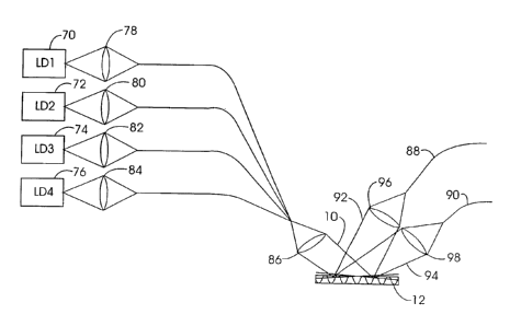
Fig. 4 shows yet another implementation of the present invention in a
traditional demultiplexing application. Source 10 is originates from the
combined
output of four laser diode assemblies, 70, 72, 74, and 76. A lens assembly, in
the
form of lenses 78, 80, 82, 84, and 86, directs source 10, provided by the
laser
diode outputs from laser diode assemblies 70, 72, 74, and 76, onto the surface
of
RDOE 12. Output stations 88 and 90 are provided to receive diffracted output
optical signals 92 and 94. In previous Figs. 1-3, the output stations each
received
a single output optical signal. As shown in Fig. 4, however, the output
stations
also may receive multiple output optical signals. A lens assembly, composed of
lenses 96 and 98, will determine what range of output optical signals will be
directed to output stations 88 and 90, respectively. Again, rotation of RDOE
12
directs diffracted output optical signals 92 and 94 between and onto lenses 96
and 98.
Fig. 5 shows a 3-dimensional view of the present invention in a switching
application, where all possible combinations of three input optical signals
are
directed onto three output lines, each combination corresponding to a
different
position of RDOE 12. Source 10 provides the three input optical signals,
7~1,~,2,
and ~,3. These optical signals are directed onto RDOE 12 that is located below
CA 02381675 2002-02-08
WO 01/11396 PCT/US00/21936
8
and parallel to source 10. Again, the number of source signals was chosen to
illustrate the present invention and not as a limitation of it.
Optical connectors positioned to receive the diffracted output optical
signals are spatially located along the surface of a hemisphere shown
generally
at 116. Output stations 110, 112, and 114 are located on lines of equal
latitude on
hemisphere 116. Four optical connectors are located along each latitude of
output
stations 110, 112, and 114. One wavelength is diffracted to all optical
connectors
located along each line of latitude. For example, output station 110, having
optical
connectors 130, 132, 134, and 136 will receive diffracted output optical
signal ~,1.
Output station 112, having optical connectors 138, 140, 142, and 144, will
receive
output optical signal ~.2. Output station 114, having optical connectors 146,
148,
150, and 152, will receive output optical signal ~,3. ~,3 will have a longer
wavelength than ~,2 which will have a longer wavelength than ~,1.
While the output stations have been described as being along equal lines
of latitude for efficiency, it will be appreciated by one skilled in the art
that the
output stations) may be located along non-parallel latitudes so long as the
optical
connectors located thereon are non-intersecting. Further, the spatial
positioning
of the output stations) have been described as being along the surface of a
hemisphere, however, this shape is intended to be illustrative and not
limiting of
the present invention. Positioning of the output stations) around the RDOE may
be in any desired configuration.
A conventional combiner (not shown) connects each output station's
optical connectors to an output fiber or cable. If there are n output fibers,
then
there must be n combiners, i.e., one for each output station. For the example
shown in Fig. 5, n = 3. For example, a combiner will combine optical
connectors
130, 132, 134, and 136 along output station 110 to a first optical fiber.
Another
will combine 138, 140, 142, and 144 to a second optical fiber. Finally, 146,
148,
150, and 152 will be combined and connected to a third optical fiber.
Looking to Fig. 6, a top view of the optical connectors illustrated in Fig. 5
is
shown. The components of Fig. 6 retain the numeration of Fig. 5. RDOE 12 is
rotatable to eight positions, shown at 154, 156, 158, 160, 162, 164, 166, and
168.
In each position, wavelengths will be diffracted to optical connectors located
along equal lines of longitude. (sphere 116, Fig. 5). Note that the RDOE 12
axis of
rotation is perpendicular to the grating plane. When RDOE 12 is positioned at
position 154, no output optical signals are conveyed to any optical
connectors. At
position 156, output optical signal ~,3 will be received at output station
114. Output
stations 110 and 112 will not receive signals.. With RDOE 12 in a third
position, as
CA 02381675 2002-02-08
WO 01/11396 PCT/US00/21936
9
shown at 158, output optical signal 7~1 will be received at output station 110
by
optical connector 134. No output optical signal will be received at output
stations
112 and 114. This grating will continue for all 8 positions.
Table II shows the optical signal combinations for each of the eight
positions to which RDOE 12 is rotatable.
TABLE II
Position Out ut StationOut ut StationOut ut Station
No. 1 2 3
1 0 0 0
2 0 0 1
3 0 1 0
4 1 0 0
5 1 0 1
6 0 1 1
1 1 0
8 1 1 1
When directing n input optical signals from source 10 to n output stations,
there
must be n~2" optical connectors, to permit all combinations of the n signals.
Each
of the n combiners will combine 2"'' optical connections. The resolution of
RDOE
12, i.e., the number of positions to which it may be rotated, must be
360°/2".
If the system depicted in Fig. 5 were being used in a multiplexing
application, combiners would be used to combine the output of the optical
connectors in each of the eight positions. For example, one combiner would
combine optical connectors 132, 144, and 150. The output to the optical fiber
would, thus, be optical signals of 7~1, 7~2, and ~,3. Another combiner would
be
positioned to combine optical connectors 130 and 138. This output, optical
signals
~,1 and 7~2, would be transmitted to a different optical fiber, and so on. In
a
multiplexing application, the number of combiners required would be 2".
The present invention, then, includes directing of output optical signals) to
one or more output stations by varying the effective spacing of a diffractive
optical element through rotation. One embodiment for RDOE 12 involves the use
of
a diffraction grating on a thin film that is connected to an energy source,
energizable for movement of the film. Such movement changes the effective
spacing of the diffraction grating on the film. A diffractive grating or
hologram may
be embossed on the thin film to form the diffractive grating. The film may be
PVDF
CA 02381675 2002-02-08
WO 01/11396 PCT/US00/21936
or any other piezoelectric film that deforms by a small amount when subjected
to
an electric field. The diffractive grating or hologram embossed on the thin
film is
rotated about a pivot point located at any position along the thin film. This
pivot
point may be, for example, at either end or at the center of gravity. The
energy
5 source, energizable to move the thin film, may be provided in any number of
electromagnetic configurations. One such configuration includes the
combination
of an energizable coil, or multiple coils, with the thin film, the combination
being
pivoted at the center. Magnets are located either below or to the sides of the
film
such that when the coils are energized, a magnetic flux is created and the
film
10 with its diffractive grating rotates about the pivot axis. Such structures
are
described in further detail in U.S. Patent No. 5,613,022, entitled
"Diffractive Display
and Method Utilizing Reflective or Transmissive Light Yielding Single Pixel
Full Color
Capability," issued March 18, 1997, which hereby is expressly incorporated
herein by reference.
Looking now to Fig. 7A, a top view of one embodiment of an RDOE, shown
generally at 12, is revealed to include the improved moving magnet embodiment.
A
holographic diffraction grating is provided at 182. Diffractive grating 182 is
attached to a magnetic component that is a permanent magnet (shown at 184 in
Fig. 7B). Diffractive grating 182 may be physically attached to magnet 184 or,
alternatively, diffractive grating 182 and magnet 184 each may be affixed to
an
additional element to form the attachment. Magnet 184 rests upon pivot 186
which
is made of ferromagnetic material and, therefore, attracts magnet 184 and
holds it
in place while still allowing the tilting motion to take place about pivot
186.
Connecting to, part of, or adjacent to, pivot 186 is current carrying
conductor 188
that is connected to FET (field effect transistor) 190. As such, magnet 184
and
coil 188 are magnetically coupled.
With current flowing through wire 188, a magnetic field is created which
exerts a force on magnet 184. Because magnet 184 is not in a permanently fixed
position, the force created by the current in wire 188 will cause magnet 184,
and
associated diffractive grating 182, to rotate about pivot 186. The direction
of
rotation of magnet 184, and associated diffractive grating, about pivot 186
depends on the direction of the magnetic field associated with magnet 184 and
the
direction of current flowing through wire 188. Reversing the polarity of the
current in wire 188 changes the direction of the force created, causing the
magnet to rotate in the opposite direction. Electromagnetic shielding 192 is
provided to prevent the interaction of fields generated by external sources.
This
shielding may be composed, for example, of SAE 1010 steel. As will be obvious
CA 02381675 2002-02-08
WO 01/11396 PCT/US00/21936
11
to one skilled in the art, alternative configurations can be envisioned to
electromagnetically couple magnet 184 and coil 188 for movement of the magnet.
Several illustrative configurations are described in greater detail later.
Stops 194 and 196 prevent the rotation of magnet 184 beyond desired
bounds. A portion of magnet 184 has been cut away to reveal the presence of
stop 194. Stop 194 may include a capacitance probe or sensor which senses the
presence of a capacitor (not shown), for example, composed of aluminized
Mylar~', which is located below magnet 184 and indicates the position of
magnet
184. Once the magnet has been driven to a desired position, it is held in
place by
the magnetic fields surrounding ferromagnetic pins 198 and 200. Because of the
presence of these pins, magnet 184 may be held in position with little or no
current
flowing in wire 188.
Turning now to Fig. 7B, a side view of the RDOE of Fig. 7A is shown
revealing the connection of the above-described elements to a printed circuit
board. Numeration from Fig. 1 is retained. Printed circuit board (PCB) 202 is
seen
to have ground plane 204 and + voltage bus 206. FET 190 is connected in series
with conductor 188, ground connector 208 and + voltage connector 210 (Fig. 1 )
being connected to ground plane 204 and + voltage bus 206, respectively.
Similarly, the capacitance sensor located on stop 194 is connected to ground
plane 204 at 211 and + voltage bus 206 at 212. The connection of elements to
PCB 280 is intended to be illustrative and not limiting of the present
invention, as it
will be obvious to those skilled in the art that other arrangements may be
provided.
In addition to RDOEs involving manipulated films or pivoted magnets or
coils, the present invention may be implemented using one of a number of
planar
rotational embodiments of RDOE 12. For each of these embodiments, an array of
facets may be achieved on the RDOE by providing a single diffraction grating
of
constant spacing or an array of diffraction gratingss each of which may have a
different spacing wherein each diffraction grating element of the array may be
disposed in juxtaposition or may be spaced apart, or by using a holographic
diffraction grating array wherein the array of facets are superimposed. With a
single diffraction grating, a facet is associated with each rotational
position of the
FRE, thus creating an array of facets to an observer. Where each facet of the
array is a separate diffraction grating, the facets may be non-uniformly or
uniformly placed along or across RDOE 12, however, the location of each facet
within the array is known, for example, each location can be stored in the
memory
of a microprocessor. With the location of each facet in the array know, the
RDOE
CA 02381675 2002-02-08
WO 01/11396 PCT/US00/21936
12
may be rotated such that input signals) illuminate select facet(s). Thus,
desired
output signals) are generated and directed to appropriate output station(s).
Fig. 8 depicts a first planar rotational embodiment of RDOE 12. Posts 222a
222d extend from the outer periphery of selectively movable plate 220. To
facilitate movement, plate 220 may be formed being substantially flat and
circular.
A facet, in the form of a diffractive grating having a particular or constant
grating
spacing, such as formed from a photoresist (holographic diffractive grating),
is
carried on the outer end of each post 222a-222d. Each facet diffracts
wavelengths at different angles. When optical source 228 is projected onto
plate
220 it strikes post 222d according to the position of plate 220 in Fig. 8 for
diffracting energy from source 228 according to the grating spacing carried on
the
end of post 222d. By suitable rotation of plate 220, post 222c, 222b, or 222a
could be positioned to intercept source 228 for diffracting different levels
of
energy, again according to their diffraction grating spacing. It will be
appreciated
that rotating plate 220 can take the place of RDOE 12 in Fig. 7, for example.
Movement of plate 220 can come from at least two different sources.
Plate 220 could be attached at its center 218 to the spindle of a stepper
motor (not
shown) that may conveniently be manufactured to have a 0.1 °
resolution, for
rotation of plate 220 about axis 218 to bring each of the posts, 222a-222d,
into
position to intercept source 228. A linear actuator also may be pivotally
attached
to plate 220 to cause its rotation about axis 218. Alternatively, plate 220
could
bear magnets that interact with energizable coils 224a-224d, again for
rotating
plate 220 about center 218. Alternately, plate 220 could bear the coils and
one or
more permanent magnets could replace the coils as depicted in Fig. 8.
Alternately,
electro-statics could be used to drive the rotation of plate 220. Of course,
combinations of these motive methods, as well as other motive methods, could
be
employed to rotate plate 220, as those skilled in the art will appreciate.
Looking to Fig. 9 another rotational embodiment of RDOE 12 is shown. A
plate similar to that shown in Fig. 8 is revealed generally at 230. Plate 230
has an
outer periphery 232 and a top surface 234. For this embodiment, an array of
facets is provided along top surface 234 rather than along periphery 232 as
previously shown. Instead of providing posts each of which bears a diffraction
grating with a unique spacing, the array of facets may be provided across the
surface of plate 230. In its simplest form, plate 230 may bear a single
diffraction
grating, 236, which has a constant grating spacing. As plate 230 is rotated, a
different signal will be diffracted to eye station 242, each rotational
position of
RDOE 12 representing a facet. The number of facets in the array, thus, will be
CA 02381675 2002-02-08
WO 01/11396 PCT/US00/21936
13
determined by the number (or plurality) of positions to which RDOE 12 may be
rotated. Alternatively, it may be advantageous to provide a plurality of
diffraction
gratings (having the same or different spacing) on the surface of plate 230 to
create an array facets of RDOE 12, wherein each diffraction grating element of
the array may be disposed in juxtaposition or may be spaced apart. Thus, as
plate 230 is rotated about its axis, for example as shown at 238, light from
optical
source 240 will be diffracted at different angles to eye station 242 depending
on
the position of the plate and the particular facet or grating spacing being
illuminated. Variation of the effective spacing of diffraction grating 236 is
most
readily achieved by use of a holographic diffraction grating as described
above.
By rotating plate 230 with grating 236, a single input signal may be
diffracted into a
plurality of output wavelengths, the number of output wavelengths being
commensurate with the number of variations in grating spacing along the plate.
The shape of plate 230 is shown in Fig. 9 as being circular, however, other
shapes may be preferred. Those skilled in the art will appreciate that the
shape of
the plate may be designed to maximize the number of areas of varying grating
spacing and resulting output signals. Rotation of plate 230 may be
accomplished
utilizing electrostatics, a linear actuator, or a stepper motor as described
previously in connection with Fig. 8.
Preferably, an array of facets may be provided across the surface of
plate 230 by using a holographic diffraction grating array wherein the array
of
facets are superimposed, each facet being angularly oriented or offset with
respect to each other. Thus, the holographic film is developed such that at a
given position of plate 230 with respect to the source, a particular output
signal is
generated and directed to a select output station. For example, if plate 230
is
rotated 2°, i.e. from an initial position of 0°, incident light
of wavelength ~.~ is
diffracted and the generated output signal directed to a first output station.
By
rotating plate 230 to another position, for example 9° from the initial
position, input
signal ~,, is diffracted and the generated output signal directed to a second
output
station. For each position of the RDOE, multiple facets may be illuminated
simultaneously by multiple input signals to direct multiple output signals to
multiple
output stations. Rotation of plate 230 may be effected as previously
described.
Utilizing any of these rotational approaches, the number of output signals
that may
be generated by RDOE 12 is limited by the number of positions to which the
RDOE
may be rotated.
While the foregoing description has been addressed to the use of an
RDOE, a movable diffractive optical element (MDOE) could be used for movement
CA 02381675 2002-02-08
WO 01/11396 PCT/US00/21936
14
of a diffraction grating in x-y-z coordinates. It will be appreciated,
however, that
for efficiency purposes an RDOE represents a preferred embodiment.
In this application all citations are expressly incorporated herein by
reference.