Note: Descriptions are shown in the official language in which they were submitted.
WO 01/11647 CA 02381701 2002-02-07 PCT/US00/22076
Field Emission Cathodes Comprised Of Electron Emitting Particles and
Insulating Particles
TECHNICAL FIELD
This invention relates generally to field emission display devices, and in
particular,
to methods of manufacturing cathodes for field emission devices.
BACKGROUND
Field emission displays (FEDs) are flat panel display devices that combine the
size
and portability advantages of liquid crystal displays (LCDs) with the
performance of
conventional cathode ray tubes (CRTs). FED devices typically include a field
emission
cathode positioned opposite a flat screen coated with phosphors. The phosphors
emit light
in response to bombardment by electrons from the cathode to produce an image.
The field
emission cathode emits electrons when subjected to an electric field of
sufficient strength.
The cathode typically includes thousands of microscopic emitter tips for each
pixel of the
screen. It is principally the emissive nature of the cathode that give FEDs
the thin, flat
screen features of an LCD with the viewing angle, brightness, and response
speed of a
CRT.
While FEDs are potentially very attractive devices, a limiting factor in the
widespread adoption of the technology is the difficulty of manufacturing the
devices,
particularly the difficulty in manufacturing the FED cathodes. Field emission
cathodes
have been known for some time. See, for example, Spindt et al. J. of Appl.
Phys. 47, 5248
(1976). The field emission cathodes described therein typically comprise sharp-
tip metal
electron emitters, such as molybdenum cones having a tip radius of the order
of a few tens
of nanometers. A method of manufacturing such cathodes with Mo cone emitters
on a
conductive substrate using semiconductor fabrication techniques is described,
of example,
in U.S. Patent No. 5,332,627 to Watanabe et al. Another example of the use of
semiconductor fabrication techniques, including patterning and etching, to
manufacture
emitter cone structures is provided in U. S. Patent No. 5,755,944 to Haven et
al.
The benefits of using carbon in the form of graphite or diamond as the
emitting
material in a field emission cathode have been recognized. A manufacturing
process that
includes in situ growth of diamond emitter bodies, by for example, chemical
vapor
deposition (CVD) or flame deposition, or alternatively deposition of pre-
existing diamond
1
WO O1/11647 CA 02381701 2002-02-07 PCT/US00/22076
grit or powder is described in U.S. Patent No.5,747,918 to Eom et al. Another
approach to
fabricating a carbon-based field emitter is given in U.S. Patent No. 5,608,283
to Twichell
et al. which avoids diamond CVD and uses fewer semiconductor processing steps
than
some of the approaches reported above.
Despite the variety of processes for producing field emission cathodes that
have
been developed, there remains a need for improved manufacturing techniques
that avoid
the complications of previous approaches described above. It would be
desirable for the
improved techniques for field emission cathodes to be scalable so that large
field emission
displays can be fabricated at reasonable cost without defects.
SUMMARY
Electrophoretic deposition provides an efficient process for manufacturing a
field
emission cathode. Particles of an electron emitting material are deposited by
electrophoretic deposition on a conducting layer overlying an insulating layer
to produce
the cathode. According to an aspect of the present invention, insulating
particles are
mixed with electron emitting particles in the deposited layer. Desired
properties of a field
emission cathode include requisite adhesion strength of the emitting particles
to the
conducting layer, sufficient emission when an electric field is applied to the
cathode, and
spatial and temporal stability of the field emission. According to another
aspect of the
present invention, by controlling the composition of the deposition bath and
by mixing
insulating particles with emitting particles, an electrophoretic deposition
process can be
used to efficiently produce field emission cathodes with the desired
characteristics.
Electron emitting materials that can be used for the emitting particles
include metals,
semiconductors, metal-semiconductor compounds, and forms of carbon. For
example,
graphite carbon, diamond, amorphous carbon, molybdenum, tin, and silicon, all
in powder
form, are advantageously used as emitting particles. Beneficial particle sizes
are between
about 0.05 gm and about 20 gm. Dispersed, rather than uniform, particle size
distributions
are preferred to improve packing.
The insulating particles are composed of a material that has a band gap that
is
greater than or equal to about 2 eV and is available in powder form.
Particular examples
of insulating materials used for the insulating particles include y-alumina,
other alumina
phases, silicon carbide, and oxides of titanium and zirconium. Best results
are achieved
for insulating particles between about a quarter and about a half the
characteristic size of
2
WO 01/11647 CA 02381701 2002-02-07 PCT/US00/22076
the emitting particles. The ratio of emitting particles to insulating
particles varies between
about 0.1% to about 99% emitting particles by weight, preferably between about
5% and
about 50% emitting particles, depending on the particular materials. For
graphite carbon
particles as emitting particles and y-alumina particles as insulating
particles, a mixture with
about 20 % graphite carbon particles by weight gives advantageous results.
In electrophoretic deposition, particles suspended in a deposition bath are
deposited
onto a conducting substrate under the influence of an electric field. The
composition of the
deposition bath plays a crucial role in the electrophoretic deposition
process. According to
an aspect of the invention, the deposition bath for the field emission cathode
includes an
alcohol, a charging salt, water, and a dispersant. The dominant component of
the
deposition bath is a reasonably hydrophilic alcohol such as a propanol,
butanol, or an
octanol. A charging salt such as Mg(N03)2, La(N03)2, or Y(N03)2, at a
concentration of
between about 10-5 to 10"I moles/liter is added to the alcohol. The metal
nitrates partially
dissociate in the alcohol and the positive dissociation product adsorbs onto
the emitting
particles and insulating particles charging them positively. The water content
has a
significant effect on the adhesion of particles to the conductive layer and to
each other.
The dissolved charging salt reacts with hydroxide ions from the reduction of
water to form
a hydroxide that serves as a binder. Water content of between about 1% and
about 30% by
volume is used to increase the adhesion of deposited particles. The deposition
bath also
includes a dispersant, for example, glycerin, at a concentration of from 1% to
20% by
volume of the deposition bath. Particularly advantageous results are obtained
for
deposition of graphite carbon particles in the size range between about 0.1
and 1.0 m
mixed with about 0.05 m y-alumina particles in a ratio of 20: 80 by weight in
a deposition
bath of isopropyl alcohol containing 10-3 molar Mg(N03)2 with 3% water by
volume and
1% glycerin by volume.
The field emission cathodes produced according to the method of the present
invention exhibit emission with excellent spatial and temporal stability. The
emitting layer
is a uniform deposit and has good adhesion to the underlying substrate. The
field emission
cathodes so produced can be used as an electron source in a field emission
display device.
3
WO 01/11647 CA 02381701 2002-02-07 PCT/US00/22076
BRIEF DESCRIPTION OF THE DRAWINGS
Fig. 1 a is a schematic cross section of a field emission cathode according to
an
aspect of the present invention. Fig 1 b illustrates emitting particles bound
to the
conducting material of a field emission cathode.
Fig. 2 is a schematic diagram of an electrophoretic deposition cell in which
aspects
of the present invention are performed.
Fig. 3 is a plot of ln(J/E2) vs. 1/E where J is the current density and E is
the applied
electric field for a cathode according to an aspect of the present invention.
The points
represent the measured values and the straight line is a least squares fit to
the data.
DETAILED DESCRIPTION
Electrophoretic deposition provides an efficient process for manufacturing a
field
emission cathode. Particles of an electron emitting material are deposited on
a conducting
layer by electrophoretic deposition to produce the cathode. In electrophoretic
deposition,
particles suspended in a non-aqueous medium are deposited onto a conducting
substrate
under the influence of an electric field. Desired properties of a field
emission cathode
include requisite adhesion strength of the emitting particles to the
conducting layer,
sufficient emission when an electric field is applied to the cathode, and
spatial and
temporal stability of the field emission. According to an aspect of the
present invention,
by controlling the composition of the deposition bath and by mixing insulating
particles
with emitting particles, an electrophoretic deposition process can be used to
efficiently
produce field emission cathodes with the desired characteristics.
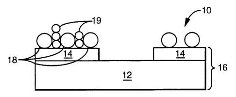
Fig. 1 is a schematic cross section of field emission cathode 10 which
includes
conductive material 14 supported on an insulating substrate 12. Substrate 12
and
conductive material 14 together constitute cathode support 16. Conductive
material 14 can
completely cover substrate 12 or it may form a pattern on substrate 12.
Particles 18 of an
electron emitting material are bonded to conductive material 14. Particles 18
are separated
from each other by insulating particles 19. The presence of insulating
particles 19
improves the properties of field emission cathode 10.
Without being bound to any theory, the beneficial effects of insulating
particles 19
are explained as follows. When field emission cathode 10 is placed opposite,
and spaced
from, an anode in vacuum, and a voltage is applied between cathode 10 and the
anode,
particles 18 of electron emitting material, eject electrons by field emission.
If multiple
4
CA 02381701 2002-02-07
WO 01/11647 PCTIUSOO/22076
particles 18 touch each other, they constitute a single emission site. In Fig.
lb, for
example, particles 18a, 18b, and 18c act as a single emission site. VWhen
insulating
particles 19 isolate the emitting particles from each other, each emitting
particle 18 can
potentially provide a separate emitting site. Increases in emission current
and in temporal
stability of emission are observed when insulating particles are used.
Substrate 12 of field emission cathode 10 is made of a rigid insulating
material
such as glass, ceramic, or plastic. Metals and metal oxides are used for
conductive
material 14. Particular examples of conductive materials used in conductive
material 14
include indium tin oxide (ITO), gold, chromium, aluminum, and chromium oxide.
Electron emitting materials that can be used in field emission devices include
metals,
semiconductors, metal-semiconductor compounds, and forms of carbon such as
graphite,
diamond, and amorphous carbon. For example, graphite carbon, molybdenum, tin,
and
silicon, all in powder form, are advantageously used as emitting particles 18
in cathode 10.
Additional emitter materials include tungsten, zirconium oxide coated
tungsten, n-type
doped silicon, porous silicon, metal silicides, nitrides such as gallium
nitride, and gallium
arsenide on a heavily doped n-type substrate. Beneficial particle sizes are
between about
0.05 m and about 20 m. Dispersed, rather than uniform, particle size
distributions are
preferred to improve packing.
As shown in Fig. 1 a, insulating particles 19 are smaller in size than
emitting
particles 18. Best results are achieved for insulating particles between about
a quarter and
about a half the characteristic size of the emitting particles. Insulating
particles 19 are
composed of a material that has a band gap greater than or equal to about 2
electron volts
and is available in powder form. Insulating particles that are approximately
spherical or
cubic in shape are used. Particular examples of insulating materials used for
particles 19
include y-alumina, other alumina phases such as a-, (3-, S-, and ~-alumina,
silicon carbide,
and oxides of titanium and zirconium. The ratio of emitting particles 18 to
insulating
particles 19 depends on the materials selected. The particle composition can
vary between
about 0.1% to about 99% emitting particles by weight, preferably between about
5% and
about 50% emitting particles. For example, for graphite carbon particles as
emitting
particles 18 and y-alumina particles as insulating particles 19, a mixture
with about 20 %
graphite carbon particles by weight gives advantageous results.
An electrophoretic deposition cell 20 used to produce field emission cathode
10 is
shown generically in Fig. 2. A negative electrode (cathode) 26 and a positive
electrode
5
CA 02381701 2002-02-07
WO 01/11647 PCTIUSOO/22076
(anode) 24 are suspended in a liquid deposition bath 22. Positively charged
particles 28
are suspended in the deposition bath. The method by which the particles are
charged is
discussed below. Voltage source 30 applies a voltage that produces an electric
field E in
the region between the positive electrode 14 and the negative electrode 12.
Under the
influence of electric field E, positively charged particles 28 migrate toward
the negatively
charged electrode 26. To produce field emission cathode 10, charged particles
28
comprise the desired mixture of emitting particles 18 and insulating particles
19. Cathode
support 16, of Fig. 1 is used as the negative electrode 26. Under the
influence of electric
field E, the mixture of particles 18 and 19 is deposited on cathode support 16
to produce
field emission cathode 10.
The composition of deposition bath 22 plays a crucial role in the
electrophoretic
deposition process. According to an aspect of the invention, deposition bath
22 includes
an alcohol, a charging salt, water, and a dispersant. The dominant component
of the
deposition bath 22 is a reasonably hydrophilic alcohol such as a propanol,
butanol, or an
octanol. Any alcohol that is miscible with water can be used. A charging salt,
such as
Mg(N03)2, is dissolved in the alcohol. One effect of the charging salt is to
impart an
electrical charge to the emitting particles 18 and insulating particles 19.
The Mg(NO3)2
dissociates partially in two steps in the alcohol:
Mg(N03)2 -~ Mg(NO3)+ + N03-
Mg(NO3)+ -~ Mg2+ + N03"
The Mg(NO3)+ ions adsorb onto the emitting particles 18 and insulating
particles
19, charging them positively. Charging salt concentrations between about 10"'
and
about 10'1 moles/liter are used.
The water content of the deposition bath 22 has a significant effect on the
adhesion
of the deposited emitting particles 18 and insulating particles 19 to the
conductive material
14 and of the particles to each other. When water is present as part of the
deposition bath,
the dissolved charging salt reacts to form a hydroxide that serves as a
binder. For
example, with Mg(N03)2 as the charging salt, the reactions:
2H20 + 2e" --> H2(g)T + 20H-
Mg(NO3)+ + 20H- -+ Mg(OH)2 + NO3-
lead to formation of magnesium hydroxide. Water content of the deposition bath
of
between about 1% and about 30% by volume has been found to increase adhesion
strength.
When water content is too high, evolution of hydrogen gas interferes with
particle
6
CA 02381701 2002-02-07
WO 01/11647 PCT/USOO/22076
deposition on conductive material 14. The charging salt is chosen, therefore,
such that the
salt of the metal is soluble in the chosen solvent (predominantly alcohol) but
the metal
hydroxide is insoluble in the chosen solvent. Other examples of charging salts
include the
nitrates of lanthanum and yttrium.
Finally, the deposition bath also includes a dispersant such as glycerin,
which also
is found to increase adhesion strength. Altemative dispersants include carboxy
methyl
cellulose, nitro cellulose, and arnmonium hydroxide. Including a dispersant in
the
deposition bath leads to a higher packing density of particles on the
patterned conductive
material 14. It has been suggested that the hydroxide binder deposits in
interstitial regions
between the particles and that adhesion is due to the contact points between
particles. By
increasing the packing density of the deposit, the number of contact points is
increased and
thus a higher adhesion strength is achieved. Dispersant concentrations can
range from
about I% to about 20 % by volume of the deposition bath. The optimal
percentages of the
different components of the deposition bath depend on the identity of the
emitting
particles, insulating particles, and of the individual components. As shown in
the
examples below, advantageous results were obtained for deposition of graphite
carbon
particles in the size range between about 0.1 and 1.0 m and about 0.05 m y-
alumina
particles in a ratio of 20: 80 by weight in a deposition bath of isopropyl
alcohol containing
10"3 molar Mg(N03)2 with 3% water by volume and 1% glycerin by volume.
The emitting particles and insulating particles are deposited on cathode
support 16
to produce field emission cathode 10 using a parallel plate method of
electrophoretic
deposition. In parallel plate deposition, a counter electrode, such as
positive electrode 24,
of the same size and shape as cathode support 16 is positioned parallel to and
spaced from
cathode support 16. For example, for an ITO patterned 5 cm square glass plate
as cathode
support 16, a stainless steel positive electrode 24 is placed at a spacing of
approximately 3
cm. The deposition bath as described above is prepared by combining the
alcohol,
charging salt, water, and dispersant. A mixture of emitting particles and
insulating
particles is added to the deposition bath. Suitable particle loadings are from
about 0.01 to
about 10 grams/liter with approximately 3-4 g/l being representative. The
particles may be
ball milled with glass beads to break up any agglomerates prior to being added
to the
deposition bath. For example, carbon particles in the size range of about 0.1
to 1.0 m are
ball milled with 3 mm glass beads for approximately 4 hours prior to
deposition.
7
CA 02381701 2002-02-07
WO 01/11647 PCT/US00/22076
The cathode support 16 and counter electrode 24 are placed in the particle-
loaded
deposition bath and a DC voltage is applied between conductive material 14 and
counter
electrode 24 to obtain a current density of from about 0.5 to about 2 mA/cm2.
The
thickness of the deposit is proportional to the amount of time the voltage is
applied. Time
and voltages may vary with deposition bath composition and cathode pattern.
For
example, a voltage of 200 V applied for 90 seconds gave a 25 m thick
carbon/alumina
deposit on conductive material 14 composed of a patterned layer of aluminum.
After the
voltage is turned off, the cathode is removed from the bath, rinsed with an
alcohol, for
example, the alcohol component of deposition bath 22, allowed to dry in air
and baked at a
temperature between about 400 and 550 C for from about 10 minutes to 2 hours
to convert
the hydroxide formed from the charging salt to an oxide.
The field emission cathode 10 produced by the electrophoretic method described
above appears uniform on visual inspection. Furthermore, the deposited layer
of particles
18 and 19 shows reasonable adhesion. The layer is not dislodged when a fmger
is wiped
across the surface in a procedure referred to as the "finger-wipe" test. As is
well known in
the art, achieving good adhesion of electrophoretically deposited layers has
been a
challenging technical problem in the past. Finally field emission cathode 10
exhibits
excellent emission characteristics.
The emission characteristics of field emission cathode 10 are measured in a
second
parallel plate configuration. In one example of a measurement configuration,
the cathode
10 is spaced about 150 m from a phosphor coated transparent conductor of
similar shape,
which constitutes a counter electrode, here the anode. The cathode 10 and the
anode are
connected to an appropriate power supply and placed in vacuum of approximately
10"5 to
10"6 torr. A positive potential ranging from about 200 to about 1500 V(1.3-
lOV/ m) is
applied to the anode and the emission current is recorded as a function of
applied voltage.
The emission current for field emission should follow the Fowler-Nordheim
equation:
ln (J/E2) = a(1 /E) + b
where J is the current density, E is the applied field and a and b are
constants. The plot of
ln (J/E2) vs 1/E in Fig. 3 for a field emission cathode 10 prepared according
to the
electrophoretic method described above and measured in the second parallel
plate
configuration exhibits the linear dependence characteristic of field emission.
The
phosphors on the anode allow identification of the field emission sites. Field
emission
cathode 10, according to the present invention, evidences sufficient density
of emitting
8
WO O1/11647 CA 02381701 2002-02-07 PCTIUSOO/22076
sites along the edges of conducting substrate 14 that the emission appears
continuous.
Finally, the emission of cathode 10, as measured in the second parallel plate
configuration
showed temporal stability. For example, as reported in Example 7 below,
cathode 10
exhibited less than a 5% deviation in emission current over an hour.
The field emission cathode can be combined with a driving anode and a phosphor
coated anode to produce a field emission display. The driving anode is
analogous to the
gate electrode of conventional field emission cathodes. Using an appropriate
pattern of the
cathode and gate electrode, desired display characteristics can be achieved.
Such a display
can easily be scaled to large sizes since the electrophoretic deposition
techniques and
equipment can be scaled accordingly to provide a uniform electric field on the
cathode
electrode during deposition of the emitting material. In contrast,
technologies dependent
on semiconductor processing techniques to fabricate the cathodes do not scale
easily.
The methods of electrophoretic deposition of field emission cathode 10 and the
characterization of the cathodes so produced are further illustrated in the
following
examples.
Example 1
Comparative Example
1.2 g of Hitachi GP-60S carbon graphite powder in the size range of 0.1-1.0 m
that had
been ball milled for 4 hours with 3mm glass beads were added to 300m1 of 10"3
M
Mg(N03)2 in isopropyl alcohol (IPA) to produce a deposition bath loaded at
4g/1. A 2.5 x
5 cm patterned aluminum substrate on a glass support was placed in the
deposition bath
positioned 3 cm from a stainless steel counter electrode. A DC voltage of 200
V was
applied for 90 seconds to produce a field emission cathode comprising a 25 m
deposit on
the substrate. The cathode was rinsed with IPA, dried in air and baked at 425
C for 20
minutes. Characteristics of the cathode produced in this and the following
examples are
listed in Example 8 below.
Example 2
Comparative Example
A loaded deposition bath was prepared as in Example 1 except for the addition
of 1%
glycerin by volume to the IPA. A 2.5 x 5 cm patterned aluminum substrate on a
glass
support was placed in the deposition bath positioned 3 cm from a stainless
steel counter
electrode. A DC voltage of 125 V was applied for 90 seconds to produce a field
emission
9
WO 0 1/11647 CA 02381701 2002-02-07 PCT/US00/22076
cathode comprising a 25 m deposit on the substrate. The cathode was rinsed
with IPA,
dried in air and baked at 450 C for 20 minutes.
Example 3
Comparative Example
A loaded deposition bath was prepared as in Example 1 except for the addition
of 3%
water by volume to the IPA. A 2.5 x 5 cm patterned aluminum substrate on a
glass support
was placed in the deposition bath positioned 3 cm from a stainless steel
counter electrode.
A DC voltage of 125 V was applied for 90 seconds to produce a field emission
cathode
comprising a 25 m deposit on the substrate. The cathode was rinsed with IPA,
dried in
air and baked at 450 C for 20 minutes.
Example 4
Comparative Example
A loaded deposition bath was prepared as in Example 1 except for the addition
of 1%
water and 1% glycerin by volume to the IPA. A 2.5 x 5 cm patterned aluminum
substrate
on a glass support was placed in the deposition bath positioned 3 cm from a
stainless steel
counter electrode. A DC voltage of 100 V was applied for 90 seconds to produce
a field
emission cathode comprising a 25 m deposit on the substrate. The cathode was
rinsed
with IPA, dried in air and baked at 450 C for 20 minutes.
Example 5
Carbon graphite particles as in Example I were combined with 0.05 m y-alumina
particles in a ratio of 1:9 carbon to alumina by weight and ball milled as in
Example 1. 1 g
of mixed particles was added to 300 ml of a deposition bath comprising IPA
containing 1
% water and 1% glycerin by volume to produce a deposition bath loaded at 3.33
g/l. A DC
voltage of 125 V was applied for 90 seconds to produce a field emission
cathode
comprising a 25 m deposit on the substrate. The cathode was rinsed with IPA,
dried in
air and baked at 450 C for 20 minutes.
Example 6
Carbon graphite particles as in Example 1 were combined with 0.05 m y-alumina
particles in a ratio of 1:9 carbon to alumina by weight and ball milled as in
Example 1. 1 g
WO O1/11647 CA 02381701 2002-02-07 PCT/US00/22076
of mixed particles was added to 300 ml of a deposition bath comprising IPA
containing 3
% water and 1% glycerin by volume to produce a deposition bath loaded at 3.33
g/1. A DC
voltage of 125 V was applied for 90 seconds to produce a field emission
cathode
comprising a 25 m deposit on the substrate. The cathode was rinsed with IPA,
dried in
air and baked at 450 C for 20 minutes.
Example 7
A deposition bath was prepared as in Example 6 except that carbon graphite and
y-alumina
particles were combined in a ratio of 2:8 carbon to alumina by weight. Field
emission was
observed from the cathode prepared from this bath at a field strength of <2V/
m. Current
deviation was less than 5% over an hour.
Example 8
The cathodes produced in Examples 1-7 were characterized according to the
uniformity of
the deposit on visual inspection, adhesion as determined by the finger-wipe
test and
uniformity of emission. Adhesion was considered average if deposited material
was not
removed down to the conductive substrate. Emission uniformity was judged poor
if fewer
than 10 separate emission sites per cm were observed along a conductive
substrate edge.
Observation of 20-40 sites/cm was considered average emission uniformity and
continuous
emission in which no individual sites could be observed was considered
exceptional
emission uniformity. Results are given in Table 1.
Table 1. Cathode Characteristics
Example Deposit Adhesion Emission
Uniformity Uniformity
Example 1 Good average poor
Comparative
Example 2 Good average poor
Comparative
Example 3 Poor average poor
Comparative
Example 4 Good average poor
11
WO 01/11647 CA 02381701 2002-02-07 PCTIUSOO/22076
Comparative
Example 5 Good average good
Example 6 Good better good
Example 7 good better exceptional
Thus it can be seen that the field emission cathode according to the present
invention exhibits emission with excellent spatial and temporal stability. The
emitting
layer is a uniform deposit and has good adhesion to the underlying substrate.
It can further
be seen that the method of electrophoretic deposition method according to the
present
invention provides an efficient process for manufacturing a field emission
cathode.
Although the invention has been described with reference to particular
examples of
field emission cathodes, the description is only an example of the invention's
application
and should not be taken as a limitation. Various adaptations and combinations
of features
of the examples disclosed are within the scope of the invention as defined by
the following
claims.
12