Note: Descriptions are shown in the official language in which they were submitted.
CA 02382082 2002-02-13
WO 01/13149 PCT/US00/20883
OPTOELECTRONIC DEVICE AND METHOD UTILIZING
NANOMETER-SCALE PARTICLES
CROSS-REFERENCE TO RELATED APPLICATION
This application claims priority from United States Provisional Patent
Application Serial
No. 60/148,993 filed August 13, 1999, entitled "Optoelectronic Propagation and
Switching
Below the Diffraction Limit."
STATEMENT REGARDING FEDERALLY SPONSORED RESEARCH OR
DEVELOPMENT
The U.S. Government has certain rights in this invention pursuant to Grant No.
DMR-9871850 awarded by the National Science Foundation.
BACKGROUND OF THE INVENTION
The present invention relates to the transmission and control of
electromagnetic energy
and, more particularly, to an optoelectronic device utilizing nanometer-scale
particles.
In recent years, designers of sophisticated, high speed electronic circuits
have become
interested in the use of optical signaling, both for its speed and because it
virtually eliminates
energy loss due to heat. Prior optical systems depend on the principle of
total internal reflection,
however, making them unsuitable for use when the lateral dimension of a
waveguide falls below
7J2n, which for visible light in glass is approximately 250 nanometers. In
many miniature
electronic circuits, such as modern high speed microprocessors, the size of
electrical conductive
paths is already less than half this limit. Also, there are limitations on how
sharply conventional
optical waveguides can be bent before their transmission properties are lost.
Continuous
conductive paths are also limited by their inherent electrical resistance when
they are made very
small. Thus, it is desirable to develop a form of interconnect which can be
made much smaller
than the diffraction limit and can be formed into arbitrary patterns without
sacrificing efficiency.
In a somewhat different field, nanometer-scale particles ("nanoparticles")
have been
fabricated and given a degree of order using a technique known as "self
assembly." By inducing
repulsive forces on close approach and longer range attractive forces on
particles in colloidal
suspensions, such particles are readily brought into closely packed arrays. An
example of this
is the colloidal synthesis and arrangement of silica-coated gold particles
described by L.M. Liz
Marzan, M. Giersig, and P. Mulvaney in Langmuir 12:4329 ( 1996). In this way,
control has been
obtained over the orientation of the particles and the spacings between them.
Metal colloids
useful for this purpose can be obtained from a number of commercial sources.
Linear chains of nanoparticles have been observed in suspensions of
polarizable particles
subjected to electric fields or magnetizable particles subjected to magnetic
fields. Fermigier and
Gast, J.Magn.Mater.122:46 (1992), confined paramagnetic particles in a narrow
channel and
examined the structures of the particulate agglomerates that resulted when
magnetic fields of
-1-
CA 02382082 2002-02-13
WO 01/13149 PCT/US00/20883
1 different strengths were applied. Induced dipoles caused the particles to be
attracted to one
another in the direction of the applied field and to repel one another in the
orthogonal direction.
The addition of surfactant molecules to prevent aggregation facilitated
reversible dipole-induced
ordering. Individual chains of such particles were not obtained, however, and
the arrays were not
suggested for use in the transfer of electromagnetic energy.
Thus, a need exists for structures capable of efficiently transfernng and
controlling
electromagnetic energy below the diffraction limit. The present invention
addresses these needs.
SUMMARY OF THE INVENTION
The present invention is directed to an optoelectronic device and related
method in which
nanoparticles are arranged in chains or "wires" for the transfer and control
of electromagnetic
energy in a variety of circuit configurations. The particles are spaced apart
along a preselected
path such that electrical polarization of one of the particles acts to induce
a corresponding
polarization in an adjacent one of the particles. These devices rely on near-
field interaction
between the nonoparticles to set up coupled polarization or plasmon modes.
Although the
coupling is believed to be primarily of dipoles created in the particles, in
some cases the coupling
can be part dipole and part higher order multiple.
The particles of a chain may include metals, semiconductors or other materials
capable
of being polarized, and polarization of a first particle may be created by
light. The particles
themselves may be individual atoms or molecules, or aggregations of atoms
and/or molecules,
and may be separated by dielectric particles or coated with dielectric
materials to create the
required spacing. In one embodiment, the particles are metallic and interact
with each other
through coupling of plasmon modes.
In a another embodiment, the optoelectronic device of the invention extends
from an input
device, which may be a light source, to an output at a terminal portion of a
chain. The output
device may be a detector of light or any other electromagnetic output of the
chain, or it may be
a waveguide or other suitable device. The spacing between particles may be
uniform or
nonuniform, and the chain may form arbitrary angles without affecting the
efficiency of energy
transmission.
The device may function as a switch, a filter or other suitable device,
depending on
configuration and use. Specifically, a first group of nanoparticles may extend
along a primary
path from a first end to a second end of the device, and a second group of
nanoparticles may
extend along a secondary path intersecting the primary path between the ends
of the primary path,
to modulate propagation of a polarization signal along the primary path.
Modulation occurs by
constructive or destructive interference between signals along the two paths,
and it is possible
to null the signal on the primary path by appropriate choice of the magnitude
and polarization of
the modulating signal.
-2-
CA 02382082 2002-02-13
WO 01/13149 PCT/US00/20883
I BRIEF DESCRIPTION OF THE DRAWINGS
The above and other features of the present invention may be more fully
understood from
the following detailed description, taken together with the accompanying
drawings, wherein
similar reference characters refer to similar elements throughout and in
which:
FIGURE 1 is a schematic representation of an optoelectronic device constructed
according
to one illustrative embodiment of the invention, in which a plurality of
nanoparticles are arranged
in a straight line;
FIGURE 2 is a schematic representation of an optoelectronic device constructed
according
to another illustrative embodiment of the invention, in which a plurality of
nanoparticles are
arranged in an angled configuration;
FIGURE 3 is a schematic representation of an optoelectronic device constructed
according
to a further illustrative embodiment of the invention, in which a plurality of
nanoparticles are
arranged in a configuration having a pair of separate output branches;
FIGURE 4 is a schematic representation of an optoelectronic device constructed
according
1 S to yet another illustrative embodiment of the invention, in which a
plurality of nanoparticles are
arranged in a configuration having a pair of input branches terminating in a
single output;
FIGURE 5 is a schematic representation of an optoelectronic device constructed
according
to a still further illustrative embodiment of the invention, in which a
plurality of nanoparticles
have different spacings between them;
FIGURE 6 is a somewhat diagrammatic representation of an optoelectronic device
constructed according to an illustrative embodiment of the invention, showing
the coupling of
a chain of nanoparticles with an optical waveguide;
FIGURE 7a is a diagrammatic representation of a chain of nonoparticles
constructed
according to an illustrative embodiment of the invention, showing the
application of a transverse
polarization of electrical charge to the nanoparticles;
FIGURE 7b is a diagrammatic representation of a chain of nonoparticles
constructed
according to an illustrative embodiment of the invention, showing the
application of a
longitudinal polarization of electrical charge to the nanoparticles;
FIGURE 8a is an idealized cross-sectional view of a chain of three
nanoparticles
constructed according to an illustrative embodiment of the invention, the
particles being
encapsulated by a dielectric material;
FIGURE 8b is an idealized cross-sectional view of a chain of three
nanoparticles
constructed according to another illustrative embodiment of the invention, the
particles being
separated by separate particles of a dielectric material;
FIGURE 9a is a diagrammatic representation of a plurality of disordered
nonoparticles
positioned on a faceted support structure in the absence of an applied field;
FIGURE 9b is a diagrammatic representation of the nonoparticles of FIGURE 9a
under
the influence of an applied field;
FIGURE 10 is a graph of the dispersion relation calculated for a linear chain
of equally
-3-
CA 02382082 2002-02-13
WO 01/13149 PCT/US00/20883
1 spaced metallic nanoparticles;
FIGURE 11 is a chart of the power transmission coefficients calculated for
arrangements
of nanoparticles of the invention under a variety of signal conditions; and
FIGURE 12 is a graph showing the proportion of electromagnetic energy
transmitted by
a chain of nanoparticles constructed according to the invention under
different conditions of
modulation by a separate applied signal.
DETAILED DESCRIPTION OF THE INVENTION
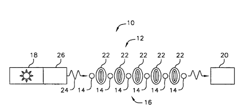
Referring to FIGURE 1, a novel optoelectronic device 10 according to one
embodiment
of the invention has a chain 12 of nanometer-scale particles 14 spaced apart
along a path 16 from
an input device 18 to an output device 20 for the transfer of electromagnetic
energy along the
path. The particles 14 are capable of being polarized by electromagnetic
energy, preferably in
the form of light, from the input device 18, to propagate a polarization
signal from one particle
to the next.
The device 10 relies on near-field interaction between the particles 14 to set
up coupled
polarization or plasmon modes to transfer energy along the path 16. These
interactions are
illustrated schematically by a set of field lines 22. FIGURES 7a and 7b show
possible
configurations of the field lines in greater detail. Considering the case in
which the initiating
signal is light, FIGURE 7a illustrates a beam of light 24 impinging on a first
particle 14 from a
lateral direction, creating a longitudinal polarization (L) in which electric
charge within the
particles is displaced substantially in the direction of the chain 12. This
occurs due to the
transverse orientation of the electric field vector (E) relative to the
direction of the light. As
shown in FIGURE 7a, in this configuration the electric field lines 22 between
adjacent particles
are fairly compact. FIGURE 7b illustrates the somewhat different case of light
impinging on the
first particle in a longitudinal direction, creating a transverse (T)
polarization and a less compact
arrangement of the electric field lines 22. As will be discussed more
rigorously below, the
longitudinal (L) and transverse (T) coupling configurations also result in
different speeds of
energy transport.
The particles 14 may be any of a variety of types as long as they are
considerably smaller
than the diffraction limit (7J2n, where ~, is the wavelength of the
transported energy and n is the
refractive index of the medium through which the energy is transmitted) and
can be suitably
polarized. In any such case, conductive portions of the particles are
separated from one another
to form a discontinuous path of conductive material which nevertheless serves
quite effectively
to transmit energy from one point to the other. Thus, the particles, as a
group, serve the basic
function of a continuous path for information transport and therefore may be
considered as a
"plasmonic wire." In one significant embodiment, the particles are metal
particles between
approximately 2 nanometers and eighty nanometers in radius. Metals are useful
because they
have a large number of free electrons which can be displaced to produce
distinct plasmon modes,
and because they absorb light strongly. Metal nanoparticles, in particular Au,
Cu and Ag,
-4-
CA 02382082 2002-02-13
WO 01/13149 PCT/US00/20883
1 strongly absorb light in the ultraviolet to near-infrared portion of the
spectrum and convert the
energy efficiently into collective electron motion. The exact frequency of
strongest absorption
depends on the metal, the particle shape and the host material. Semiconductor
materials and the
rare earth elements are useful for these purposes, as well. Alternatively, the
particles 14 may be
individual atoms or molecules, either organic or inorganic. In one specific
embodiment, the
particles are Ag particles approximately 25 nanometers in radius, with a
center-to-center spacing
of 75 nanometers.
Referring in greater detail to FIGURE 1, the input device 18 may be a light
source (either
coherent or incoherent) coupled to the first of the particles 14 by an optical
waveguide 26, and
the output device 20 may be an optical detector. Due to the diffraction limit
described above,
however, there is an intrinsic size mismatch between the waveguide 26
(typically 2250
nanometers) and the first of the nanoparticles 14 (typically ~ 50 nanometers).
This is dealt with
by operating at the surface plasmon resonance frequency, at which the
absorption cross section
of the metal particles can easily be increased by more than an order of
magnitude. An input
coupler operating at the surface plasmon frequency is shown schematically in
Figure 6, where
the flow of electromagnetic energy from the waveguide 26 to a first metal
nanoparticle 14 is
indicated by field lines 28. The effect of resonant enhancement of the
particle's absorption cross
section is shown by the bending of these lines toward the particle. Thus, the
light of the
waveguide is effectively focused into the first particle of the chain.
Considering the physics of
the nanoparticle chain in greater detail, it is well established that at the
surface plasmon frequency
light strongly interacts with metal particles and excites a collective
electron motion, or plasmon.
These frequencies are typically in the visible and near infrared part of the
spectrum. In
nanometer size particles (much smaller than the wavelength of the exciting
light, 7~), plasmon
excitations produce an oscillating dipole field. The dipole field produced by
one particle can
efficiently be coupled into another particle if in close proximity to the
first (distance « 7~). In
fact, it can be shown that coherent energy transport occurs along a chain of
equally-spaced metal
nanoparticles due to the near-field electrodynamic interaction between the
metal particles. This
results in the existence of coupled dipole or plasmon waves. This type of
coupling is analogous
to the process of resonant energy transfer, which is observed in systems that
contain closely-
spaced optically-excited atoms, molecules, or semiconductor nanocrystals. For
this reason
plasmonic devices can be made out of these entities, as well.
The transport of waves is often characterized by a so-called dispersion
relation. Using the
dispersion relation, one can determine, among other things, the following:
1) the frequencies and polarization directions of the plasmon waves that can
be
transported along a plasmon wire structures;
2) the velocity at which information can the transported through plasmonic
structures;
and
3) the frequency and polarization dependence of the transmission efficiency
around
corners.
-5-
CA 02382082 2002-02-13
WO 01/13149 PCT/US00/20883
1 In order to better understand the transport occurring in plasmon wire
structures, consider
a linear chain of equally-spaced metal particles separated by a distance d,
where each particle
is uniquely identified by an index m, as shown in the inset of FIGURE 10. If a
plasmon wave
were to propagate along this array, each particle in the chain would have a
certain dipole or
other polarization moment p;,m(t), where i denotes the polarization direction
of the plasmon
wave. Transverse (T) plasmon modes have polarization moments oriented
perpendicular to the
chain axis and longitudinal (L) plasmon modes have dipole moments along the
propagation
direction, where a mode is defined by the magnitude of the induced dipole
moments at each
particle. The transport characteristics are determined by the strength of the
electromagnetic
coupling between the particles. Due to this coupling, the electron motion in
one particle is
affected by the electron motion in its neighbors. In other words, the
polarization moments of
all particles in the chain are coupled. One can show this effect
mathematically in the equation
of motion for a dipole at an arbitrary location, m, in the chain. If only
nearest neighbor
interactions are considered, the equation of motion is given by:
pl,m \t/ ~Opi.m \t/ Yt~1 [pi,m-1 \t/+pm+1 ~t~~
The first term of equation (1) describes the dipole eigen-motion (oscillatory
motion
without interaction with its neighbors) at an angular resonance frequency wo.
The second term
incorporates electrodynamic interaction with the nearest neighbor dipoles at m-
1 and m+1. This
term is responsible for the existence of propagation wave solutions. The
coupling strength is
determined by the magnitude of 'y; and w,2, where y; is a polarization
dependent constant for
which yT = 1 and yL = -2. This shows that the coupling between dipoles for
longitudinal modes
is twice as strong as the coupling for transverse modes. For near-field
coupling, it can be shown
that w,2 = pVe/4~cm*EOnZd3, where p is the charge density in the particle, V
is the volume of the
particle, a the electron charge, m* the optical effective electron mass, so is
the free space
permittivity, and n is the refractive index of the host material. This
indicates that the strength
of the coupling is reduced when the distance between the particles is
increased, the refractive
index n of the host is increased, or the volume of the particle is reduced. As
an example, for an
array of 25 nm radius Ag particles spaced by 75 nm in vacuum (n=1), w, = 1.4 x
1015 rad/s'.
For this calculation we have used p = 5.85 x 1 OZZ/cm3 and m* = 8.7 x 10⁻³'
kg, which are values
for Ag. It should be noted that this equation of motion is derived assuming
nearest neighbor
dipole-dipole interaction and does not include damping effects. It is
straightforward to include
interactions between more distant neighbors, higher order interactions (e.g.
quadrapole), and
damping effects.
-6-
CA 02382082 2002-02-13
WO 01/13149 PCT/US00/20883
1 The equation of motion has propagating wave solutions that look like:
pa.m (t~ = P exp i(~t t kmd
S where P; is the maximum value of the dipole moment in the direction i, and k
is the wave vector
(k = 2~rJa,) of the plasmon wave. The dispersion relation is found by
substitution of equation 2
into equation 1:
~ 2 - ~o + 2y;a~; cos(kd~
This relation is plotted in FIGURE 10 for both the T and L modes. Also plotted
are dispersion
curves calculated including next nearest neighbor interactions (dashed
curves), and up to 5'"
nearest neighbor interactions (dotted curves). It is clear that nearest
neighbor interactions are
most significant for the transport properties of the nanoparticle chains. As
can be seen in the
figure, the dispersion relation relates the excitation frequency of the
plasmon wave to its k
vector (or 7~) for all of the allowed plasmon modes. For example, excitation
of a plasmon wire
at coo results in a k vector of ~/2d (or ~, = 4d) for both the longitudinal
and transverse waves.
Furthermore, it can be seen that plasmon modes exist only in a certain
frequency band around
coo, the bandwidth Ow of the plasmon modes. The group velocity vg,; (the
velocity of
information transport) can be calculated from the slope of the dispersion
relation. Very
generally, for any type of wave it holds that vg,; = dco/dk =
(dwz/dk)/(dco2/dco) = Y;co~Zd sin(kd)/w.
Since dcoz/dk is the slope of the dispersion curves in FIGURE 10, it can
easily be seen that at
a given co the L-waves propagate faster than the T-waves. At resonance, the
group velocities
for both the L-wave and the T-wave are maximum and Vg,L = 2vg,r. This results
from the
stronger EM coupling for L-waves than for T-waves. For an array of 25 nm
radius Ag particles
spaced by 75 nm in vacuum (n=1 ), we find that the group velocities at
resonance are vg,T = 2.9
x 10' m/s and vg,L = 5.8 x 10' m/s. These values are about two orders of
magnitude higher than
the saturation velocities of electrons in semiconductors. For these
parameters, the
corresponding bandwidths are OcoT = 7.9 x 10'4 s' (520 meV) and OcoL = 1.6 x
10'5 s' (1.05
eV).
Although the parameters of the optoelectronic device 10 can vary significantly
depending
on circumstances, the following parameters are preferred for certain
particular embodiments of
the invention:
Preferred More PreferredMost Preferred
Radius (r) of Metal 2~ _ ~ 10 - 40nm 25nm
Nanoparticle n
s ~ 4
Spacing (d) of
Snm - ~ 20 - 80nm 75nm
Nanoparticles n
_7_
CA 02382082 2002-02-13
WO 01/13149 PCT/US00/20883
1 Preferred More PreferredMost Preferred
Length (L) of chain ~ ~m 1 - S~m 2~m
.1 ~m -
a
Optical Index (nhS~ 1 - 4 1.2 - 3 1.5
Damping (K,,S~ a <lyi'
850nm; 1.3~m;
Wavelength (~,) 250nm - 2.S~m 300nm - 1.6~m
1.5 pm
Optical Cross Section1 - 10~ - ~ 5~
(aP~
5.86 X 1 OZZCm
3
Electron Density 10'g - I O24cm..1023cm 3 (Ag)
(ne) 3
cp (Radians) 0'~ -
Ag; Au; Na;
Cu;
Al; GaN; A1203;Ag; Au; Si02;
Polarizable MaterialsSiOz; ZnO; A1z03 or
for
Nanoparticles
polymer (e.g. combinations
polyamide)
Refernng now to FIGURE 2, an optoelectronic device 210 constructed according
to an
alternative embodiment of the invention extends between a light source 18 and
an output device
20 of the type described above in connection with FIGURE 1. The device 210 has
a chain 212
of nanoparticles 14 defining a first path segment 216 and a second path
segment 217 connected
end-to-end to form an angle cp therebetween. For purposes of generality, the
second path
segment 217 is also shown in FIGURE 2 as potentially being curved to a radius
r. In this case
the polarization of the particles 14 is transmitted in series along the first
path segment 216 and
the second path segment 217, resulting in an output signal 230 at a detector
or other output
device 20. The polarization traverses the transition point 232 between the two
path segments,
~d traverses the curved length of the second path segment 217, without a
significant loss of
intensity. Only the orientation of the polarization relative to the direction
of the path changes,
as shown by the change in orientation of the field interaction symbols 22.
An optoelectronic device 310 of FIGURE 3 is a form of signal splitter. It has
a primary
path 316 of nanoparticles extending between an input device 18 and a primary
output device
20 of the type illustrated in FIGURE1, but also has a secondary path 317
branching out from
the primary path at a location 332 at an angle of approximately ninety degrees
(90°). The
secondary path 317 itself contains another ninety degree (90 ° ) turn
before it reaches a secondary
output device 320. As demonstrated mathematically below, the polarization
signal imposed by
the light source 18 couples efficiently through the branch 332 and the turn in
the secondary path
_g_
CA 02382082 2002-02-13
WO 01/13149 PCT/US00/20883
1 317, with the only significant effect of these features being the amount and
polarization of the
light reaching the two output devices. Thus, the device 310, in its
generalized form, functions
as a signal splitter or a filter of the applied optical signal according to
the coupling principles
set forth below.
FIGURE 4 depicts an optoelectronic device 410 which is a modulator or switch
of the
nanoparticle type. The device 410 has a primary path 416 of polarizable
closely-spaced
nanoparticles 14 extending between a first light source 18 and a terminal
device 20, with a
secondary path emanating from a second light source 418, extending through a
ninety degree
(90°) turn, and joining the primary path at an intersection point 432.
As demonstrated
mathematically below, the interaction of the signals from the two light
sources (18 and 418)
depends on their relative frequencies, phases and polarizations, enabling the
signal from the first
light source 18 along the primary ,path 416 to be modulated, and even nulled,
as desired. For
complete destructive interference to occur, the wave sent out by the input
devices 18 and 418
should be out of phase and have the same polarization direction at the point
of intersection.
Considering again the theory of the plasmonic devices of the invention, the
transport of
electromagnetic energy through corners and tee junctions, as implemented in
the embodiments
of FIGURES 2, 3 and 4, can be calculated by requiring continuity of the
plasmon waves and
conservation of energy flux at the intersection of the chains. In general,
part of the incident
wave flows through the structure and part is reflected. The efficiency of the
power transmission
depends on the geometry of the structure, and the frequency and polarization
directions of the
plasmon waves that enter and exit a structure. As an example, we consider some
structures that
consist of chains and right angle corners. This greatly simplifies the
modeling since in that case
only three situations need to be distinguished: 1 ) in a turn an L-wave
transforms into a T-wave,
2) in a turn a T-wave transforms into an L-wave, and 3) in a turn a T-wave
remains a T-wave.
At certain values of w, the importance of the frequency and polarization
direction is manifested
in the dispersion relation showing only L-modes can exist and T-modes are
forbidden. This
implies that a right angle corner in which L-waves are transformed into T-
waves acts as a
frequency or polarization filter. It can also be shown that the transmission
efficiency through
any structure is maximum at w = cap, and in this discussion the value of wo is
assumed. Figure
2 shows calculated power transmission coefficients, r1, in the nearest
neighbor approximation
for all realizable right angle corner and tee structures. A r)-value of 1
corresponds to 100
transmission. Notice that all structures have r)-values exceeding 0.64,
showing that power flow
around right angle corners with dimensions much smaller than the wavelength of
light is
possible at high efficiencies. This is impossible in conventional dielectric
waveguide
3 5 technology, and is more akin to certain photonic crystal structures.
Beyond the nearest neighbor
dipole-dipole interaction approximation, more detailed analysis of plasmon
wire structures can
be made through full field electromagnetic simulations using, e.g., finite
difference time domain
calculations. It should be noted that the examples given above discuss
structures for which the
interparticle spacing is the same throughout the structure. This is definitely
not a necessary
-9-
CA 02382082 2002-02-13
WO 01/13149 PCT/US00/20883
1 requirement. In fact, structures may consist of various segments having
different interparticle-
spacing or other structures may have a non-periodic particle spacing, as
illustrated in FIGURE
5. With reference to FIGURE 5, polarizable nanoparticles 14 can be given
different spacings,
if desired. Thus, a path 516 of polarizable nanoparticles can be formed of a
first path segment
517 and a second path segment 519 to couple an input device 18 to an output
device 20. In this
embodiment, the path segment 517 has a center-to-center particle spacing of
d,, while the path
segment 519 has a particle spacing of d2.
The interference between the various signals of the modulation device 410 of
FIGURE
4 is illustrated graphically in FIGURE 12. These signals are the modulating
signal (M) of the
light source 418, the primary signal (S) of the light source 18, and the
transmitted signal (T)
reaching the terminal device 20. The decreasing portion of the curve on the
left hand side of
the graph represents the increasing destructive interference resulting from
increasing power of
the modulating signal M. At a value of PM/PS equal to 2, the transmitted power
(PT~) is zero,
signifying complete nulling of the signal S. Thereafter, when the modulation
signal increases
1 S even more, the transmitted signal T also increases.
FIGURE 11 provides values of the transmission power coefficient (r~) for each
possible
combination of input signal and path type. For example, as shown in the upper
left hand box
of the chart, a longitudinally polarized signal L reaching a right angle turn
in the particle path
will have 8/9 of its power transmitted through the right angle turn and 1 /9
of its power reflected
back along the original path. An examination of each of these possible
scenarios reveals that
in all cases r) exceeds 0.64, showing that power flow around right angle
corners with
dimensions much smaller than the wavelength of light is possible at high
efficiencies. It can
be shown that these efficiencies are even further enhanced by choosing a
different interparticle
spacing before and after the corner.
The polarizable nonoparticles 14 of the invention can be fabricated by a
number of
different techniques, including a form of "self assembly" which makes use of
the tendency of
polarizable particles to assume an ordered arrangement in a fluid phase. This
tendency is
characterized by the ratio of the polarization to thermal energy, 7~. For
electrical dipoles, ~, _
~eos a3 ((3E)z/kT, so the field strength, E, required to exceed the critical
value of ~, =5 needed
to induce ordering, depends strongly on the particle radius, a, and on the
dielectric mismatch
between the fluid (dielectric constant e) and the particle (ep), (3 = (e P -
e)/(e P + 2e). The
equilibrium chain length increases with ~, and with the particle volume
fraction. For any value
of ~, there is a critical volume fraction that will lead to unbounded chain
length. The field
strengths required to induce ordering of nanoparticles are high, so this
approach will apply to
particles that are larger than a threshold size related to the breakdown field
for the fluid. To
produce chains separated by appropriate distances, the alignment electrodes
will have
modulated surfaces, perhaps by using a vicinally-cut Si crystal facetted by
anisotropic KOH
etching to produce steps as illustrated in FIGURES 9a and 9b. FIGURE 9a shows
a disordered
array of nanoparticles over a faceted supporting surface, and FIGURE 9b shows
the same
-10-
CA 02382082 2002-02-13
WO 01/13149 PCT/US00/20883
1 particles under the influence of an electric field, E, applied in the
indicated direction. The lines
of particles created in FIGURE 9b are representative of the arbitrary linear
arrays of such
particles obtainable using this method.
Alternatively, the nanoparticles 14 can be formed by lithography, and
specifically by
electron beam lithography, sometimes using ion beam etching to assist in
device fabrication.
These techniques are particularly flexible in the fabrication of very small
structures where
control over periodicity and absolute position are critical, and enables
arbitrary shape and
feature definition to be achieved.
Two simple, yet effective techniques for spacing the conductive portions of
the particles
is to encapsulate them within a dielectric medium, such as glass shells 36
(FIGURE 8a), or
separate them by dielectric particles 38 (FIGURE 8b).
While the foregoing description contains many specific features of the
invention, these
should not be construed as limitations on the scope of the invention, but
rather as specific
exemplary embodiments thereof. Many other variations are possible.
Accordingly, the scope
of the invention should be determined not by the embodiments illustrated, but
by the appended
claims and their legal equivalents.
25
35
-11-