Note: Descriptions are shown in the official language in which they were submitted.
CA 02382460 2002-05-21
C ~--'l SL. o Z l - I'S
. f ..c
_ j..
r
~PECIFICATIQN
TITLE OF THE INVENTION
Communication System
BACF;GR ND OF THE I NVENT I ON
1. Field of the Invention:
The present invention relates to a communication system
for transmission/reception of a digital signal through
modulation of its carrier wave and demodulation of the
modulated signal.
2. Description of th.e Prior Art:
Digital signal communication systems have been used in
various fields. Particularly, digital video signal
transmission techniques have been improved remarkably.
Among them is a digital 'I'V signal transmission method.
So far, such digital TV signal .aransmission system are in
particular use for e.g. transmission between TV stations.
They will soon be utilized for terrestrial and/or satellite
broadcast service in every country of the world.
The TV broadcast, systems including HDTV, PCM music, FAX,
and other information service are now demanded to increase
desired data in quantity and quality for satisfying millions
of sophisticated viewers. In particular, the data has to be
increased in a given bandwidth of frequency allocated for TV
broadcast service. The data to be transmitted is always
abundant and provided as much as handled with up-to-date
techniques of the time. It is ideal to modify or change the
existing signal transmission system corresponding to an
1
CA 02382460 2002-05-21
increase in the data amount with time.
However, the TZr broadcast service is a public business
and cannot go further without considering the interests and
benefits of viewers. It is essential to have any new service
appreciable with exi-sting TV receivers and displays. More
particularly, the compatibility of a system is much desired
for providing both ol.d and new services simultaneously or one
new service which can be intercepted by either of the
existing and advanced receivers.
It is understood that any new digital TV broadcast
system to be introduced has to be arranged for data extension
in order to respond to future demands and technological
advantages and also, for compatible act;ion to allow the
existing receivers to receive-transmissions.
The expansion capability~and compatible performance of
prior art digital TV system will be explained.
A digital satellite TV system is known in which NTSC TV
signals compressed to an about 6 Mbps are multiplexed by time
division modulation of 4 PSK and transmitted on 4 to 20
channels while HDTV ~;ignals are carried on a single channel.
Another digital HDTV system is provided in which HDTV video
data compressed to as smal.L as 15 Mbps arE: transmitted on a
16 or 32 SAM signal i:hrough ground stations.
Such a known satellite system permits HDTV signals to be
carried on one channel by a conventional manner, thus
occupying a band of frequencies equivalent; to same channels
of NTSC signals. This causes the corresponding NTSC channels
2
CA 02382460 2002-05-21
-, ..
_. - ... ,:
--- C .. ,.
to be unavailable during transmission of the HDTV signal.
Also, the compatibility between NTSC and HDTV receivers or
displays is hardly ~~oncerned and data expansion capability
needed for matching a future advanced mode is utterly
disregarded.
Such a common terrestrial HDTV system offers an HDTV
service on conventional 16 or 32 QAM signals without any
modification. In any analogue TV broadcast service, there are
developed a lot of signal attenuating or shadow regions
within its service area due to structural obstacles,
geographical inconveniences, or signal interference from a
neighbor station. When the TV signal is an analogue form, it
can be intercepted more or less at such signal attenuating
regions although its reproduced picture is low in quality. If
TV signal is a digital form,'fit can rarely be reproduced at
an acceptable level within thewregions. This disadvantage is
critically hostile to the development of any digital TV
system.
SUPZMARY _0F THE INVENTION
It is an object: of the present invention, for solving
the foregoing disadvantages, to provide a communication
system arranged for compatible use for both the existing NTSC
and introducing HDTV broadcast services, particularly vi.a
satellite and also, for minimizing signal attenuating or
shadow regions of i.ts service area on the grounds.
The present invention provides a communication system
3
CA 02382460 2002-05-21
comprising: input means for inputting an image signal; image
compression means for compressing said image signal to
generate a digital image compression signal; error correction
encoding means for adding an error correction code to said
digital image compression signal to generate an error
correction coding signal; modulating means for modulating
said error correction coding signal into an n-value VSB
modulation signal; transmitting means for transmission said
n-value VSB modulation signal; receiving means for receiving
a transmission signal transmitted from said transmitting
means; demodulating means for demodulating said transmission
signal into a receivir_g digital signal; error correction
means for error correcting said receiving digital signal to
generate an error-corrected digital signal; image expansion
means for expanding said err'orJ-corrected digital signal to
generate an image output signal; and output means for
outputting said image output signal.
It is preferable that the n-value of the VSB modulation
signal is 8. Furthermore, a Trellis decoder will be used for
the error correction means.
Moreover, the receiving digital signal is divided into
a high priority signal and a low priority signal, and the
error correction means includes a first error correction
means with a high code gain and a second error correction
means with a low code gain, so that: the high priority signal
is corrected by the first error correction means.
The high priority signal contains address information of
4
CA 02382460 2002-05-21
._ . E.-'_
data. And, the Trellis decoder will be preferable as the
first error correction means.
BRIEF DESCRIPTION OF THE DRAWIN
Fig. 1 is a sch~amatic view of the entire arrangement of
a signal transmission system showing a first embodiment of
the present invention;
Fig. 2 is a block diagram of a transmitter of the first
embodiment;
Fig. 3 is a vector diagram showing a transmission signal
of the first embodiment;
Fig. 4 is a vector diagram showing a transmission signal
of the first embodiment;
Fig. 5 is a view showing an assignment of binary codes
to signal points according td the first embodiment;
Fig. 6 is a view showing an assignment of binary codes
to signal point groups according to the first embodiment;
Fig. 7 is a view showing an assignment of binary codes
to signal points in each signal point group according to the
first embodiment;
Fig. 8 is a view showing another assignment of binary
codes to signal point groups and their signal points
according to the fi:r~~t embodiment;
Fig. 9 is a view showing threshold va-~ues of the signal
point groups according to the first embodiment;
Fig. 10 is a vector diagram of a modified 16 QAM signal
of the first embodiment;
5
CA 02382460 2002-05-21
.~-=
Fig. 11 is a graphic diagram showing the relation
between antenna radius r2 and transmission energy ratio n
according to the first embodiment;
Fig. 12 is a view showing the signal points of a
modified 64 QAri signal of the first embodiment;
Fig. 13 is a graphic diagram showing the relation
between antenna radius r3 and transmission energy ratio n
according to the first embodiment;
Fig. 14 is a vector diagram showing signal point groups
and their signal points of the modified 6~~: QAM signal of the
first embodiment;
Fig. 15 is an explanatory uiew showing the relation
between A1 and A~ of the modified 64 9AM signal of the first
embodiment;
Fig. 16 is a graph diagram: showing the relation between
antenna radius r2, r3 and transmission energy ratio nlfi, n~
respectively according to the first embodiment;
Fig. 17 is a block diagram of a digital transmitter of
the first embodiment;
Fig. 18 is a signal space diagram of a 4 PSK modulated
signal of the first embodiment;
Fig. 19 is a block diagram of a first receiver of the
first embodiment;
Fig. 20 is a signal space diagram of a 4 PSK modulated
signal of the first embodiment;
Fig. 21 is a block diagram of a second receiver of the
first embodiment;
6
CA 02382460 2002-05-21
Fig. 22 is a vector diagram of a modified 16 QAM signal
of the first embodiment;
Fig. 23 is a vector diagram of a modified 64 QA.M signal
of the first embodiment;
Fig. 24 is a flow chart showing an action of the first
embodiment;
Figs. 25(a) and 25(b) are vector diagrams showing an 8
and a 16 QAM signal of the first embodiment respectively;
Fig. 26 is a block diagram of a third receiver of the
first embodiment;
Fig. 27 is a viE~w showing signal points of the modified
64 QAM signal of the first embodiment;
Fig. 28 is a flow chart showing another action of the
first embodiment;
Fig. 29 is a schematic vi'e~z of the entire arrangement of
a signal transmission system showing a third embodiment of
the present invention;
Fig. 30 is a block diagram of a first video encoder of
the third embodiment;
Fig. 31 is a b lock diagram of a first video decoder of
the third embodiment;
Fig. 32 is a b:iock diagram of a second video decoder of
the third embodiment;
Fig. 33 is a block diagram of a third video decoder of
the third embodiment;
Fig. 34 is an explanatory view showing a time
multiplexing of D1, DZ, and D3 signals according to the third
7
CA 02382460 2002-05-21
_-. f;' _,
embodiment;
Fig. 35 is an explanatory view showing another time
multiplexing of the D1, DZ, and D,3 signals according to the
third embodiment;
Fig. 36 is an explanatory view showing a further time
multiplexing of the D1, DZ, and D,3 signals according to the
third embodiment;
Fig. 37 is a schematic view of the entire arrangement of
a-signal transmission system showing a fourth embodiment of
the present invention;
Fig. 3$ is a vector diagram of a modified 16 QAM signal
of the third embodiment;
Fig. 39 is a vector diagram of the modified 16 ~M
signal o.f the third embodiment; ,
Fig. 40 is a vector diagram .of a modified 64 7f~M signal
of the third embodiment;
Fig. 41 is a diagram of assignment of data components on
a time base according to the third embodiment;
Fig. 42 is a diagram of assignment of data components on
a time base in TDMA action according to the: third embodiment;
Fig. 43 is a Mock diagram of a carrier reproducing
circuit of the third embodiment;
Fig. 44 is a diagram showing the principle of carrier
wave reproduction according to the third embodiment;
Fig.~45 is a block diagram of a cFirrier reproducing
circuit for reverse modulation of the third embodiment;
Fig. 46 is a diagram showing an assignment of signal
8
CA 02382460 2002-05-21
points of the 16 Q,r'1NI signal of the third embodiment;
Fig. 47 is a diagram showing an assignment of signal
points of the 64 QANf signal of the third embodiment;
Fig. 48 is a block diagram of a carrier reproducing
circuit for 16x multiplication of the third embodiment;
Fig. 49 is an exvplanatory view showing a time
multiplexing of DV1, Dgl' DV2° DHZ° Dy3~ and DH3 signals
according
to the third embodiment;
Fig. 50 is an explanatory view showing a TDMA time
IO multiplexing of Dyl, I)H1, DVZ, Due, Dy3, and Dgi signals according
to the third embodiment;
Fig. 51 is an explanatory view showing another TDMA time
multiplexing of the DVl' Dgl~ DV2~ DH2~ DV3~ and DH3 signals
according to the third embodiment;:
Fig. 52 is a diagram W bowing a signal interference
region in a known transmission method according to the fourth
embodiment;
Fig. 53 is a diagram showing signal interference regions
in a multi-level signal transmission method according to the
fourth embodiment;
Fig. 54 is a dis.gram showing signal attenuating regions
in the known transmission method accord_~ng to the fourth
embodiment;
Fig. 55 is a diagram showing signal attenuating regions
in the multi-level signal transmission method according to
the fourth embodiment;
Fig. 56 is a diagram showing a signal interference
9
CA 02382460 2002-05-21
f . .
region between two digital TV stations according to the
fourth embodiment;
Fig. 57 is a diagram showing an assignment of signal
points of a modified 4 ASK signal of the fifth embodiment;
Fig. 58 is a diagram showing another assignment of
signal points of they modified 4 ASK signal of the fifth
embodiment;
Figs. 59(a) to 58(d) are diagrams showing assignment of
signal points of the modified 4 ASK signal of the fifth
J_0 embodiment;
Fig. 60 is a diagram showing another assignment of
signal points of the modified 4 ASK signal of the fifth
embodiment when the C/N rate is low;
Fig. 61 is a block diagram of a 4 VSB or 8 VSB
transmitter of the fifth embodiment;
Fig. 62(a) .is a diagram showing.the spectrum of an ASK
signal, i.e. a multi.-level VSB signal before filtering, of
the fifth embodiment;
Fig. 62(b) is a diagram showing the frequency
distribution profile of a VSB signal of the f fifth embodiment;
Fig. 63 is a block diagram of a receiver for 4 VSB, 8
VSB and 16 VSB in accordance with t:he fifth embodiment;
Fig. 64 is a block diagram of a video signal transmitter
of the fifth embodiment;
2:5 Fig. 65 is a~ block diagram of a TV receiver of the fifth
embodiment:
Fig. 66 is a blocb; diagram of another TV receiver of the
CA 02382460 2002-05-21
fifth embodiment;
Fig. 6? is a block diagram of a satellite-to-ground TV
receiver of the fifth embodiment;
Fig. 68(a) is a diagram showing the constellation of 8
VSB of the fifth and sixth embodiments;
Fig. 68(b) is a diagram showing the constellation of 8
VSB of the fifth and sixth embodimer_ts;
Fig. 68(c) is a view showing the signal-time waveform of
8'~VSB of the fifth and sixth embodiments;
Fig. 69 is a block diagram of a video encoder of the
fifth embodiment;
Fig. 70 is a block diagram of a video encoder of the
fifth embodiment containing one divider circuit;
Fig. 71 is a block diagram of~ a video decoder of the
fifth embodiment; - w
Fig. 72 is a block diagram of a video decoder of the
fifth embodiment containing one mixer circuit;
Fig. 73 is a diagram showing a time assignment of data
components of a transmission signal according to the fifth
embodiment;
Fig. 74(a) is a block diagram of a video decoder of the
fifth embodiment;
Fig. 74(b) is a diagram showing another time assignment
of data components oi.' the transmission signal according to
the fifth embodiment;
Fig. 75 is a diagram showing a time assignment of data
components of a transmission signal according to the fifth
11
CA 02382460 2002-05-21
,.
embodiment;
Fig. 76 is a diagram showing a time assignment of data
components of a transmission signal according to the fifth
embodiment;
Fig. 77 is a diagram showing a time assignment of data
components of a transmission signal according to the fifth
embodiment;
Fig. 78 is a block diagram of a video decoder of the
fifth embodiment;
Fig. 79 is a diagram showing a time assignment of data
components of a three:-level transmission signal according to
the fifth embodiment;
Fig. 80 is a block diagram of another video decoder of
the fifth embodiment; . ,
Fig. 81 is a diagram show~:ng a time assignment of data
components of a transmission s..ignal according to the fifth
embodiment;
Fig. 82 is a b:Lock diagram of a video decoder for D1
signal of the fifth embodiment;
Fig. 83 is a graphic diagram showing the relation
between frequency and time of a frequency modulated signal
according to the fifth embodiment;
Fig. 84 is a block diagram of a magnetic record/playback
apparatus of the fif-th embodiment;
Fig. 85 is a graphic diagram showing the relation
between C/N and level according to the second embodiment;
Fig. 86 is a graphic diagram showing the relation
12
CA 02382460 2002-05-21
between C/N and transmission distance according to the second
embodiment;
Fig. 87 is a block diagram of a transmission of the
second embodiment;
Fig. 88 is a block diagram of a receiver of the second
embodiment;
Fig. 89 is a graphic diagram showing the relation
between C/N and error rate according to the second
embodiment;
Fig. 90 is a diagram showing signal attenuating regions
in the three-level transmission of the fifth embodiment;
Fig. 91 is a diagram showing signal attenuating regions
in the four-level transmission of a sixth embodiment;
Fig. 92 is a diagram showing the four--level transmission.
of the sixth embodiment; ~ . ,
Fig. 93 is a block diagram of a divider of the sixth
embodiment;
Fig. 94 is a block diagram of. a mixer of the sixth
embodiment;
Fig. 95 is a diagram showing another four-level
transmission of the sixth embodiment;
Fig. 96 is a view of signal propagation of a known
digital TV broadcast system;
Fig. 97 is a view of signal propagation of a digital TV
broadcast system according to the sixth embodiment;
Fig. 98 is a diagram showing a four-:level transmission
of the sixth embodiment;
13
CA 02382460 2002-05-21
.-- ,_ _
Fig. 99 is a vector diagram of a 16 SRQAM signal of the
third embodiment;
Fig. 100 is a vector diagram of a 32 SR6,lAM signal of the
third embodiment;
Fig. 101 is a graphic diagram showing the relation
between C/N and error rate according to the third embodiment;
Fig. 102 is a graphic diagram showing the relation
between C/N and erroo rate according to the third embodiment;
Fig. 103 is a graphic diagram showing the relation
between shift distance n and C/N needect for transmission
according to the third embodiment;
Fig. 104 is a graphic diagram showing the relation
between shift distance n and C/N needed for transmission
according to the third embodiment;-
Fig. 105 is a graphi~c''~~dzagram showing the relation
between signal level and distance from a transmitter antenna
in terrestrial broadcast service according to the third
embodiment;
Fig. 106 is a diagram showing a service area of the 32
SRQAM signal of the third embodiment;
Fig. 107 is a diagram showing a service area of the 32
SRQAM signal of the third embodiment; .
Fig. 108(a) is a diagram showing a frequency
distribution profile of a conventional TV signal, Fig. 108 (b)
is a diagram showing a frequency distribution profile of a
conventional two-layer TV signa l, Fig. 108(c) is a diagram
showing threshold values of the third embodiment, Fig. 108(d)
14
CA 02382460 2002-05-21
_,
is a diagram showing a frequency distribution profile of two-
layer OFDM carriers of the ninth embodiment, and Fig. 108(e)
is a diagram showing threshold values for three-layer OFDM of
the ninth embodiment: ;
Fig. 109 is a diagram showing a time assignment of the
TV signal of the third embodiment;
Fig. 110 is a diagram showing a principle of C-CDM of
the third embodiment;
Fig. 111 is a view showing an assignment of codes
according to the third embodiment;
Fig. 112 is a view showing an assignment of an extended
36 QAM according to the third embodiment;
Fig. 113 is a view showing a frequency assignment of a
modulation signal according to the~fifth embodiment;
Fig. 114 is a blockade diagram showing a magnetic
recording/playback apparatus' according to the fifth
embodiment;
Fig. 115 is a block diagram showing a
transmitter/receiver of a portable telephone according to the
eighth embodiment;
Fig. 116 is a block diagram showing base stations
according to the eighth embodiment;
Fig. 117 is a view illustrating communication capacities
and traffic distribution of a conventional system;
Fig. 118 is a viE:w illustrating communication capacities
and traffic distribution according to the eighth embodiment;
Fig. 119 (a) is a. diagram showing a time slot assignment
CA 02382460 2002-05-21
of a conventional system;
Fig. 119(b) is a diagram showing a time slot assignment
according to the eighth embodiment;
Fig. 120(a) is a diagram showing a time slot assignment
of a conventional TDMA system;
Fig. 120(b) is a diagram showing a time slot assignment
according to a TDMA system of the eighth embodiment;
Fig. 121 is a block diagram showing a one-level
transmitter/receiver according to the eig'zth embodiment;
Fig. 122 is a block diagram showing a two-level
transmitter/receiver according to the eighth embodiment;
Fig. 123 is a block diagram showing an OFDM type
transmitter/receiver according to the ninth embodiment;
Fig. 124 is a view illustrating a principle of the OFDM
system according to the ninth=weml~odiment;
Fig. 125(a) is a.view showing a frequency assignment of
a modulation signal of a conventional system;
Fig. 125(b) is a view showing a frequency assignment of
a modulation signal according to the ninth embodiment;
Fig. 126(a) is a view showing a frequency assignment of
an OFDM signal of the ninth embodiment, wherein no weighting
is applied;
Fig. 126(b) is a view showing a frequency assignment of
an OFDM signal of the ninth embodiment, wherein two channels
of two-layer OFDM are weighted by transmission electric
power;
Fig. 126(c) is a view showing a frequency assignment of
16
CA 02382460 2002-05-21
an OFDM signal of the ninth embodiment, wherein carrier
intervals are doubled by weighting;
Fig. 126 (d) is a view showing a freqLency assignment of
an OFDM signal of the ninth embodiment, wherein carrier
intervals are not weighted;
Fig. 127 is a block diagram showing a
transmitter/receiver according to the ninth embodiment;
Fig. 128(x) is a block diagram showing a Trellis encoder
(ratio 1/2) according to the second, fourth and fifth
embodiments;
Fig. 128(b) is a block diagram showing a Trellis encoder
(ratio 2/3) according to the second, fourth and fifth
embodiments;
Fig. 128(c) is a block diagram showing a Trellis er..coder
(ratio 3/4) according to - the: .second, fourth and fifth
embodiments;
Fig. 128 (d) is a block diagram showing a Trellis decoder
(ratio 1/2) according to the second, fourth and fifth
embodiments;
Fig. 128(e) is a block diagram showing a Trellis decoder
(ratio 2/3) according to the second, fourth and fifth
embodiments;
Fig. 128(f) is a block diagram showing a Trellis decoder
(ratio 3/4) according to the second, fourth and fifth
embodiments;
Fig. 129 is a view showing a time assignment of
effective symbol periods and guard intervals according to the
17
CA 02382460 2002-05-21
ninth embodiment.;
Fig. 130 is a graphic diagram showing a relation between
C/N rate and error rate according to the ninth embodiment;
Fig. 131 is a block diagram showing a magnetic
recording/playback apparatus according to the fifth
embodiment;
Fig. 132 is a view showing a recording format of track
on the magnetic tape and a travelling of a head;
Fig. 133 is a block diagram showing a
transmitter/receiver according to the third embodiment;
Fig. 134 is a diagram showing a frequency assignment of
a conventional broadcasting;
Fig. 135 is a diagram showing a relation between service
area and picture quality in a three-level signal transmission
system according to the third. embodiment;
Fig. 136 is a diagram show.ng a frequency assignment in
case the multi-level signal transmission system according to
the third embodiment is combined with FDM;
Fig. 137 is a block diagram showing a
transmitter/receiver according to the third embodiment, in
which Trellis encoding is adopted;
Fig. 138 is a block diagram showing a
transmitter/receiver according to the ninth embodiment, in
which a part of low frequency band signal is transmitted by
OFDM;
Fig. 139 is a diagram showing an assignment of signal
points of the 8-PS-~APSK signal of the first embodiment;
18
CA 02382460 2002-05-21
Fig. 140 is. a diagram showing an assignment of signal
points of the 16-PS--APSK signal of the first embodiment;
Fig. 141 is a diagram showing an assignment of signal
points of the 8-PS-PSK signal of the first embodiment;
Fig. 142 is a diagram showing an assignment of signal
points of the 16-PS-PSK (PS type) signal of the first
embodiment;
Fig. 143 is a graphic diagram showing the relation
between antenna radius of satellite and transmission capacity
according to the first embodiment;
Fig. 144 is a block diagram showing a weighted OFDM
transmitter/receiver according to the ninth embodiment;
Fig. 145(a) is a diagram showing the waveform of the
guard time and the symbol .time in the multi-level OFDM
according to the ninth embodiment, wherein multipath is
short;
Fig. 145(b) is a diagram showing the wave.form o.f the
guard time and the symbol time in the multi-level OFDM
according to the ninth embodiment, wherein multipath is long;
Fig. 146 is a diagram showing a principle of the multi-
level OFDM according to the ninth embodiment;
Fig. 147 is a diagram showing subchannel assignment of
a two-layer signal transmission system, weighted by electric
power according to the ninth embodiment;
Fig. 148 is a diagram showing relation among the D/V
ratio, the multipath delay time, and the guard time according
19
CA 02382460 2002-05-21
to the ninth embodiment;
Fig. 149(x) is a diagram showing time slots of
respective layers according to the ninth embodiment;
Fig. 149(b) is a diagram showing time distribution of
guard times of respective layers according to the ninth
embodiment;
Fig. 149(c) is a diagram showing time distribution of
guard times of respective layers according to the ninth
embodiment;
Fig. 150 is a diagram showing relation between multipath
delay time and transfer rate according to the ninth
embodiment, wherein three-Iayer signal transmission effective
to multipath is realized;
Fig. 151 is a diagram showing relation between multipath
delay time and C/N ratio accorc~ingrto the ninth embodiment,
wherein two-dimensional, matrix type, multi-layer broadcast
service can be realized by combini.i~g the GTW-OFDM and the C
CDM (or the CSW-OFDM);
Fig. 152 is a diagram showing a tiuie assignment of a
three-level TV signal in each time slot, in the combination
of the GTW-OFDM and the C-CDM (or CSW-OFDM) according to the
ninth embodiment;
Fig. 153 is a diagram illustrating the multi-level
broadcast system having a three-dimensional matrix structure
in the relationship among the delay time of a multipath
signal, the C/N rate and the transfer rate, in the
combination of the GTW-OFDM and the C-CDM (or CSW-OFDM)
CA 02382460 2002-05-21
according to the. ninth embodiment;
Fig. 154 is a diagram showing the frequency distribution
of the power-weighted-OFDM according to the ninth embodiment;
Fig. 155 is a diagram showing a time assignment of a
three-level TV signal in each time slot, in the combination
of the guard-time-OF:DM and the C-CDM according to the ninth
embodiment;
Fig. 156 is a block diagram showing a transmitter and a
receiver according to the fourth and fifth embodiments;
Fig. 157 is a block diagram showing a transmitter and a
receiver according to the fourth and fifth embodiments;
Fig. 158 is a block diagram showing a transmitter and a
receiver according to the fourth and fifth embodiments;
Fig. 159(x) is a diagram showing an assignment of signal
points of the 16 VSB signal ovf the/fifth <embodiment;
Fig. 159(b) is a diagram showing an assignment of signal
points of the 16 VSB (8 VSB) signal of the fifth embodiment;
Fig. 159(c) is a diagram showing an assignment of signal
points of the 16 VSB (4 VSB) signal of the fifth embodiment;
Fig. 159(d) is a diagram showing an assignment of signal
points of the 16 VSB 1;16 VSB) signal of the fifth embodiment;
Fig. 160(a) is a block circuit showing an ECC encoder
according to the fifth and sixth embodiments;
Fig. 160(b) is a block circuit showing an ECC decoder
according to the fifth and sixth embodiments;
Fig. 161 is a diagram showing an overall construction of
a VSB receiver according to the fifth embodiment;
21
CA 02382460 2002-05-21
Fig. 162 is a transmitter according to the fifth
embodiment;
Fig. 163 is a graph showing the relationship between the
error rate and the C/N rate with respect to the 4 VSB and the
TC-BVSB;
Fig. 164 is a graph showing the relationship between the
error rate and the C/N rate with respect to the 4 VSB and the
subchannels 1 and 2 of the TC-8VSB;
Fig: 165(a) is a block diagram showing a Reed-Solomon
encoder according to the second, fourth and fifth
embodiments;
Fig. 165(b) is a block diagram showing a Reed-Solomon
decoder according to the second, fifth and sixth embodiments;
Fig. 166 is a flowchar_.t,:y:ahowing the Reed-Solomon error
correction according to the._ second, fourth and fifth
embodiment;
Fig. 167 is a block diagram showing a de interleaver
according to the second, third, fourth, fifth and sixth
embodiments;
Fig. 168(a) is a diagram showing an
interleave/deinterleave table according to the second, third,
fourth and fifth embodiments;
Fig. 168(b) is a diagram showing an interleave distance
according to the second, third, fourth and fifth embodiments;
Fig. 169 is a diagram showing the comparison of 4-VSB,
8-VSB and 16-VSB with respect to the redur_dancy according to
22
CA 02382460 2002-05-21
_ _._ _ -
--' f-.. z
the fifth embodiment;
Fig. 170 is a block diagram showing a TV receiver
receiving the high priority signal according to the second,
third, fourth and fifth embodiments;
Fig. 171 is a block diagram showing a transmitter and a
receiver according 1:o the second, third, fourth and fifth
embodiments;
Fig. 172 is a block diagram showing a transmitter and a
receiver according t:o the second,, third, fourth and fifth
embodiments; and
Fig. 173 is a block diagram showing' a magnetic
recording/reproducing apparatus in accordance with the ASK
system of the sixth embodiment.
DETAILED DESCRIPTIOLV OF,LTHEr PREFERRED EMBODIMENTS
Preferred embodiments of the present invention will be
described hereinafter referring to~the accompanying drawings.
The present invention can be embodied in a communication
system, combining a transmitter and a receiver, for
transmission/reception of a digital signal, such as a digital
HDTV signal, and in a recording/reproducing apparatus for
recording or reproducing a digital signal, such as HDTV
signal, onto or from a recording medium, such as a magnetic
tape. However, construction and operating principle of the
digital modulatoridemodulator, the error-correcting
encoder/decoder, and the image (HDTV signal etc.) coding
encoder/decoder of 'the present invention are commonly or
23
CA 02382460 2002-05-21
equally applied to each of the communication system and the
recording/reproducing apparatus. Accordingly, to describe
each embodiment efficiently, the present invention will be
explained with reference to either of the communication
system and the recording/reproducing apparatus. Furthermore,
the present invention will be agplied to any multi-value
digital modulation system which allocates signal points on
the constellation, such as ~AA.M, ASK and F'SK, although each
embodiment may be explained based on only one modulation
method.
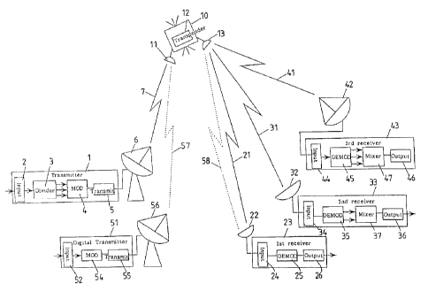
Embodiment 1
Fig. 1 shows the entire arrangement of a signal
transmission system according to the first embodiment of the
present invention. A transmitter 1 comprises an input unit 2,
a divider circuit 3, a modulat~or_~ 4, and a transmitter unit 5.
In action, each input multiplex signal is divided by the
divider circuit 3 into three groups, a first data stream D1,
a second data stream D2, a third data stream D3, which are
then modulated by the modulator 4 before transmitted from the
transmitter unit 5. 'The modulated signal is sent up from an
antennal 6 through an uplink 7 to a satellite 10 where it is
intercepted by an uplink antenna 11 and amplified by a
transponder 12 before transmitted from a downlink antenna 13
towards the ground.
The transmission signal is then sent down through three
downlinks 21, 32, and 41 to a first 23, a second 33, and a
third receiver 43 respectively. In the first receiver 23, the
24
CA 02382460 2002-05-21
~_;.
.. ..
signal intercepted by an antenna 22 is fed through an input
unit 24 to a demodulator 25 where its fir:~t data stream only
is demodulated, whale the second and third data streams are
not recovered, befor~s transmitted further from an output unit
26.
Similarly, the second receiver 33 allows the first and
second data streams of the signal intercepted by an antenna
32 and fed from an input unit 34 to be demodulated by a
demodulator 35 and then, summed by a summer 37 to a single
data stream which is then transmitted further from an output
unit 36.
The third receiver 43 allows all the first, second, and
third data streams of the signal intercepted by an antenna 42
and fed from an input unit 44 to be demodulated by a
demodulator 45 and then, summed. by a summer 47 to a single
data stream which is then transmitted further from an output
unit 46.
As understood, the three discrete receivers 23, 33, and
43 have their r~:spect:ive demodulators of different
characteristics such that their outputs demodulated from the
same frequency band signal of the transmitter 1 contain data
of different sizes. More particularly, three different but
compatible data can simultaneously be carried on a given
frequency band signal to their respective receivers. For
example, each of three, existing NTSC, HDTV, and super HDTV,
digital signals is divided into a low, a high, and a super
high frequency band components which represent the first, the
CA 02382460 2002-05-21
second, and the third data stream respectively. Accordingly,
the three different TV signals can be transmitted on a one
channel frequency band carrier for simultaneous reproduction
of a medium, a high, and a super high r~asolution TV image
respectively.
In service, the NTSC TV signal is intercepted by a
receiver accompanied with a small antenna 'or demodulation of
a small-sized data, the HDTV signal is intercepted by a
receiver accompanied with a medium antenna for demodulation
of medium-sized data, and the super HDTV signal is
intercepted by a receiver accompanied wit;h a large antenna
for demodulation of. large-sized data., Also, as illustrated
in Fig. 1, a digital NTSC TV signal containing only the first
data stream for digital NTSC TV broradcasting service is fed
to a digital transmitter 51 wherea..it is received by an input
unit 52 and modulated by a demodulator 54 before transmitted
further from a transmitter snit 55. The demodulated signal is
then sent up from an antennal 56 through an uplink 57 to the
satellite 10 which in turn transmits the same through a
downlink 58 to the first receiver 23 on t:ae ground.
The first receiver 23 demodulates with its demodulator
the modulated digital signal supplied from the digital
transmitter 51 to the original first data stream signal.
Similarly, the same modulated digital signal can be
25 intercepted and demodulated by the second 33 or third
receiver 42 to the first data stream or N'rSC TV signal. In
summary, the three discrete receivers 23, 33, and 43 all can
26
CA 02382460 2002-05-21
intercept and process a digital signal of the existing TV
system for reproduction.
The arrangement of the signal transmission system will
be described ,in more detail.
Fig. 2 is a block diagram of the transmitter 1, in which
an input signal is fed across the input unit 2 and divided by
the divider circuit 3 into three digital signals containing
a first, a second, and a third data stream respectively.
Assuming that t:he input signal is a video signal, its
IO low frequency band component is assigned to the first data
stream, its high frequency band component to the second data
stream, its super-high frequency band component to the third
data stream. The three different frequency band signals are
fed to a modulator input 61-.of thp modulator 4. Here, a
I5 signal point modu.La.ting/chariging circuit 67 modulates or
changes the positions ef the s..ignal points according to an
externally given signal. The modulator 4 is arranged for
amplitude modulation on two 90°-out-of-phase carriers
respectively which are then summed to a multiple ~M signal.
20 More specifically, the signal from the modulator input 61 is
fed to both a first 62 and a second AM modulator 63. Also, a
carrier wave of cos(2~fct) produced by a carrier generator 64
is directly fed to the first AM modulator 62 and also, to a
~/2 phase shifter 66 where it is 90° shifted in phase to a
25 sin(2nfct) form prior to transmitted to the second AM
modulator 63. The two amplitude modulated signals from the
first and second AM modulators 62, 63 are summed by a summer
27
CA 02382460 2002-05-21
65 to a transmission. signal which is then transferred to the
transmitter unit 5 for output. The procedure is well known
and will no further be explained.
The Q.A.M signal will now be described in a common 8x8 or
16 state constellation referring to the first quadrant of a
space diagram in Fi~;. 3. The output signal of the modulator
4 is expressed by a sum vector of two, Acos2~rcfct and
Bcos2nfet, vectors 81, 82 which represent the two 90°-out-of-
phase carriers respectively. When the distal point of a sum
vector from the zero point represents a signal point, the 16
QAM signal has 16 signal points determined by a combination
of four horizontal amplitude values al, az, a3, a4 and four
vertical amplitude values b1, b2, b3, b4. The first quadrant
in Fig. 3 contains four signal points 83 at Cll, 84 at C12, 85
at C22, and 86 at C~l.
C11 is a sum vector of a vector 0-al and a vector 0-bl
and thus, expressed as C11 - alcos2nfct-blsin2~fct -
Acos(2.nfct+dn/2).
It is now assumes that the distance between 0 and al in
the orthogonal coordinates of Fig. 3 is A1, between al and a2
is A2, between 0 and b1 is B1, and between b1 and bZ is BZ.
As shown in F~..g. 4, the 16 signal points are allocated
in a vector coordinate, in which each point represents a
four-bit pattern thus to allow the transmission of four bit
data per period or time slot.
Fig. 5 illustrates a common assignment of two-bit
patterns to the 16 signal points.
28
CA 02382460 2002-05-21
When the distance between two adjacent signal points is
great, it will be identified by the receiver with much ease.
Hence, it is desired to space the signal points at greater
intervals. If two particular signal points are allocated near
to each other, they are rarely distinguished and error rate
will be increased. 'therefore, it is most~preferred to have
the signal points spaced at equal intervals as shown in Fig.
5, in which the 16 QAM signal is defined by A1=AZ/2.
The transmitter 1 of the embodiment is arranged to
divide an input digital signal into a first, a second, and a
third data or bit stream. The 16 signal points or groups of
signal points are divided into four groups. Then, 4 two-bit
patterns of the first data stream are assigned to the four
signal point groups respectively, as shown in Fig. 6. More
particularly, when t:he two-bit-"pattern of the first data
stream is 11, one of four signal points of the first signal
point group 91 in the first quadrant is selected depending on
the content of the second data stream for transmission.
Similarly, when O1, one signal point of the second signal
point group 92 in the second quadrant is selected and
transmitted. When 00, one signal point of the third signal
point group 93 in the third quadrant is transmitted and when
10, one signal point of the fourth signal point group 94 in
the fourth quadrant is trarismitted. Also, 4 two-bit patterns
in the second data stream of the 16 QAM :signal, or e.g. 16
four-bit patterns in the second data stream of a 64-state QAM
signal, are assigned to four signal points or sub signal
29
CA 02382460 2002-05-21
point groups of each of the four signal point groups 91, 92,
93, 94 respectively, as shown in Fig. 7. It should be
understood that the assignment is symmetrical between any two
quadrants. The assignment of the signal points to the four
groups 91, 92, 93, 94 is determined by priority to the two-
bit data of the first data stream. As the result, two-bit
data of the first data stream and two-bit data of the second
data stream can be transmitted independently. Also, the first
data stream will be demodulated with the use of a common 4
PSK receiver having a given antenna sensitivity. If the
antenna sensitivity is higher, a modified type of the 16 7f~M
receiver of the present invention will intercept and
demodulate both the first and second data stream with equal
success.
Fig. 8 shows an example~v~of.the assignment of the first
and second data streams in two.-bit patterns.
When the low frequency band component of an HDTV video
signal is assigned to the first data stream and the high
frequency component to the second data stream, the 4 PSK
receiver can produce an NTSC-level picture from the first
data stream and the 16- or 64-state QAM receiver can produce
an HDTV picture from a composite reproduction signal of the
first and second data streams.
Since the signal points are allocated at equal
intervals, there is developed in the 4 PSK receiver a
threshold distance between the coordinate axes and the shaded
area of the first quadrant, as shown in. Fig. 9. If the
CA 02382460 2002-05-21
threshold distance is A,1,Q, a PSK signal having an. amplitude
of A~ will successfully be intercepted. However, the
amplitude has to be increased to a three times greater value
or 3A~ for transmission of a 16 QAM signal while the
threshold distance A,~ being maintained. More particularly,
the energy for transmitting the 16 ~I signal is needed nine
times greater than that for sending the 4 PSK signal. Also,
when the 4 PSK signal is transmitted in a 16 QAM mode, energy
waste will be high and reproduction of a carrier signal will
be troublesome. Above all, the energy available for satellite
transmitting is not ,abunda.nt but strictly limited to minimum
use. Hence, no large-energy-consuming signal transmitting
system will be put into practice until more energy for
satellite transmission is available. It is expected that a
great number of the 4 PSK rzce;i-vers are introduced into the
market as digital TV broadcasting is soon in service. After
introduction to the market, the 4 PSK receivers will hardly
be shifted to higher sensitivity models because a signal
intercepting characteristic gap between the two, old and new,
models is high. Therefore, the transmission of the 4 PSK
signals must not be abandoned.
In this respect, a new system is desperately needed for
transmitting the signal point data of a quasi 4 PSK signal in
the 16 1C,~M mode with. the use of less energy. Otherwise, the
limited energy at a satellite station will degrade the entire
transmission.system.
The present invention resides in a multiple signal level
31
CA 02382460 2002-05-21
arrangement in which the four signal point groups 91, 92, 93
94 are allocated at a greater distance from each other, as
shown in Fig. 10, for minimizing the energy consumption
required for 16 ~'yI modulation of quasi 4 PSK signals.
For clearing the relation between the signal receiving
sensitivity and the transmitting energy, the arrangement of
the digital transmitter 51 and the first receiver 23 will be
described in more detail referring to Fig'. 1.
Both the digital transmitter 51 and the fist receiver 23 are
formed of known types for data transmission or video signal
transmission e.g. in TV broadcasting service. As shown in
Fig. 17, the digital transmitter 51 is a 4 PSK transmitter
equivalent to the multiple-bit e.AM transmitter 1, shown in
Fig. 2, without AM modulation capability. In operation, an
input signal is fed through an=input unit 52 to a modulator
54 where it is divided by a~-modulator input IZI to two
components. The two components are then transferred to a
first two-phase modulator circuit 122 for phase modulation of
a base carrier and a second two-phase modulator circuit 123
for phase modulation of a carrier which is 90° out of phase
with the base carrier respectively. Two outputs of the first
and second two-phase modulator circuits 122, 123 are then
summed by a summer 65 to a composite modulated signal which
is further transmitted from a transmitter unit 55.
The resultant modulated signal is shown in the space
diagram of Fig. 18.
It is known that the four signal points are allocated at
32
CA 02382460 2002-05-21
equal distances for achieving optimum energy utilization.
Fig. 18 illustrates an example where the four signal points
125, 126, 127, 128 represent 4 two-bit patterns, 11, 01, 00,
and 10 respectively.. It is also desired for successful data
transfer from the digital transmitter 51 to the first
receiver 23 than the 4 PSK signal from the digital
transmitter 51 has an amplitude of not less than a given
level. More specifically, when the minimum amplitude of the
4~ PSK signal needE:d for transmission from the digital
transmitter 51 to the first receiver 23 of 4 PSK mode, or the
distance between 0 and al in Fig. 18 is A,i,~, the first
receiver 23 successfully intercept any 4 PSK signal having an
amplitude of more than A,j,O.
The first receiver 23 is arr,a.nged to receive at its
small-diameter antenna 22 a de si.ned or 4 F'SK signal which is
transmitted from the transmitter 1 or digital transmitter 51
respectively through. the transponder 12 of the satellite 10
and demodulate it with the demodulator 24. In more
particular, the first receiver 23 is substantially designed
for interception of a digital TV or data communications
signal of 4 PSK or 2 PSK mode.
Fig. 19 is a block diagram of the first receiver 23 in
which an input signf~.l received by the antenna 22 from the
satellite 12 is fed through the input unit 24 to a carrier
reproducing circuit 131 where a carrier wave is demodulated
and to a ~c/2 phase shifter 132 where a 90° phase carrier wave
is demodulated. Also, two 90°-out-of-phase components of the
33
CA 02382460 2002-05-21
input signal are detected by a first 133 and a second phase
detector circuit 134 respectively and transferred to a first
136 and a second d.iscrimination/demodulation circuit 137
respectively. Two demodulated components from their
respective discrimination/demodulation circuits 136 and 137,
which have separately been discriminated at units of time
slot by means of timing signals from a timing wave extracting
circuit 135, are fed to a first data stream reproducing unit
232 where they are summed to a first data stream signal which
is then delivered as an output from the output unit 26.
The input signal to the first recei'Ter 23 will now be
explained in more detail referring to the vector diagram of
Fig. 20. The 4 PSK signal received by the first receiver 23
from the digital transmitter 51 is expressed in an ideal form
without transmission distortion end noise, using four signal
points 151, 152, 153, 154 shown in Fig. 20.
In practice, the real four~signal points appear in
particular extended areas about the ideal signal positions
151, 152, 153, 154 respectively due to noise, amplitude
distortion, and phase error developed during transmission. If
one signal point is unfavorably displaced from its original
position, it will hardly be distinguished. from its ,neighbor
signal point and the error rate will thus be increased. As
the error rate increasfas to a critical Ievel, the
reproduction of data becomes less accurate. For enabling the
data reproduction at a maximum acceptable level of the error
rate, the distance between any two signa:~_ points should be
34
CA 02382460 2002-05-21
=-" ...
far enough to be distinguished from each other. If the
distance is lA~, the signal point 151 of a 4 PSK signal at
close to a critical error level has t;o stay in a first
discriminating area 155 denoted by the hatching of Fig. 2G
and determined by ~0-a~~_>.A~ and ~0-b~~?A~. This allows the
signal transmission. system to reproduce carrier waves and
thus, demodulate a wanted signal. When the minimum radius of
the antenna 22 is set to r~, the transmission signal of more
than a given level can be intercepted by any receiver of the
system. The amplitude of. a 4 F'SK signal of the digital
transmitter 51 shown in Fig. 18 is minimum at A~ and thus,
the minimum amplitude A~ of a 4 PSK signal to be received by
the first receiver 23 is determined equal to A,I,~. As the
result, the first receiver 23 can~intercept and demodulate
the 4 PSK signal from the digital trarasmitter 51 at the
maximum acceptable level of the error rate when the radius of
the antenna 22 is more than r~. If the transmission signal is
of modified 16- or fi4-state ca,4M mode, the first receiver 23
may find difficult to reproduce its carrier wave. For
compensation, the signal points are incre.~,sed to eight which
are allocated at angles of (n/4+nn/2) as shown in Fig. 25(a)
and its carrier wave will be reproduced by a 16x
multiplication technique. Also, if the signal points are
assigned to 16 locations at angles of nnj8 as shown in Fig.
25(b), the carrier ~of a quasi 4 PSK mode 16 QAM modulated
signal can be reproduced with the carrier reproducing circuit
131 which is modified for performing 16x frequency
CA 02382460 2002-05-21
multiplication. At the time, the signal points in the
transmitter I should be arranged to satisfy
AL/(Al+AZ)=tan(n/8) .
Here, a case of receiving a QPSK signal will be
considered. Similarly to the manner performed by the signal
point modulating/changing circuit 67 in the transmitter shown
in Fig. 2, it is also possible to modulate the positions of
the signal points of the QPSK signal shown in Fig. 18
(amplitude-modulation, pulse-modulation, or the like). In
this case, the signal point demodulating unit I38 in the.
first receiver 23 demodulates the gosition modulated or
position changed signal. The demodulated signal is outputted
together with the first data stream.
The 16 PSK signal of the transmitter 1 will now be
explained referring to the vector diagram of Fig. 9. When
the horizontal vector distance.Al of the signal point 83 is
greater than A,I,~ of t:he minimum amplitude of the 4 PSK signal
of the digital transmitter 51, the four signal points 83, 84,
85, 86 in the first quadrant of Fig. 9 stay in the shaded or
first 4 PSK signal receivable area 87. When received by the
first receiver 23, the four points of the signal appear in
the first discriminating area of the vector field shown in
Fig. 20. Hence, any of the signal points 83, 84, 85, 86 of
Fig. 9 can be translated into the signal level 151 of Fig. 20
by the first receiver 23 so that the two-bit pattern of 11 is
assigned to a corresponding time slot. The two-bit pattern
of I1 is identical to I1 of the first signal point group 91
36
CA 02382460 2002-05-21
or first data stream of a signal from the transmitter 1.
Equally, the first data stream will be reproduced at the
second, third, or fourth quadrant. As them result, the first
receiver 23 reproduces two-bit data of the first data stream
out of the pluralit;~ of data streams in a 16-, 32-, or 64-
state ~M signal transmitted from the transmitter 1. The
second and third data streams are contained in four segments
of the signal point group 01 and thus, will not affect on the
demodulation of the first data stream. They may however
affect the reproduction of a carrier wave and an adjustment,
described later, will be needed.
If the transpander of a satellite supplies an abundance
of energy, the forgoing technique of 16 to 64-state RAM mode
transmission will be feas:ibl~e. However, the transponder of
the satellite in any existing satellite transmission system
is strictly limited in the power supply due to its compact
size and th_e capability of solar batteries. If the
transponder or satellite is increased in size thus weight,
its launching cost will soar. This disadvantage will rarely
be eliminated by traditional techniques unless the cost of
launching a satelliv~e rocket is reduced to a considerable
level. In the existing system, a common communications
satellite provides as low as 20 W of power supply and a
common broadcast satellite offers :100 W to 200 W at best. For
transmission of such a 4 PSK signal in the symmetrical 16-
state 1~.M mode as shown in Fig. 9, the minimum signal point
distance is needed 3..4,~ as the 16 RAM amplitude is expressed
37
CA 02382460 2002-05-21
by 2A1=AZ. Thus, the: energy needed for the purpose is nine
times greater than that for transmission of a common 4 PSK
signal, in order to maintain compatibility. Also, any
conventional satellite transponder can hardly provide a power
for enabling such a ;small antenna of the 4 PSK first receiver
to intercept a transmitted. signal therefrom. For example, in
the existing 40W system, 360W is needed for appropriate
signal transmission and will be unrealistic in the respect. of
c~o s t .
It would be under stood that the symmetrical signal
state GZAM technique is most effective when the receivers
equipped with the same sized antennas are employed
corresponding to a given transmitting power. Another novel
technique will however bew preferred for use with the
receivers equipped with diff'eren,.t sized antennas.
In more detail, while.-the 4 PSK signal can be
intercepted by a common low cost receiver system having a
small antenna, the 16 QAM signal is intended to be received
by a high cost, high quality, multiple-bit modulating
receiver system with a medium or large sized antenna which is
designed for providing highly valuable services, e.g. HDTV
entertainments, to a particular person who invests more
money. This allows both 4 PSK and 16 QAM signals, if desired,
with a 64 DMA, to be transmitted. simultaneously with the help
of a small increase in the transmitting power.
For example, th.e transmitting power can be maintained
low when the signapoints are allocated at Al= AZ as shown
38
CA 02382460 2002-05-21
in Fig. 10. The amplitude A(4) for transmission of 4 PSK data
is expressed by a vector 96 equivalent to a square root of
(A1+AZ)Z+(B1+B2)Z. Then,
A ( 4 ) ~ ~=A1Z+Bl~=A,r6Z+A,j,~~=2A1,62
~ A ( I 6 ) ~ 2= (A1+A~) Z+ ( B1+BZ ) ~4A,1,02+4A,j,D~=8,1,62
~A(16)I/~A(4)I==2
Accordingly, the 16 QAM signal can be transmitted at a
two times greater amplitude and a four times greater
transmitting energy than those needed for the 4 PSK signal.
A modified 16 Q~-1M signal according to the present invention
will not be demodulated by a common receiver designed for
symmetrical, equally distanced signal poizit QOM. However, it
can be demodulated with the second receiver 33 when two
threshold A1 and AZ are predetermined to appropriate values.
At Fig. 10, the minimum distance between two signal points in
the first segment of the signal :point group 91 is A1 and
AZ/2A1 is established as campared with the distance 2A1 of 4
PSK: Then, as A1=AZ, the distance becomes 1/2. This explains
that the signal receiving sensitivity has to be two times
greater for the same error. rate and four times greater for
the same signal level. For having a four times greater value
of sensitivity, the radius r2 of the antenna 32 of the second
receiver 33 has to be two times greater than the radius r1 of
the antenna 22 of the first receiver 23 thus satisfying
r2=2r~. For example, the antenna 32 of the second receiver 33
is 60 cm diameter when the antenna 22 if the first receiver
23 is 30 cm. In this manner, the second data stream
39
CA 02382460 2002-05-21
representing the high frequency component of an HDTV will be
carried on a signal channel and demodulated successfully. As
the second receiver 33 intercepts the second data stream or
a higher data signal, its owner can enjoy a return of high
investment. Hence, the second receiver 33 of a high price may
be accepted. As the minimum energy for transmission of 4 PSK
data is predetermined, the ratio nifi of modified 16 APSK
transmitting energy to 4 PSK transmitting energy will be
calculated to the antenna radius r2 of the second receiver 33
using a ratio between A~ and AZ shown in Fig. 10.
In particular, nls is expressed by ( (A1+AZ)/A1)Z which is
the minimum energy for transmission of 4 PSK data. As the
signal point distance suited for modified 16 6,lAM interception
is AZ, the signal point distance fQr 4 PSK interception is
2A1, and the signal goint di:.s.~ance ratio is AZ/2A1, the
antenna radius rZ is determined_as shown in Fig. 11, in which
the curve 101 represents the relation between the
transmitting energy ratio n16 and the radius r~ of the antenna
22 of the second receiver 23.
Also, the point lOZ indicates transmission of common 16
QAM at the equal distance signal state mode where the
transmitting energy is nine times greate:c and thus will no
more be practical. Aa apparent from the graph of Fig. 11, the
antenna. radius r2 of the second receiver 23 cannot be reduced
further even if nls is increased more than 5 times.
The transmitting energy at the satellite is limited to
a small value and thus, n1b preferably stays not more than 5
~0
CA 02382460 2002-05-21
times the value, as denoted by the hatching of Fig. 11. The
point 104 within the hatching area 103 indicates, for
example, that the antenna radius r2 of a two times greater
value is matched with a 4x value of the transmitting energy.
Also, the point 105 represents that the transmission energy
should be doubled when r2 is about 5x greater. Those values
are all within a feasible range.
The value of nls not greater than 5x value is expressed
using A1 and AZ as:
nls = ( (Al+AZ ) /Al) Z<_ 5
Hence, AZ<-1.23A1.
If the distance between any two signal point group
segments shown in Fi~;. 10 is 2A(4) and the maximum amplitude
is 2A(16) , A(4) and A(16)-.4(4) are proportional to Ai and AZ
respectively. Hence, (A(16):)2~5(A(14))Z is established.
~ The action of a modifiedv.64 ASPK transmission will be
described as the third receiver 43 can perform 64-state Q~1M
demodulation.
Fig. 12 is a vector diagram in which each signal point
group segment contains 16 signal points as compared with 4
signal points of Fi.g. 10. The first signal point group
segment 91 in Fig. 12 has a 4x4 matrix of 16 signal points
allocated at equal intervals including the point 170. For
providing compatibility ~,~ith 4 PSK, A1-'>A.~ has to be
satisfied. If the radius of the antenna 42 of the third
receiver 43 is r3 and the transmitting energy is n~, the
equation is expressed as:
41
CA 02382460 2002-05-21
r32 = {6Z/ ~w1) }rlZ
This relation between r3 and n of a. 64 QpM signal is
also shown in the graphic representation of Fig. 13.
It is under stood that the signal point assignment shown
in Fig. 12 allows the second receiver 33 to demodulate only
two-bit patterns of 4 PSK data. Hence, it is desired for
having compatibility between the first, second, and third
receivers that the second receiver 33 is arranged capable of
demodulating a modified 16 9AM form from the 64 ~IA.M modulated
1.0 signal.
The compatibility between the three discrete receivers
can be implemented by three-level grouping of signal points,
as illustrated in Fig. 14. The description will be made
referring to the fi:cst quadrant in whicr the first signal
point group segment 91 represents the two-bit pattern 11 of
the first data stream.
In particular, a first sub segment 181 in the. first
signal point group segment 91 is assigned the two-bit pattern
11 of the second data stream. Equally, a second 182, a third
183, and a fourth sub segment 184 are assigned O1, 00, and 10
of the same respectively. This assignment is identical to
that shown in Fig. 7.
The signal poir~.t allocation of the third data stream
will now be explained referring to the vector diagram of Fig.
15 which shows the first quadrant. As shown, the four signal
points 201, 205, 209, 213 represent the t;wo-bit pattern of
11, the signal points 202, 206, 210, 214 represent 01, the
42
CA 02382460 2002-05-21
signal points 203, 207, 211, 215 represent 00, and signal
points 204, 208, 21.2, 216 represent 10. Accordingly, the
two-bit patterns of the third data stream can be transmitted
separately of the first and second data streams. In other
words, two-bit data of the three different signal levels can
be transmitted respE:ctively.
As understood, the present invention permits not only
transmission of six-bit data but also intE~rception of three,
two-bit, four-bit, and si.x-bit, different bit length data
with their respective receivers while the signal
compatibility remains between three levels.
The signal point allocation for prov;_ding compatibility
between the three levels will be described.
As shown in Fig.. 15, Al?A,~ is essenti,~.l for allowing the
first receiver 23 to receiver'~the..first data stream.
It is needed to space any two signal points from each
other by such a distance that the sub segment signal points,
e.g. 182, 183, 184, of the second data stream shown in Fig.
15 can be distinguished from the signal point 91 shown in
Fig. 10.
Fig. 15 shows that they are spaced by 2/3A2. In this
case, the distance between the two signal points 201 and 202
in the first sub segment 181 is AZ/6. The transmitting energy
needed for signal ini~erception with the tl:_ird receiver 43 is
now calculated. If the radius of the antenna 32 is r3 and the
needed transmitting energy is n~ times the 4 PSK transmitting
energy, the equation is expressed as:
43
CA 02382460 2002-05-21
r3Z= ( 12 r1) Z/ ( n-1 )
This relation is also denoted by the curve 211 in Fig. 16.
For example, if the transmitting energy is 6 or 9 times
greater than that for 4 PSK transmission at the point 223 or
222, the antenna 32 having a radius of 8x or 6x value
respectively can intercept the first, second, and third data
streams for demodulation. .4s the signal point distance of the
second data stream is close to 2/3AZ, the relation between r1
and r2 is expressed by:
r22=( 3r1)2/ (n-1)
Therefore, the antenna 32 of the second receiver 33 has to be
a little bit increased in radius as denoted by the curve 223.
As understood, while the first and second data streams
are transmitted trough a traditional; satel Lite which provides
a small signal transmitting energy, the third data stream can
also be transmitted through a future satellite which provides
a greater signal transmitting energy without interrupting the
action of the first and second receivers 23, 33 or with no
need of modification of the same and thus, both the
compatibility and t;he advancement will highly be ensured.
The signal receiving action of the second receiver 33
will first be descrilaed. As compared with the first receiver
23 arranged for interception with a small radius r1 antenna
and demodulation of t;he 4 PSK modulated signal of the digital
transmitter 51 or the first data stream of the signal of the
transmitter 1, the second receiver 3?, is adopted for
perfectly demodulating the 16 signal ,state two-bit data,
44
CA 02382460 2002-05-21
,.. ..... ., ~ ..
shown in Fig. 10., or second data stream of the 16 4AM signal
from the transmitter 1. In total, four--bit data including
also the first data stream can be demodulated. The ratio
between A1 and AZ is however different in the two
transmitters. The two different data are loaded to a
demodulation controller 231 of the second. receiver 33, shown
in Fig. 21, which in turn supplies their respective threshold
values to the demodulating circuit for A~'~I demodulation.
The block diagram of the second receiver 33 in Fig. 21
is similar in basic construction to that of the first
receiver 23 shown in Fig. 19. The difference is that the
radius r2 of the antenna 32 is greater than r1 of the antenna
22. This allows the second receiver 33 to identify a signal
component involving a smaller signal point distance. The
demodulator 35 of the second:r~ceiver 33 also contains a
first 232 and a second data stream reproducing unit 233 in
addition to the demodulation controller 231. There is
provided a first discrimination/reproduction circuit 136 for
AM demodulation of modified 16 QAM signals. As understood,
each carrier is a four-bit signal having two, positive and
negative, threshold values about the zero level. As apparent
from the vector diagram, of Fig. 22, the threshold values are
varied depending on the transmitting energy of a transmitter
since the transmitting signal of the embodiment is a modified
16 QArI signal. When. the reference threshold is TH16, it is
determined by, as shown i:n Fig. 22:
TH16 = ( Al+AZ / 2 ) / ( A1+A~ )
CA 02382460 2002-05-21
The various data for demodulation including A1 and AZ or
TH16, and the value m for multiple-bit modulation are also
transmitted from the transmitter 1 as curried in the~first
data stream. The demodulation controller 231 may be arranged
for recovering such demodulation data through statistic
process of the received signal.
A way of determining the shift factor A1/AZ will be
described with reference t.o Fig. 26. A change of the shift
factor A1/AZ causes t~ change of the threshold value. Increase
of a difference of a values of Al/AZ set at the receiver side
from a value of Al/AZ set at the transmitter side will
increase the error rate. Referring to Fig. 26, the
demodulated signal from the second data stream reproducing
unit 233 may be fed back to the demodulation controller 231
to change the shift factor Al/AZ' in a direction to increase
the error rate. By this arrangement, the third receiver 43
may not demodulate the shift factor A1/AZ, so that the circuit
construction can be simplified. Further, the transmitter may
not transmit the shift factor A1/A~, so that the transmission
capacity can be increased. This technique can be applied also
to the second receiver 33.
Figs. 25(a) and 25(b) are views showing signal point
allocations for the C-CDM signal points, wherein signal
points are added by shifting in the polar coordinate
direction (r, A). The previously described C-CDM is
characterized in that the signal points are shifted in the
rectangular coordinate direction, i.e. XY direction;
46
CA 02382460 2002-05-21
therefore it is referred to as rectangular coordinate system
C-CDM. Meanwhile, this C-CDM characterized by the shifting
of signal points in the polar coordinate direction, i.e. r,
8 direction, is referred to as polar coordinate system C-CDM.
Fig. 25(a) shows the signal allocation of 8PS-APSK
signals, wherein tour signal points are added by shifting
each of 4 QPSK signals in the radius r direction of the polar
coordinate system. In this manner, the APSK of polar
coordinate system C--CDM having 8 signal points is obtained
from the QPSK as shown in Fig. 25(a). As the pole is shifted
in the polar coordinate system to add signal points in this
APSK, it is referred. to as shifted pole-APSK, i.e SP-APSK in
the abbreviated form.. In this case, coordinate value of the
newly added four QPSK signals 85 are specified by using a
shift factor S1 as shown in. Fi'g.-'139. Name.'.y, 8PS-APSK signal
points includes an ordinary QPSK signal points 83 (r0, 8~) and
a signal point ((S~,+:l)r~, E~Q) obtained by shifting the signal
point 83 in the radius r direction by an amount of Slr~.
Thus, a 1-bit sub channel 2 is obtained in addition to a 2-bit
subchannel 1 identical with the QPSK.
Furthermore, as; shown in the constellation diagram of
Fig. 140, new eight signal points, represented by coordinates
( r~+SZr~, 8~) and ( r~~-SlrO+SGrp, A~ ) , can be added by shi f t ing
the eight signal points (r~, A~)and (rQ+SlrO, 6~) in the radius
r direction. As this allows two kinds of a7.locations, a 1-bit
subchannel is obtained and is referred to as 16PS-APSK which
provides the 2-bit subchar~nel 1, L-bit subchannel 2, and 1-
47
CA 02382460 2002-05-21 '°
bit subchannel 3. As the 16-PS-APSK disposes the signal
points on the lines of 8=1/4~(2n+1)n, it allows the ordinary
QPSK receiver explained with reference to Fig. 19 to
reproduce the carrier wave to demodulate the first subchannel
of 2-bit although the second subchannel cannot be
demodulated. As described above, the C-CDM method of
shifting the signal points in the polar coordinate direction
is useful in expanding the capacity of information data
transmission while assuring compatibility to the PSK,
especially to the C,~PSK receiver, a main receiver for the
present satellite broadcast service. Therefore, without
losing the first generation viewers of the satellite
broadcast service based on the PSK, the broadcast service
will advance to a second generation stage wherein the APSK
will be used to increase trari'smiLtable inr.'ormation amount by
use of the multi.-level modulation while maintaining
compatibility.
In Fig. 25(b), the signal points are allocated on the
lines of 6=~/8. With this arrangement, the 16 PSK signal
points are reduced or limited to 12 signal points, i.e. 3
signal points in each quadrant. With this limitation, these
three signal points in each quadrant are roughly regarded as
one signal point for 4 QPSK signals. Therefore, this
enables the QPSK receiver to reproduce tb.e first subchannel
in the same manner as in the previous embodiment.
More specifically, the signal points are disposed on the
lines of 8=n/4, 8=n/4+n/8, and 8=n/4-n/8. In other words,
48
CA 02382460 2002-05-21
the added signals are offset by an amount ~8 in the angular
direction of the polar coordinate system from the QPSK
signals disposed on the lines of 8=~/~~. Since all the
signals are in the range of 8=n/4~~/8, they can be regarded
as one of QPSK signal points on the line of A=n/4. Although
the error rate is lowered a little bit in this case, the QPSK
receiver 23 shown in Fig. 1.9 can discriminate these points as
four signal points a:ngularly allocated. Thus, 2-bit data can
be reproduced.
In case of the angular shift C-CDM, if signal points are
disposed on the lines of n/n, the carrier wave reproduction
circuit can reproduce the carrier wave by the use of an n-
multiplier circa it in the same manner as in other
embodiments. If. they signal ~points,are not disposed on the
lines of n/n, the carrier' wave can be reproduced by
transmitting several carrier .,information within a
predetermined period in the same manner as in other
embodiment.
Assuming that an angle between two signal points of the
QPSK or 8-SP-APSK is 26~ in the polar coordinate system and
a first angular shift factor is P1, two signal points (r~,
Ap+P100) and (r~, 6~-F'16~) are obtained by shifting the QPSK
signal point in the angular 8 direction by an amount ~P160'
Thus, the number of signal points are doubled. Thus, the 1
bit subchannel 3 can be added and is referred to as 8-SP-PSK
of P=P1. If eight signal points are further added by
shifting the 8-SP-PSK signals in the radiu:~ r direction by an
49
CA 02382460 2002-05-21
amount Slr~, it will become possible to obtain 16-SP-APSK (1?,
Sl type) as shown iri Fig. 142. The subchannels 1 and 2 can
be reproduced by two 8PS-PSKs having the same phase with each
other. Returning to Fig. 25(b), as the C-CDM based on the
angular shift in the polar coordinate sy:~tem can be applied
to the PSK as shown in Fig. 141, this will be adopted to the
first generation satellite broadcast service. However, if
adopted to the second generation satellite broadcasting based
on the APSK, this polar coordinate system C-CDM is inferior
in that signal points in t;he same group cannot be uniformly
spaced as shown i:n Fig. 142. Accordingly, utilization
efficiency of electric power is worsened. On the other hand,
the rectangular coordinate system C-CDM has good
compatibility to the PSK.
The system shown in Fig. 25~(b) is compatible with both
the rectangular and polar coordinate systems. As the
signal points are disposed on the angular lines of the 16
PSK, they can be demodulated by the 16 PSK. Furthermore, as
the signal points are divided into groups, the QPSK receiver
can be used for demodulation. Still further, as the signal
points are also allocated to suit for' the rectangular
coordinate system, the demodulation will be performed by the
16-SRQAM. Consequently, the compatibi7.ity between the
rectangular coordinate system C-CDM and the polar coordinate
system C-CDM can be assured in any of the QPSK, 16PSK, and
16-SRQAM.
The demodulati.o:n controller 231 has a memory 231a for
CA 02382460 2002-05-21
storing thereiw different threshold values (.i.e., the shift
factors, the number of signal points, the synchronization
rules, etc.) which correspond to different channels of TV
broadcast. When receiving one of the channels again, the
values corresponding to the receiving channel will be read
out of the memory to thereby stabilize the reception quickly.
If the demodulation data is lost, the demodulation of
the second data stream will hardly be exe~~uted. This will be
explained referring to a flow chart shown in Fig. 24.
Even if the demodulation data ws not available,
demodulation of the 4 PSK at Step 313 and of the first data
stream at Step 301 can be implemented. At Step 302, the
demodulation data retrieved by the i-.'irst data stream
reproducing unit 232 is transferred to the demodulation
controller 231. If m is 4 or-2 ,a~.. Step 30:3, the demodulation
controller 231 triggers demodulation of 4 PSK or 2 PSK at
Step 3I3. If not, the procedure moves to Step 310. At Step
305, two threshold values TH8 and TH16 are calculated. The
threshold value THis for Ai~t demodulation is fed at Step 306
from the demodulation controller 231 to both the first 136
and the second discrimination/reproduction circuit 137.
Hence, demodulatian of the modified 16 6iAM signal and
reproduction of the second data stream can be carried out at
Steps 307 and 315 respectively. At Step .308, the error rate
is examined and if high, the procedure returns to Step 313
for repeating the 4 PSK demodulation.
As shown in Fig. 22, the signal points 85, 83, are
51
CA 02382460 2002-05-21
aligned on a line at an angle of cos(~t+nn/2) while 84 and 86
are off the line. Hence, the feedback of a second data
stream transmitting carrier wave data from the second data
stream reproducing unit 233 to a carrier reproducing circuit
131 is carried out so that no carrier needs to be extracted
at the timing of the: signal points 84 and 86.
The transmitter 1 is arranged to transmit carrier timing
signals at intervals of a given time with the first data
stream for the purpose of compensation for no demodulation of
the second data stream. The carrier timing signal enables to
identify the signal points 83 and 85 of the first data stream
regardless of demodulation of the second data stream. Hence,
the reproduction of carrier wave can be triggered by the
transmitting carrier data 'to-the carrier reproducing circuit
131.
It is then examined at Step 304 of the flow chart of
Fig. 24 whether m is 16 or not upon receipt of such a
modified 64 Q,AM signal as shown in Fig. 23. At Step 310, it
is also examined whether m is more than 64 or not. If it is
determined at Step 311 that the received signal has no equal
distance signal point constellation, the procedure goes to
Step 312. The signal point distance THE of the modified 64
Q~I signal is calculated from:
THE _ ( AI+AZ / 2 ) / ( Al+AZ )
This calculation is equivalent to that of 'rHls but its
resultant distance between signal points is smaller.
If the signal point distance in the first sub segment
52
CA 02382460 2002-05-21
181 is A3, the distance between the first 181 and the second
sub segment 182 is expressed by (A2 2A3). Then, the average
distance is (AZ-2A~),/(Al+A~) which is designated as due. When
d~ is smaller than T2 which represents the signal point
discrimination capability of the second receiver 33, any two
signal points in th.e segment will hardly be distinguished
from each other. This judgement is executed at Step 313. If
d~ is out of a permissive range, the procC~dure moves back to
Step 313 for 4 PSK mode demodulation. I:E d~ is within the
range, the procedure advances to Step 305 for allowing the
demodulation of 16 ~~M at Step 307. If it is determined at
Step 308 that the error rate is too high, the procedure goes
back to Step 313 for' 4 PSK mode demodulation.
When the transmitter 1 supplied a modified 8 QAM signal
such as shown in Fib;. 25 (a) ~'in. which all the signal points
are at angles of cos(2~f+n~n/4), the carrier waves of the
signal are lengthened to the same phase and will thus be
reproduced with much. ease. At the time, two-bit data of the
first data stream are demodulated with -the 4-PSK receiver
while one-bit data of the second data stream is demodulated
with the second receiver 33 and the total of three-bit data
can be reproduced.
The third receiver 43 will be described in more detail.
Fig. 26 shows a block diagram of the third receiver 43
similar to that of the second receiver 33 in Fig. 21. The
difference is that a third data stream reproducing unit 234
is added and also, the discrimination/reproduction circuit
53
CA 02382460 2002-05-21
has a capability of identifying eight-bit data. The antenna
42 of the third receiver 43 has a radius r3 greater than rZ
thus allowing smaller distance state signals, e.g. 32- or 64-
statef~AM signals, to be demodulated. For demodulation of the
64 QAM signal, the first discrimination/reproduction circuit
136 has to identify 8 digital levels of the detected signal
in which seven different threshold levels are involved. As
one of the threshold values is zero, thrE:e are contained in
the first quadrant.
Fig. 27 shows a space diagram of the signal in which the
first quadrant contains three different threshold values.
As shown in Fig. 27, when the three normalized threshold
values are TH1~, TH2~,. and TH3~, they are expressed by:
TH1~ _ (Al+A3/2 ) / (Al+A.Z)
TH2~ _ (A1+AZ/ 2 ) / (Al+AZ ) aid
TH3~ _ (Al+AZ-A~/2 ) / (Al+AZ)v. ,
Through AM demodulation of a phase detected signal using
the three threshold values, the third data stream can be
reproduced like the first and second data stream explained
with Fig. 21. The third data stream contains e.g. four
signal points 201, 202, 203, 204 at the first sub segment 181
shown in Fig. 23 wh.ic:h represent 4 values of two-bit pattern.
Hence; six digits or modified 64 6.7Arf signals can be
demodulated.
The demodulation controller 231 detects the value m, Al,
A2, and A3 from the demodulation data contained in the first
data stream demodulated at the first data stream reproducing
54
CA 02382460 2002-05-21
unit 232 and calculates the three threshold values TH1~,
TH2~, and TH3~ which are then fed to the first 136 and the
second discrimination/reproduction circuit 137 so that the
modified 64 QAM sign;s.l is demodulated with certainty. Also,
if the demodulation data have been scrambled, the modified 64
QAM signal can be demodulated only with a specific or
subscriber receiver. Fig. 28 is a flow chart showing the
action of the demodulation controller 231 :for modified 64 7f,~M
signals. The difference from the flow chart for demodulation
of 16 QOM shown in Fig. 24 will be explained. The procedure
moves from Step 304 to Step 320 where it is examined whether
m=32 or not. If m=32, demodulation of ;32 Q~I signals is
executed at Step 322. If not, the procedure moves to Step 321
where it is examined whether- m=64: or not. If yes, A3 is
examined at Step 323. If A3 i's~smaller than a predetermined
value, the procedure moves to Step 305 and the same sequence
as of Fig. 24 is implemented. If it is ;;udged at Step 323
that A3 is not smaller than the predetermined value, the
procedure goes to Step 324 where the threshold values are
calculated. At Step 325, the calculated threshold values are
fed to the first and second discrimingtion/reproduction
circuits and at Step 326, the demodulation of the modified 64
6ZAM signal is carried out. Then, the first, second, and third
data streams are reproduced at Step 327. At Step 328, the
error rate is examined. If the error rate is high, the
procedure moves to Step 305 where the 16 QAM demodulation is
repeated and if low, the demodulation of the 64 4AM is
CA 02382460 2002-05-21
continued.
The action of carrier wave reproduction needed for
execution of a satisfactory demodulating procedure will now
be described. The scope of the present invention includes
reproduction of the first data stream of a modified 16 or 64
6?AM signal with t.he: use of a 4 PSK receiver. However, a
common 4 PSK receiver rarely reconstructs carrier waves, thus
failing to perform a correct demodulation. For compensation,
same arrangements are necessary at both the transmitter and
receiver sides.
Two techniques for the compensation are provided
according to the present invention. A first technique relates
to transmission of signal points aligned at angles of (2n-
1)n/4 at intervals of a given. time. A second technique offers
transmission of signal points,,arranged at intervals of an
angle of nn/8.
According to the first technique, the eight signal
points including 83 and 85 are aligned at angles of n/4,
3n/4, 5n/4, and 7n/4, as shown in Fig. :.8. In action, at
least one of the eight signal points is transmitted during
sync time slot periods 452, 453, 454, 455 arranged at equal
intervals of a time in a time slot gap 451 shown in the time
chart of Fig. 38. Any desired signal points are transmitted
during the other time slots. The transmitter 1 is also
arranged to assign a data for the time slot interval to the
sync timing data region 499 of a sync data block, as shown in
Fig. 41.
56
CA 02382460 2002-05-21
f - ,;.
The content of a transmitting signal will be explained
in more detail referring to Fig. 41. The rime slot group 451
containing the sync time slots 452, 453, 454, 455 represents
a unit data stream or block 491 carrying a data of Dn.
The sync time slots in the signal are arranged at equal
intervals of a given time determined by the time slot
interval or sync timing data. Hence, when the arrangement of
the sync time slots is detected, reproduction of carrier
waves will be executed slot by slot through extracting the
sync timing data from their respective time slots.
Such a sync timing data S is contained i;.1 a sync block 493
accompanied at the front end of a data frame 492, which is
consisted of a number of the sync time slots denoted by the
hatching in Fig. 41. Accordingly, the data to be extracted
for carrier wave reproduction ~:re increased, thus allowing
the 4 PSK receiver to reproduce desired carrier waves at
higher accuracy and efficiency.
The sync block 4:93 comprises sync data regions 496, 497,
498,---containing sync data S1, S2, S3,---respectively which
include unique words and demodulation data. The phase sync
signal assignment region 499 is accompanied at the end of the
sync block 493, which holds a data of IT including
information about interval arrangement and assignment of the
sync time slots.
The signal point; data in the phase sync time slot has a
particular phase a:nf, can thus be reproduced by the 4 PSK
receiver. Accordingly, IT in the phase sync signal assignment
57
CA 02382460 2002-05-21
._
region 499 can be retrieved without error thus ensuring the
reproduction of carrier waves at accuracy.
As shown in Fi,g. 41, the sync block 493 is followed by
a demodulation data. block 501 which coiztains demodulation
data about threshold voltages needed for demodulation of the
modified multiple-bit GIAM signal. This data is essential for
demodulation of t:he multiple-bit QAI~~ signal and may
preferably be contained in a region 502 which is a part of
the sync block 493 for ease of retrieval.
Fig. 42 shows the assignment of signal data for
transmission of burst form signals through a TDMA method.
The assignment is distinguished from that of Fig. 4I by
the fact that a guard period 521 is inserted between any two
adjacent Dn data blocks 49I-; 491 ,for ixiterrup.tion o.f the
signal transmission. .4lsb,- :each data block 491 is
accompanied at front end a sync region 522 thus forming a
data block 492. During the sync region 522, the signal
points at a phase of (2n-1)n/4 a.re only transmitted.
Accordingly, the carrier wave reproduction will be feasible
with the 4 PSK receiver. N.(ore specifically, the sync signal
and carrier waves can be reproduced through the TDMA method.
The carrier wave reproduction of the first receiver 23
shown in Fig. 19 will be explained in more detail referring
to Figs . 43 and 44 . As shown in Fig . 43 , an input s igr~al is
fed through the input unit 24 to a sync detector circuit 541
where it is sync detected. A demodulated signal from the
sync detector 541 is transferred to an output circuit 542 for
58
CA 02382460 2002-05-21
..
reproduction of~the first data stream. A data of the phase
sync signal assignment data region 499 (shown in Fig. 41) is
retrieved with an extracting timing controller circuit 543 so
that the timing of sync signals of (2n-1)n/4 data can be
acknowledged and transferred as a phase sync control pulse
561 shown in Fig. 4.4 to a carrier reproduction controlling
circuit 544. Also, the demodulated signal of the sync
detector circuit 541. is fed to a frequency multiplier circuit
545 where it is 4x multiplied prior to transmitted to the
carrier reproduction controlling circuit 544. The resultant
signal denoted by 562 in Fig. 44 contains a true phase data
563 and other data. As i:Llustrated in a time chart 564 of
Fig. 44, the phase sync time slots 452 carrying the (2n-1)n/4
data are also contained at equal intervals. At the carrier
reproducing controlling circLtiv 544, t:he signal 562 is
sampled by the phase sync control pulse 561 to produce a
phase sample signal 565 which is then converted through
sample-hold action to a phase signal 56E. The phase signal
566 of the carrier reproduction controlling circuit 544 is
fed across a loop filter 546 to a VCO 547 where its relevant
carrier wave is reproduced. The reproduced carrier is then
sent to the sync detector circuit 541.
In this manner, the signal point data of the (2n-1)n/4
phase denoted by the shaded areas in Fig. 39 is recovered and
utilized so that a correct carrier wave can be reproduced by
4x or 16x frequency multiplication. Although a plurality of
phases are reproduced at the time, the absolute phases of the
59
CA 02382460 2002-05-21
carrier can be successfully be identified with the used of a
unique word assigned.to the sync region 496 shown in Fig. 41.
For transmission of a modified 64 QAM signal such as
shown in Fig. 40, signal points in the phase sync areas 471
at the (2n-1)n/4 phase denoted by the hatching are assigned
to the sync time slots 452, 452b, etc. Its carrier can be
reproduced hardly with a common 4 PSK receiver but
successfully with the first receiver 23 of 4 PSK mode
provided with the carrier reproducing circuit of the
embodiment.
The foregoing carrier reproducing circuit is of COSTAS
type. A carrier reproducing circuit of reverse modulation
type will now be explained according to the embodiment.
Fig. 45 shows a reverse modulation type carFier
reproducing circuit according .~a.the present invention, in
which a received signal is fed- from the input unit 24 to a
sync detector circuit 541 for producing a demodulated signal.
Also, the input signal is delayed by a first delay circuit
591 to a delay signal. The delay signal is then transferred
to a quadrature phase modulator circuit 592 where it is
reverse demodulated by the demodulated signal from the sync
detector circuit 541 to a carrier signal. The carrier signal
is fed through a carrier reproduction controller circuit 544
to a phase comparator 593. A carrier wave produced by a VCO
547 is delayed by a second delay circuit 594 to a delay
signal which is also fed to the phase comp~~.rotor 593. At the
phase comparotor 594, the reverse demodulated carrier signal
CA 02382460 2002-05-21
is compared in phase with the delay signal thus producing a
phase difference signal. The phase difference signal sent
through a loop filter 546 to the VCO 547 which in turn
produces a carrier wave arranged in phase with the received
carrier wave. In the same manner as of the COSTAS carrier
reproducing circuit shown in Fig. 43, an extracting timing
controller circuit 543 performs sampling of signal points
contained in the hatching areas of Fig. 39. Accordingly, the
carrier wave of a 16 or 64 7f~,M signal can be reproduced with
the 4 PSK demodulator of the first receiver 23.
The reproduction of a carrier wave by 16x frequency
multiplication will be explained. The transmitter 1 shown in
Fig. 1 is arranged to modulate and transmit a modified 16 QAM
signal with assignment of its:signa~ points at n~/8 phase as
shown in Fig. 46. At the first refceiver 23 shown in Fig. 19,
the carrier wave can be reproduced with its COSTAS carrier
reproduction controller circuit containing a 16x multiplier
circuit 661 shown in Fig. 48. The signal points at each nn/8
phase shown in Fig. 46 are processed at the first quadrant b
the action of the 16x multiplier circuit 661, whereby the
carrier will be reproduced by the combination of a loop
filter 546 and a VCO 541. Also, the absolute phase may be
determined from 16 different phases by assigning a unique
word to the sync region.
The arrangement of the 16x multiplier circuit will be
explained referring to Fig. 48. A sum signal and a difference
signal are produced from the demodulated signal by an adder
61
CA 02382460 2002-05-21
circuit 662 and. a subtractor circuit 663 respectively and
then, multiplied each other by a multiplier 664 to a cos 2A
signal. Also, a multiplier 665 produces a sin 28 signal. The
two signals are then multiplied by a multiplier 666 to a sin
4A signal.
Similarly, a sin 86 signal is produced from the two, sin
2A and cos 28, signals by the combination of an adder circuit
667, a subtracter circuit 668, and a multiplier 670.
Rurthermore, a sin 16A signal is produced by the combination
of an adder circuit 671, a subtractor circuit 672, and a
multiplier 673. Then, the 16x multiplication is completed.
Through the foregoing 16x multiplication, the carrier
wave of all the signal points of the mo-dif ied 16 lt~.M signal
shown in Fig. 46 will succeasfull,y be reproduced without
extracting particular signal.~-points.
However, reproduction of the carrier wave of the
modified 64 QAM signal shown in Fig. 47 can involve an
increase in the error rate due to dislocation of some signal
points from the sync areas 471.
Two techniques are known for compensation for the
consequences. One is inhibiting transmission of the signal
points dislocated from the sync areas. This causes the total
amount of transmitted data to be reduced but allows the
arrangement to be facilitated. The other is providing the
sync time slots as described in Fig. 38. In more particular,
the signal points in the nn/8 sync phase areas, e.g. 471 and
471a, are transmitted during the period of the corresponding
62
CA 02382460 2002-05-21
sync time slots in the time slot group 451. This triggers an
accurate synchronizing action during the period thus
minimizing phase error.
As now understood, the 16x multiplication allows the
simple 4 PSK receiver to reproduce the carrier wave of a
modified 16 or 64 ~7AM signal. Also, the insertion of the
sync time slots causes the phasic accuracy to be increased
during the reproduction of carrier waves from a modified 64
QAM signal.
As set forth above, the signal transmission system of
the present invention is capable of transmitting a plurality
of data on a single carrier wave simultaneously in the
multiple signal level arrangement.
More specifically, three-different level receivers which
have discrete characteris~ies~ of signal intercepting
sensitivity and demodulating--capability are provided in
relation to one single transmitter so that any one of them
can be selected depending on a wanted data size to be
demodulated which is proportional to the price. When the
first receiver of low resolution quality and low price is
acquired together with a small antenna, its owner can
intercept and reproduce the first data stream of a
transmission signal. When the second receiver of medium
resolution quality and medium price is acquired together with
a medium antenna, its owner can intercept and reproduce both
the first and second data streams of the signal. When the
third receiver of high resolution quality and high price is
63
CA 02382460 2002-05-21
acquired with a large antenna,.its owner can intercept and
reproduce all the first, second, and third data streams of
the signal.
If the first receiver is a home-use digital satellite
broadcast receiver of low price, it will overwhelmingly be
welcome by a majority of viewers. The second receiver
accompanied with the medium antenna costs more and will be
accepted by not common viewers but particular people who
wants to enjoy HDTV services. The third receiver accompanied
with the large antenna at least before the satellite output
is increased, is not appropriated for home use and will
possibly be used in relevant industries. For example, the
third data stream carrying super HDTV signals is transmitted
via a satellite to subscriber cinemas which can thus play
video tapes rather than traditional movie films and run
movies business at low cost. ' ._
When the present invention is applied to a TV signal
transmission service, three different quality pictures are
carried on one signal channel wave and will offer
compatibility with each other. Although the first embodiment
refers to a 4 PSK, a modified 8 SAM, a modified 16 QAM, and
a modified 64 QAM signal, other signals will also be employed
with equal success including a 32 QA.M, a 256 QAM, an 8 PSK,
a 16 PSK, a 32 PSK signal. It would be understood that the
present invention is not limited to a satellite transmission
system and will be applied to a terrestrial communications
system or a cable transmission system. Furthermore, the
64
CA 02382460 2002-05-21
present invention will be applied to the 4- or 8-value ASK
signals shown in Figs. 58, 68(a) and 68(b).
Embodiment 2
A second embodiment of the present invention is featured
in which the physical multi-level arrangement of the first
embodiment is divided into small levels through e.g.
discrimination in error correction capability, thus forming
a logic multi-level construction. In the first embodiment,
each multi-level channel has different levels in the electric
signal amplitude or physical demodulating capability. The
second embodiment offers different levels in the logic
reproduction capability such as error correction. For
example, the data D1 in a multi-level channel is divided into
two, D1_i and D1_Z, components and D1_l~ is more increased in the
error correction capability'~t~an D1_Z for discrimination.
Accordingly, as the error detection and correction capability
is different between Dl_1 and D1_z at demodulation, D1_1 can
successfully be reproduced within a given error rate when the
C/N level of an original transmitting signal is as low as
disenabling the reproduction of Dl_z. This will be implemented
using the logic mufti-level arrangement.
More specifically, the logic mufti-level arrangement is
consisted of dividing data of a modulated mufti-level channel
and discriminating distances between error correction codes
by mixing error correction codes with product codes for
varying error correction capability. Hence, a more multi-
level signal can be transmitted.
fi5
CA 02382460 2002-05-21
In fact, a Dl channel is divided into two sub channels
D~_I and D1_Z and a DZ channel is divided into two sub channels
DZ_1 and DZ_Z . .
This will be explained in more detail referring to Fig.
87 in which Dl_1 is reproduced from a lowest C/N signal. If
the C/N rate is d at minimum, three components D1_Z, D2-1 and
DZ_Z cannot be reproduced while D1_1 is reproduced. If C/N is
not less than c, D1_Z can also be reproduced. Equally, when
C/N is b, DZ_1 is reproduced and when C/N is a, DZ_Z is
reproduced. As the C/N rate increases, the reproducible
signal levels are increased in number. The lower the C/N, the
fewer the reproducible signal levels. This will be explained
in the form of relation between transmitting distance and
reproducible C/N value referring to, Fig. 86. In common, the
C/N value of a received sign~-l;:i.s decreased in proportion to
the distance of transmission'as expressed by the real line
861 in Fig. 86. It is now assumed that the distance from a
transmitter antenna to a receiver antenna is La when C/N=a,
Lb when C/N=b, Lc when C/N=c, Ld when C/N=d, and Le when
C/N=e. If the distance from the transmitter antenna is
greater than Ld, D1_1 can be reproduced as shown in Fig. 85
where the receivable area 862 is denoted by the hatching. In
other words, D1_1 can be reproduced within a most extended
area. Similarly, D1_2 can be reproduced in an area 863 when
the distance is not more than Lc. In this area 863 containing
the area 862, D1_1 can with no doubt be reproduced. In a small
area 854, DZ_1 can be reproduced and in a smallest area 865,
66
CA 02382460 2002-05-21 ,
DZ_2 can be reproduced. As understood, the different data
levels of. a channel can be reproduced corresponding to
degrees of declination in the C/N rate. The logic mufti-level
arrangement of the signal transmission system of the present
invention can provide the same effect as of a traditional
analogue transmission system in which th amount of receivable
data is gradually lowered as the C/N rate decreases.
The construction of the logic mufti-level arrangement
will be described in which there are provided two physical
levels and two logic levels. Fig. 87 is a block diagram of a
transmitter 1 which is. substantially identical in
construction to that shown in Fig. 2 and described previously
in the first embodiment and will no further be explained in
detail. The only difference is that error correction code
I5 encoders are added as abbreviated to ECC encoders. The
divider circuit 3 has four outputs 1-1, 1-2, 2-1, and 2-2
through which four signals D1_l, Dl-2° D2~-1' and DZ_2 divided from
an input signal are delivered. The two signals D1_l and Dl_Z
are fed to two, main and sub, ECC encoders .8?2a, 873a of a
first ECC encoder 8?la respectively for converting to error
correction code forms.
The main ECC encoder 872a has a higher error correction
capability than that of the sub ECC encoder 873a. Hence, Dl-1
can be reproduced at a lower rate of C/N than D1_2 as apparent
from the CN-level diagram of Fig. 85. More particularly, the
logic level of D1_1 is less affected by declination of the C/N
than that of D1_2. After error correction code encoding, Dl-1
6?
CA 02382460 2002-05-21
. . --'~~
_ r ....
and D1_2 are summed by a summer 874a to a DI signal which is
then transferred to the modulator 4. The other two signals D2_
and DZ_Z of the divider circuit 3 are error correction
encoded by two, main and sub, ECC encoders 872b, 873b of a
second ECC encoder 871b respectively and then, summed by a
summer 874b to a DZ signal which is transmitted to the
modulator 4. The main ECC encoder 872b is higher in the
error correction capability than the sub ECC encoder 873b.
The modulator 4 in turn produces from the two, D1 and DZ,
input signals a multi-level modulated signal which is further
transmitted from the transmitter unit 5. As understood, the
output signal from the transmitter 1 has two physical levels
Dl and D2 and also, four logic levels D1_l, D1-2' D2-1' and DZ_Z
based on the two physical levels ,for providing different
error correction capabilities-..:..
The reception of such a:. multi-level signal will, be
explained. Fig. 88 is a block diagram of a second receiver
33 which is almost identical in construction to that shown in
Fig. 21 and described in the first embodiment. The second
receiver 33 arranged for intercepting multi-level signals
from the transmitter 1 shown in Fig. 87 further comprises a
first 876a and a second ECC decoder 8?6b, in which the
demodulation of QAM, or any of ASK, PSK, and FSK if desired,
is executed.
As shown in Fig. 88, a receiver signal is demodulated by
the demodulator 35 to the two, D1 and DZ, signals which are
then fed to two dividers 3a and 3b respectively where they
68
CA 02382460 2002-05-21
are divided into four logic levels DI_Z, D1_2, D2-1' and DZ_Z. The
four signals are transferred to the first 876a and the second
ECC decoder 876b in which D1_1 is error corrected by a main
ECC decoder 877a, D1_Z by a sub ECC decoder 878a, DZ_1 by a
main ECC decoder 877b, DZ_2 by a sub ECC decoder 878b before
all sent to the summer 37. At the summer 37, the four, D1_1,
D1_Z, DZ_t, and DZ_Z, error corrected signals are summed to a
signal which is then delivered from the output unit 36.
Since D1_1 and DZ_1 are higher in the error correction
capability than D1_Z and DZ_Z respectively, the error rate
remains less than a given value although C/N is fairly low as
shown in Fig. 85 and thus, an original signal will be
reproduced successfully.
The action of discriminating the error correction
capability between the main'EC~~decoders 877a, 877b having
high code gain and the sub ECC decoders 878a, 878b having low
code gain will now be described in more detail. It is a good
idea for having a difference_ in the error correction
capability (i.e. code gain) to use in the sub ECC decoder a
common coding technique, e.g. Reed-Solomon (Fig. 165(b)) or
BCH method, having a standard code distance and in the main
ECC decoder, another encoding technique in which the distance
between correction codes is increased using Reed-Solomon
codes, their product .codes, or other long-length codes, or
Trellis decoders 744p, 744q and 744r shown in Figs. 128(d),
128(e) and 128(f). A variety of known techniques for
increasing the error correction code distance have been
69
CA 02382460 2002-05-21
introduced and will no more explained. The present invention
can be associated with any known technique for having the
logic multi-level arrangement. Furthermore, as illustrated in
Figs. 160 and 167, it will be preferable to provide an
interleaver 744k in a transmitter and provide deinterleavers
759k , 936b in a receiver, and interleave using an interleave
table 954 of Fig. 168(a), and decode in a deinterleaver RAM
936x in the deinterleaver 936b, thereby realizing a signal
t-ransmission robust against the burst error in the
transmission system and therefore stabilizing images.
The logic multi-level arrangement will be explained in
conjunction with a diagram of Fig. 89 showing the relation
between C/N and error rate after error correction. As shown,
the straight line 881 represents I?1_~ at the C/N and error
rate relation and the line .88v2,.r.epresents Di_Z at same.
As the C/N rate of an input signal decreases, the error
rate increases after error correction. If C/N is lower.than
a given value, the error rate exceeds a reference value Eth
determined by the system design standards and no original
data will normally be reconstructed. When C/N is lowered to
less than e, the DZ signal fails to be reproduced as
expressed by the line 881 of D1_1 in Fig. 89. When e5C/N<d,
DI_1 of the DI signal exhibits a higher error rate than Eth
and will not be reproduced.
When C/N is d at the point 885d, D1_1 having a higher
error correction capability than D1_2 becomes not higher in
the error rate than. Eth and can be reproduced. At the time,
CA 02382460 2002-05-21
the error rate of D1_2 remains higher than Eth after error
correction and will no longer be reproduced.
When C/N is increased up to c at the point 885c, D1_2
becomes not higher in the error rate than Eth and can be
reproduced. At the time, DZ_1 and DZ_2 remain in no
demodulation state. After the C/N rate is increased further
to b', the D2 signal becomes ready to be demodulated.
When C/N is increased to b at the point 885b, DZ_1 of the
DZ signal becomes not higher in the error rate than Eth and
can be reproduced. At the time, the error rate of DZ_Z remains
higher than Eth and will not be reproduced. When C/N is
increased up to a at the point 885a, DZ_Z becomes not higher
than Eth and can be reproduced.
As described above, the four, different signal. logic
levels divided from two, Di: :~.nd .D2, physical levels through
discrimination of the error correction capability between the
levels, can be transmitted simultaneously.
Using the logic multi-level arrangement of the present
invention in accompany with a multi-level construction in
which at least a part of the original signal is reproduced
even if data in a higher level is lost, digital signal
transmission will successfully be executed without losing the
advantageous effect of an analogue signal transmission in
which transmitting data is gradually decreased as the C/N
rate becomes low.
Thanking to up-to-data image data compression
techniques, compressed image data can be transmitted in the
71
CA 02382460 2002-05-21
logic multi-level arrangement for enabling a receiver station
to reproduce a higher quality image than that of an analogue
system and also, with not sharply but at steps declining the
signal level for ensuring signal interception in a wider
area. The present invention can provide an extra effect of
the mufti-layer arrangement which is hardly implemented by a
known digital signal transmission system without
deteriorating high quality image data. Furthermore, the ECC
encoder 743a having high code gain of Figs. 88, 133, 170 and
172 transmits, as high priority data D1_1, the data most
important for image expansion of HDTV signal, such as address
data of image segment data, reference image data in the image
compression, scramble release data of the descrambler of Fig.
66, and frame sync signal. Meanwhile, the ECC decoder 758 of
high code gain in the recei:,xr~,-r 43 receives this data.
According to this method, even~if the error rate of a signal
is increased due to deterioration of the C/N ratio, the error
rate of the high priority data D1_1 does no increase so much.
Therefore, it becomes possible to avoid a fatal rupture of
image peculiar to the digital video signal, and an effect of
graceful degradation is obtained. The modulator 749 and the
demodulator 760 of Figs. 133 and 170 can bring the effect of
graceful degradation to previously described 166.7AM, 329~'rI,
4VSB of Fig. 57, 8VSB of Fig. 68, and 8PSK.
Furthermore, as illustrated in Figs. 133 and 156, the
high priority data can be error-encoded with high code gain
using the ECC encoder 744a and the Trellis encoder 744b in
72
CA 02382460 2002-05-21
the 2nd data stream input 744. On the other hand, the low
priority data can be error-encoded with Iow code gain using
only the ECC encoder 743a. Thus, it becomes possible in the
signal reception to greatly differentiate the error rate
between the high priority data and the low priority data.
Therefore, the high priority data can be received even in the
event of serious deterioration of the C/N rate in the
transmission system. This is advantageous for an automotive
vehicle TV receiver or the like, whose receiving conditions
are normally unstable and the C/N ratio is bad. Although the
image quality is deteriorated with declining low priority
data, the high priority data can be surely reproduced.
Therefore, allocation information of pixel block is
reproduced and therefore the.image is reconstructed without
rupture, although the reproduceSh.:~image is deteriorated in the
resolution and the C/N rate. Thus, the views can enjoy the TV
programs.
Embodiment 3
A third embodiment of the present invention will be
described referring to the relevant drawings.
Fig. 29 is a schematic total view illustrating the third
embodiment in the farm of a digital TV broadcasting system.
An input video signal 402 of super high resolution TV image
is fed to an input unit 403 o.f a first video encoder 401.
Then, the signal is divided by a divider circuit 404 into
three, first, second, and third, data streams which are
transmitted to a compressing circuit 405 for data compression
73
CA 02382460 2002-05-21
~--
,.
before further delivered.
Equally, other three input video signals 406, 407, and
408 are fed to a second 409, a third 410, and a fourth video
encoder 411 respectively which all are arranged identical in
construction to the first video encoder 401 for data
compression.
The four first data streams from their respective
encoders 401, 409, 410, 411 are transferred to a first
multiplexer 413 of a multiplexer 412 where they are time
multiplexed by TDM process to a first data stream multiplex
signal which is fed to a transmitter 1.
A part or all of the four second data streams from their
respective encoders 401, 409, 410, 411 are transferred to a
second multiplexer 414 of the_multiplexer 412 where they are
time multiplexed to a second- data stream multiplex signal
which is then fed to the transmitter 1. Also, a part or alI
of the four third data streams are transferred to a third
multiplexer 415 where they are tame multiplexed to a third
data stream multiplex signal which is then fed to the
transmitter 1.
The transmitter 1 performs modulation of the three data
stream signals with its modulator 4 by the same manner as
described in the first embodiment. The modulated signals are
sent from a transmitter unit 5 through an antenna 6 and an
uplink 7 to a transponder 12 of a satellite 10 which in turn
transmits it to three different receivers including a first
receiver 23.
74
CA 02382460 2002-05-21
The modulated signal transmitted through a downlink 21
is intercepted by a small antenna 22 having a radius r1 and
fed to a first data stream reproducing unit 232 of the first
receiver 23 where its first data stream only is demodulated.
The demodulated first data stream is then converted by a
first video decoder 421 to a traditional 425 or wide-picture
NTSC or video output signal 426 of low image resolution.
Also, the modulated signal transmitted through a
downlink 31 is intercepted by a medium antenna 32 having a
radius r2 and fed to a first 232 and a second data stream
reproducing unit 233 of a second receiver 33 where its first
and second data streams are demodulated respectively. The
demodulated first and second data streams are then summed and
converted by a second video decoder, 422 to an HDTV or video
output signal 427 of high image resolution and/or to the
video output signals 425 and 426.
Also, the modulated signal transmitted through a
downlink 41 is intercepted by a large antenna 42 having a
radius r3 and fed to a first 232, a second 233, and a third
data stream reproducing unit 234 of a third receiver 43 where
its first, second, and third data streams are demodulated
respectively. The demodulated first, second, and third data
streams are then summed and converted by a third video
decoder 423 to a super HDTV or video output signal 428 of
super high image resolution for use in a video theater or
cinema. The video output signals 425, 426, and 427 can also
be reproduced if desired. A common digital TV signal is
CA 02382460 2002-05-21
r~~ .
transmitted from a conventional digital transmitter 51 and
when intercepted by the first receiver 23, will be converted
to the video output signal 426 such as a low resolution NTSC
TV signal.
The first video encoder 401 will now be explained in
more detail referring to the block diagram of Fig. 30. An
input video signal of super high resolution is fed through
the input unit 403 to the divider circuit 404 where it is
divided into four components by sub-band coding process. In
more particular, the input video signal is separated through
passing a horizontal lowpass filer 451 and a horizontal
highpass filter 452 of e.g. 16~'IF mode to two, low and high,
horizontal frequency components which are then subsampled to
a half of their quantities by two,subsamplers 453 and 454
respectively. The low horizont~,lwcomponent is filtered by a
vertical lowpass filter 455 and a vertical highpass filter
456 to a low horizontal low vertical component or H~V~ signal
and a low horizontal high vertical component or HLVg signal
respectively. The two, HLV~ and HLV~, signals are then
subsampled to a half by two subsamplers 457 and 458
respectively and transferred to the compressing circuit 405.
The high horizontal component is filtered by a vertical
lowpass filter 459 and a vertical highpass filter 460 to a
high horizontal low vertical component or H~VL signal and a
high horizontal high vertica l component or HHVg signal
respectively. The two, HgVL and HAVg, signals are then
subsampled to a half by two subsamplers 461 and 462
76
CA 02382460 2002-05-21
respectively and transferred to the compressing circuit 405.
HLVL signal is preferably DCT compressed by a first
compressor 471 of the compressing circuit 405 and fed to a
first output 472 as the first data stream.
Also, HLVg signal is compressed by a second compressor
4?3 and fed to a second output 464. H~VL signal is compressed
by a third compressor 463 and fed to the second output 464.
H~Vg signal is divided by a divider 465 into two, high
resolution (HHV~1) and super high resolution (HgVg2) , video
signals which are then transferred to the second output 464
and a third output 468 respectively.
The first video decoder 421 will now be explained in
more detail referring to Fig. 31. The first data stream or D1
signal of the first receiver 23 is fed through an input unit
501 to a descrambler 502 of the ~i-rst video decoder 421 where
it is descrambled. The descrambled Dl signal is expanded by
an expander 503 to HLVL which is then fed to an aspect ratio
changing circuit 504. Thus, HLVL signal can be delivered
through an output unit 505 as a standard 500, letterbox
format 507, wide-screen 508, or sidepanel format NTSC signal
509. The scanning format may be of non-interlace or interlace
type and its NTSC mode lines may be 525 or doubled to 1050 by
double tracing. When the received signal from the digital
transmitter 51 is a digital TV signal of 4 PSK mode, it can
also be converted by the first receiver 23 and the first
video decoder 421 to a TV picture. The second video decoder
422 will be explained in more detail referring to the block
7?
CA 02382460 2002-05-21
diagram of Fig. 32. The Dl signal of the second receiver 33
is fed through a first input 521 to a first expander 522 for
data expansion and then, transferred to an oversampler 523
where it is sampled at 2x. The oversampled signal is filtered
by a vertical lowpass filter 524 to HLVL. Also, the DZ signal
of the second receiver 33 is fed through a second input 530
to a divider 53i where it is divided into three components
which are then transferred to a second 532, a third 533, and
a fourth expander 534 respectively for data expansion. The
three expanded components are sampled at 2x by three
oversamplers 535, 536, 537 and filtered by a vertical
highpass 538, a vertical lowpass 539, and a vertical high-
pass filter 540 respectively. Then, HLVL from the vertical
lowpass filter 524 and HLVg from the~vertical highpass filter
538 are summed by an adder ~525;r- sampled by an oversampler
541, and filtered by a horizontal lowpass filter 542 to a low
frequency horizontal video signal. HgVL from the vertical
lowpass filter 539 and HgVgl from the vertical highpass filter
540 are summed by an adder 526, sampled by an oversampler
544, and filtered by a horizontal highpass filter 545 to a
high frequency horizontal video signal. The two, high and low
frequency, horizontal video signal are then summed by an
adder 543 to a high resolution video signal HD which is
further transmitted through an output unit 546 as a video
output 547 of e.g. HDTV format. If desired a traditional NTSC
video output can be reconstructed with equal success.
Fig. 33 is a block diagram of the third video decoder
78
CA 02382460 2002-05-21
423 in which the D1 and DZ signals are fed through a first 521
and a second input 530 respectively to a high frequency band
video decoder circuit 527 where they are converted to an HD
signal by the same manner as above described. The D3 signal
is fed through a third input 551 to a super high frequency
band video decoder circuit 552 where it is expanded,
descrambled, and composed to H~Vg2 signal. The HD signal of
the high frequency band video decoder circuit 527 and the
HgVg2 signal of the super high frequency band video decoder
circuit 552 are summed by a summer 553 to a super high
resolution TV or S-HD signal which is then delivered through
an output unit 554 as a super resolution video output 555.
The action of multiplexing in the multiplexer 412 shown
in Fig. 29 will be explained in more detail. Fig. 34
illustrates a data assignment--i:n which the three, first,
second, and third, data streams Dl,, DZ, D3 contain in a period
of T six NTSC channel data L1, L2, L3, L4, L5, L6, six HDTV
channel data M1, M2, M3, M4, M5, M6 and six S-HDTV channel
data H1, H2, H3, H4, H5, H6 respectively. In action, the NTSC
or D1 signal data L1 to L6 are time multiplexed by '1'~1n
process during the period T. More particularly, HLVL of D1 is
assigned to a domain 601 for the first channel. Then, a
difference data M1 between HDTV and NTSC or a sum of H~V~,
H~VL, and HgVH1 is assigned to a domain 602 for the first
channel. Also, a difference data H1 between HDTV and super
HDTV or HgVH2 (See Fig. 30) is assigned to a domain 603 for
the first channel.
79
CA 02382460 2002-05-21
The selection of the first channel TV signal will now be
described. When intercepted by the first receiver 23 with a
small antenna coupled to the first video decoder 421, the
first channel signal is converted to a standard or widescreen
NTSC TV signal as shown in Fig. 31. When intercepted by the
second receiver 33 with a medium antenna coupled to the
second video decoder 422, the signal is converted by summing
L1 of the first data stream D1 assigned to the domain 601 and
M1 of the second data stream DZ assigned to the domain 602 to
an HDTV signal of the first channel equivalent in program to
the NTSC signal.
When intercepted by the third receiver 43 with a large
antenna coupled to the third video decoder 423, the signal is
converted by summing L1 of Dl.assigr~.ed to the domain 601, M1
of DZ assigned to the domain 60~,.,and Hl of D3 assigned to the
domain 603 to a super HDTV signal of the first channel
equivalent in prograim to the NTSC signal. The other channel
signals can be reproduced in an equal manner.
Fig. 35 shows another data assignment L1 of a first
channel NTSC signal is assigned to a first domain 601. The
domain 601 which is allocated at the front end of the first
data stream Dl, also contains at front a data S11 including
a descrambling data and the demodulation data described in
the first embodiment. A first channel HDTV signal is
transmitted as L1 and M1. M1 which is thus a difference data
between NTSC and HDTV is assigned to two domains 602 and 611
of D2. If L1 is a compressed NTSC component of 6 Mbps, M1
CA 02382460 2002-05-21
is as two times higher as l2 Mbps. Hence, the total of L1 and
M1 can be demodulated at 18 Mbps with the second receiver 33
and the second video decoder 423. According to current data
compression techniques, HDTV compressed signals can be
reproduced at about :L5 Mbps. This allows the data assignment
shown in Fig. 35 to enable simultaneous reproduction of an
NTSC and HDTV first channel signal. However, this assignment
allows no second channel HDTV signal to be carried. S21 is
a~descrambling data in the HDTV signal. A first channel super
HDTV signal component comprises L1, M1, and H1. The
difference data H1 is assigned to three domains 603, 612, and
613 of D3. If the NTSC signal is 6 Mbps, the super HDTV is
carried at as high as 36 Mbps. When a compressed rate is
increased, super HDTV video data of, about 2000 scanning line
for reproduction of a cinema'~ize: picture for commercial use
can be transmitted with an equal manner.
Fig. 36 shows a further data assignment in which Hl of
a super HDTV signal is assigned to six times domains. If a
NTSC compressed signal is 6 Mbps, this assignment can carry
as nine times higher as 54 Mbps of D3 data. Accordingly,
super HDTV data of higher picture quality can be transmitted.
The foregoing data assignment makes the use of one of
two, horizontal and vertical, polariza:,ion planes of a
transmission wave. When both the horizontal and vertical
polarization planes are used, the frequency utilization will
be doubled. This will be explained below.
Fig. 49 shows a data assignment in which D~1 and D~1 are
81
CA 02382460 2002-05-21
a vertical and a horizontal polarization signal of the first
data stream respectively, Dy2 and D~ are a vertical and a
horizontal polarization signal of the second data stream
respectively, and Dye and Dg3 are a vertical and a horizontal
polarization signal of the third data stream respectively.
The vertical polarization signal D~l of the first data stream
carries a low frequency band or NTSC TV data and the
horizontal polarization signal Dg1 carries a high frequency
band or HDTV data. When the first receiver 23 is equipped
with a vertical polarization antenna, it can reproduce only
the NTSC signal. When the first receiver 23 is equipped with
an antenna for both horizontally and vertically polarized
waves, it can reproduce the HDTV signal through summing L1
and M1. More specifically, the first receiver 23 can provide
compatibility between NTSC aad., HDTV with the use of a
particular type antenna.
Fig. 50 illustrates a TDMA method in which each data
burst 721 is accompanied at front a sync data 731 and a card
data 741. Also, a frame sync data 720 is provided at the
front of a fame. Like channels are assigned to like time
slots. For example, a first time slot 750 carries NTSC, HDTV,
and super HDTV data of the first channel simultaneously. The
six time slots 750, 750a, 750b, 750c, 750d, 750e are arranged
independent from each other. Hence, each station can offer
NTSC, HDTV, and/or supper HDTV services independently of the
other stations through selecting a particular channel of the
time slots. Also, the first receiver 23 can reproduce an NTSC
82
CA 02382460 2002-05-21
signal when equipped with a horizontal polarization antenna
and both. NTSC and HDTV signals when equipped with a
compatible polarization antenna. In this respect, the second
receiver 33 can reproduce a super HDTV at lower resolution
while the third receiver 43 can reproduce a full super HDTV
signal. According to the third embodiment, a compatible
signal transmission system will be constructed. It is
understood that the data assignment is not limited to the
burst mode TDMA method shown in Fig. 50 and another method
such as time division multiplexing of continuous signals as
shown in Fig. 49 will be employed with equal success. Also,
a data assignment shown in Fig. 51 will permit a HDTV signal
to be reproduced at high resolution.
As set forth above, the compatible digital TV signal
transmission system of the thir~I-embodiment can offer three,
super HDTV, HDTV, and conventional NTSC, TV broadcast
,<
services simultaneously. In addition, a video signal
intercepted by a commercial station or cinema can be
electronized.
The modified SAM of the embodiments is now termed as
SRW~AM and its error rate will be examined.
First, the error rate in 16 SR(~I will be calculated.
Fig. 99 shows a vector diagram of 16 SR6~M signal points. As
apparent from the first quadrant, the 16 signal points of
standard 16 QAM including 83a, 83b, 84a, 83a are allocated at
equal intervals of 2b.
The signal point 83a is spaced 8 from both the I-axis
83
CA 02382460 2002-05-21
and the Q-axis of the coordinate. It is now assumed that n is
a shift value of the 16 SRQAM. In 16 SRQAM, the signal point
83a of 16 QAM is shifted to a signal point 83 where the
distance from each axis is n8. The shift value n is thus
expressed as:
0<n<3.-
The other signal points 84a and 86a are also shifted to
two points 84 and 86 respectively.
If the error rate of the first data stream is Pel, it is
obtained from:
Pei.t6 = ~ crfc ~ n b ~ + crfc ~ 3 b
2Q
- g crfc ~ n ~_
y
Also, the error rate Pe2 of the second data stream is
obtained from: - .
P c2-t5 = 2 crfc ~ ~ s
2Q
erfc( ,
~2~2~~
The error rate of 36 or 32 SRQAM will be calculated.
Fig. 100 is a vector diagram of a 36 SRQAM signal in which
the distance between any two 36 QAM signal points is 2S.
The signal point 83a of 36 QAM is spaced s from each
axis of the coordinate. It is now assumed that n is a shift
value of the 16 SRQAM. In 36 SRQAM, the signal point 83a is
shifted to a signal point 83 where the distance from each
axis is ns. Similarly, the nine 36 QAM signal points in the
first quadrant are shifted to points 83, 84, 85, 86 ,97, 98,
84
CA 02382460 2002-05-21
99, 100, 101 respectively. If a signal point group 90
comprising the nine signal points is regarded as a single
signal point, the error rate Pel in reproduction of only the
first data stream D1 with a modified 4 PSK receiver and the
error rate PeZ in reproduction of the second data stream DZ
after discriminating the nine signal points of the group 90
from each other, are obtained respectively from:
Pet-32 = ~ crfc na
2a
x
6 c~C ~ ~ nZ+Zn+25
Pcz-32 = 2 erfc 5'n _s
3 ~ 4 ~( ~ P
Z erfc ( ~ x 5 n
3 40 n'-+2n+25
Fig. 101 shows the relation between error rate Pe and
C/N rate in transmission in which the curve 900 represents a
conventional or not modified 32-~A.h~ .signal. The straight line
905 represents a signal having 10 1'S of the error rate. The
curve 901a represents a D1 level 32 SRQArI signal of the
present invention at the shift rate n of 1.5. As shown, the
C/N rate of the 32 SRQAM signal is 5 dB lower at the error
rate of 101'5 than that of the conventional 32 ~4M. This
means that the present invention allows a Dl signal to be
reproduced at a given error rate when its C/N rate is
relatively low.
The curve 902a represents a DZ level SRQAM signal at
n=1.5 which can be reproduced at the error rate of 10 1'S only
when its C/N rate is 2.5 dB higher than that of the
CA 02382460 2002-05-21
conventional 32.QAM of the curve 900. Also, the curves 901b
and 902b represent D1 and D2 SRQ~M signals at n=2.0
respectively. The curves 902c represents a DZ SRQAM signal at
n=2.5. It is apparent that the C/N rate of the SR~,~.AM signal
at the error rate of 101'5 is SdB, BdB, and lOdB higher at
n=1.5, 2.0, and 2.5 respectively in the D1 level and 2.5 dB
lower in the DZ level than that of a common 32 QAM signal.
Shown in Fig. 103 is the C/N rate of the first and
second data streams D1, D2 of a 32 SRQA.M signal which is
needed for maintaining a constant error rate against
variation of the shift n. As apparent, when the shift n is
more than 0.8, there is developed a clear difference between
two C/N rates of their respective D1 and D2 levels so that the
mufti-level signal, namely fist and second data,
transmission can be impleme~n.te.d. successfully. In brief ,
n>0.85 is essential for mufti-level data transmission of the
32 SRQAM signal of the present invention.
Fig. 102 shows the relation between the C/N rate and the
error rate for 16 SRI signals. 'the curve 900 represents a
common 16 QAM signal. The curves 901a, 901b, 901c and D1
level or first data stream 16 SRQ~M signals at n=1.2, 1.5,
and 1.8 respectively. The curves 902a, 902b, 902c are D2
level or second data stream 16 SRGZAM signals at n=1.2, 1.5,
and 1.8 respectively.
The C/N rate of the first and second data streams Dl, DZ
of a 16 SR6~1M signal is shown in Fig. 104, which is needed
for maintaining a constant error rate against variation of
86
CA 02382460 2002-05-21
the shift n. As.apparent, when the shift n is more than 0.9
(n>0.9), the multi-level data transmission of the 16 SRQ~M
signal will be executed.
One example of propagation of SRQ~M signals of the
present invention will now be described for use with a
digital TV terrestrial broadcast service. Fig. 105 shows the
relation between the signal level and the distance between a
transmitter antenna and a receiver antenna in the terrestrial
hroad cast service. The curve 911 represents a transmitted
signal from the transmitter antenna of 1250 feet high. It is
assumed that the error rate essential for reproduction of an
applicable digital TV signal is 101'5. The hatching area 912
represents a noise interruption. The point 910 represents a
signal reception limit of a conventional 32 7C~1M signal at
C/N=15 dB where the distance .h )as.; 60 miles and a digital HDTV
signal can be intercepted at minimum.
The C/N rate varies 5 dB under a worse receiving
condition such as bad weather. If a change in the relevant
condition, e.g. weather, attenuates the C/N rate, the
interception of an HDTV signal will hardly be ensured. Also,
geographical conditions largely affect the propagation of
signals and a decrease of about 10 dB at least will be
unavoidable. Hence, successful signal interception within 60
miles will never be guaranteed and above all, a digital
signal will be propagated harder than an analogue signal. It
would be understood that the service area of a conventional
digital TV broadcast service is less dependable.
87
CA 02382460 2002-05-21
In case of the 32 SRQAM signal of the present invention,
three-level signal transmission system is constituted as
shown in Figs. 133 and 137. This permits a low resolution
NTSC signal of MPEG level to be carried on the 1-1 data
stream Dl_1, a medium resolution TV data of e.g. NTSC system
to be carried on the 1-2 data stream D1_Z, and a high
frequency component of HDTV data to be carried on the second
data stream DZ. Accordingly, the service area of the 1-2 data
stream of the SRQ~..M signal is increased to a 70 mile point
910a while of the second data stream remains within a 55 mile
point 910b, as shown in Fig. 105. Fig. 106 illustrates a
computer simulation result of the service area of the 32
SRQAM signal of the present invention, which is similar to
Fig. 53 but explains in more detail. As shown, the regions
708, 703c, 703a, 703b, 712 represent a conventional 32 QAM
receivable area, a 1-1 data level ,D1_1 receivable area, a 1-2
data level D1_Z receivable area, a second data level DZ
receivable area, and a service area of a neighbor analogue TV
station respectively. The conventional 32 7~,~,M signal data
used in this drawing is based on a conventionally disclosed
one.
For common 32 SAM signal, the 60-mile-radius service
area can be established theoretically. The signal level will
however be attenuated by geographical or weather conditions
and particularly, considerably declined at near the limit of
the service area.
I f the 1 ow frequency band TV component of MPEG1 grade i s
88
CA 02382460 2002-05-21
carried on the 1-1. level D1_1 data and the medium frequency
' band TV component of NTSC grade on the 1-2 level D1_2 data and
high frequency band TV component of HDTV on the second level
DZ data, the service area of the 32 SRe,4M signal of the
present invention is increased by 10 miles in radius for
reception of an EDTV signal of medium resolution grade and 18
miles for reception of an LDTV signal of low resolution grade
although decreased by 5 miles for reception of an HDTV signal
o~f high resolution grade, as shown in Fig. 106. Fig. 107
shows a service area in case of a shift factor n or s = 1.8.
Fig. 135 shows the service area of Fig. 107 in terms of area.
More particularly, the medium resolution component of a
digital TV broadcast signal of the SRQ,4M mode of the preset
invention can successfully be-intercepted in an unfavorable
service region or shadow area~~here a conventional medium
frequency band TV signal is hatdly,propagated and attenuated
due to obstacles. Within at least the predetermined service
area, the NTSC TV signal of the SRQAM mode can be intercepted
by any traditional TV receiver. As the shadow or signal
attenuating area developed by building structures and other
obstacles or by interference of a neighbor analogue TV signal
or produced in a low land is decreased to a minimum, TV
viewers or subscribers will be increased in number.
Also, the HDTV service can be appreciated by only a few
viewers who afford to have a set of high cost HDTV receiver
and display, according to the conventional system. The system
of the present invention allows a traditional NTSC, PAL, or
89
CA 02382460 2002-05-21
SECAM receiver to intercept a medium resolution component of
the digital HDTV signal with the use of an additional digital
tuner. A majority of TV viewers can hence enjoy the service
at less cost and will be increased in number. This will
encourage the TV broadcast business and create an extra
social benefit.
Furthermore, the signal receivable area for medium
resolution or NTSC TV service according to the present
invention is increased about 36°6 at n=2.5, as compared with
the conventional system, As the service area thus the number
of TV viewers is increased, the TV broadcast business enjoys
an increasing profit. This reduces a risk in the development
of a new digital TV business which will thus be encouraged to
put into practice.
Fig. 107 shows the service,.: area of a 32 SRQ~-1M signal of
the present invention in which the same effect will be
ensured at n=1.8. Two service areas 703a, 703b of D1 and Dz
signals respectively can be determined in extension for
optimum signal propagation by varying the shift n considering
a profile of HDTV and NTSC receiver distribution or
geographical features. Accordingly, TV viewers will satisfy
the service and a supplier station will enjoy a maximum of
viewers.
This advantage is given when:
n>1.0
Hence, if the 32 SRCJ~M signal is selected, the shift n is
determined by:
CA 02382460 2002-05-21
1<n<5
Also, if the 16 SR9AM signal is employed, n is determined by:
1<n<3
In the SRQ~4M mode signal terrestrial broadcast service
in which the first and second data levels are created by
shifting corresponding signal points as shown in Figs. 99 and
100, the advantage of the present invention will be given
when the shift n in a 16, 32, or 64 SRG~~M signal is more than
1Ø
LO In the above embodiments, the low and high frequency
band components of a video signal are transmitted as the
first and second data streams. However, the transmitted
signal may be an audio signal. In this case, low frequency or
low resolution components -of, an audio signal may be
transmitted as the first data stream, and high frequency or
high resolution components of the audio signal may be
transmitted as the second data stream. Accordingly, it is
possible to receive high C/N portion in high sound quality,
and low C/N portion in low sound quality. This can be
utilized in PCM broadcast, radio, portable telephone and the
like. In this case, the broadcasting area or communication
distance can be expanded as compared with the conventional
systems.
Furthermore, the third embodiment can incorporate a time
division multiplexing (TDM) system as shown in Fig. 133.
Utilization of the TDM makes it possible to increase the
number of subchannels. An ECC encoder 743a and ECC encoder
91
CA 02382460 2002-05-21
,~ ..
l
743b, provided in two subchannels, differentiate ECC code
gains so as to make a difference between thresholds of these
two subchannels. Whereby, an increase of channel number of
the multi-level signal transmission can be realized. In this
case, it is also possible to provide two Trellis encoders
743a, 743b as shown in Fig. 137 and differentiate their code
gains. The explanation of this block diagram is
substantially identical to that of later described block
diagram of Fig. 131 which shows the sixth embodiment of the
present invention and, therefore, will not be described here.
Fig. 131 is a block diagram showing a magnetic
recording/reproducing apparatus, while Fig. 137 is a block
diagram showing a communication system. It will be understood
that these block diagrams are _identical with each other if
the up converter of the transmitter and the down converter of
the receiver in the communication system are replaced by the
magnetic head recording signal amplifier circuit and the
magnetic head reproducing signal amplifier circuit in the
magnetic record/reproducing apparatus. Accordingly,
construction and operation of the modulator and the
demodulator are equivalent between these two diagrams. In the
same manner, the magnetic recording/reproducing system of
Fig. 84 is substantially identical with the communication
system of Fig. 156. The circuit of Fig. 157 will be used if
simplification of construction is required, and the circuit
of Fig. 158 will be used if the simplification is further
92
CA 02382460 2002-05-21
requested.
In a simulation of Fig. 106, there is provided 5 dB
difference of a coding gain between 1-1 sub channel D1_1 and 1-
2 sub channel Dl_Z.
An SRQAM is the system applying a C-CDM (Constellation-
Code Division Multiplex) of the present invention to a
rectangle-fIAM. A C-CDM, which is a multiplexing method
independent of TDM or FDM, can obtain subchannels by dividing
a constellation-code corresponding to a code. An increase of
the number of codes will bring an expansion of transmission
capacity, which is not attained by TDM or FDM alone, while
maintaining almost perfect compatibility with conventional
communication apparatus. Thus C-CDM can bring excellent
effects. - ,
Although above embodiment :..co.mbines the C-CDM and the
TDM, it is also possible to combine the C-CDM with the FDM
(Frequency Division Multiplex) to obtain similar modulation
effect of threshold values. Such a system can be used for a
TV broadcasting, and Fig. 108 shows a frequency distribution
of a TV signal. A spectrum 725 represents a frequency
distribution of a conventional analogue, e.g. NTSC,
broadcasting signal. The largest signal is a video carrier
722. A color carrier 723 and a sound carrier 724 are not so
large. There is known a method of using an FDM for dividing
a digital broadcasting signal into two frequencies. In this
case, a carrier is divided into a first carrier 726 and a
second carrier 727 to transmit a first 720 and a second
93
CA 02382460 2002-05-21
signal 721 respectively. An interference can be lowered by
placing first and second carriers 726, 727 sufficiently far
from the video carrier 722. The first signal 720 serves to
transmit a low resolution TV signal at a large output level,
while the second signal 721 serves to transmit a high
resolution TV signal, at a small output level. Consequently,
the multi-level signal transmission making use of an FDM can
be realized without being bothered by obstruction.
- Fig. 134 shows an example of a conventional. method using
a 32 Q~1M system. As the subchannel A has a larger output
than the subchannel B, a threshold value for the subchannel
A, i.e. a threshold 1, can be set small 4-5 dB than a
threshold value for the subchannel B, i.e. a threshold 2.
Accordingly, a two-level broadcasti~o:g having 4~5 dB threshold
difference can be realized.~'Ira.this case, however, a large
reduction of signal reception amount will occur if the
,<
receiving signal level decreases below the threshold 2.
Because the second signal 721x, having a large information
amount as shaded in the drawing, cannot be received in such
a case and only the first signal 720a, having a small
information amount, is received. Consequently, a picture
quality brought by the second level will be extremely worse.
However, the present invention resolves this problem.
According to the present invention, the first signal 720 is
given by 32 SRQ~I.i'~i mode which is obtained through C-CDM
modulation so that the subchanne.L A is divided into two
subchannels 1 of A and 2 of A. The newly added subchannel 1
94
CA 02382460 2002-05-21
i-_
of A, having a lowest threshold value, carries a low
resolution component. The second signal 721 is also given by
32 SRQAM mode, and a threshold value for the subchannel 1 of
B is equalized with the threshold 2.
With this arrangement, the region in which a transmitted
signal is not received when the signal level decreases below
the threshold 2 is reduced to a shaded portion of the second
signal 721a in Fig. 108. As the subchannel 1 of B and the
subchannel A are both receivable, the transmission amount is
not so much reduced in total. Accordingly, a better picture
quality is reproduced even in the second level at the signal
level of the threshold 2.
By transmitting a normal resolution component in one
subchannel, it becomes 'possible tq increase the number of
multiple level and expand a loTV resolution service area.
This low-threshold subchannel..is utilized for transmitting
important information such as sound information, sync
information, headers of respective data, because these
information carried on this low-threshold subchannel can be
surely received. Thus stable reception is feasible. If a
subchannel is newly added in the second signal 721 in the
same manner, the level number of multi-level transmission can
be increased in the service area. In the case where an HDTV
signal has 1050 scanning lines, an new service area
equivalent to 775 lines can be provided in addition to 525
lines.
Accordingly, the combination of the FDM and the C-CDM
CA 02382460 2002-05-21
realizes an increase of> service area. Although above
embodiment divides a subchannel into two, it is needless to
say it will also be preferable to divide it into three or
more.
Next, a method of avoiding obstruction by combining the
TDM and the C-CDM will be explained. As shown in Fig. 109,
an analogue TV signal includes a horizontal retrace line
portion 732 and a video signal portion ?31. This method
utilizes a low signal level of the horizontal retrace line
portion 732 and non-display of obstruction on a picture plane
during this period. By synchronizing a digital TV signal with
an analogue TV signal, horizontal retrace line sync slots
733, 733a of the horizontal retrace line portion 732 can be
used for transmission of an important, e.g. a sync, signal or
numerous data at a high output level. Thus, it becomes
possible to increase data amount or output level without
increasing obstruction. The similar effect will be expected
even if vertical retrace line sync slots 737, 737a are
provided synchronously with vertical retrace line portions
735, 735a.
Fig. 110 shows a principle of the C-CDM. Furthermore,
Fig. 111 shows a code assignment of the C-CDM equivalent to
an expanded 16 Q~1M. Fig. 112 shows a code assignment of the
C-CDM equivalent to an expanded 32 QAM. As shown in Figs.
110 and 111, a 256 QAM signal is divided into four, 740a,
740b, 740c, 740d, levels which have 4, 16, 64, 256 segments,
respectively. A signal code word 742d of 256 l~pM on the
96
CA 02382460 2002-05-21
fourth level 740d is "11111111" of 8 bit. This is split into
four code words 741a, 741b, 741c, and 741d of 2-bit ---- i.e.
"11", "11", "11", "11", which are then allocated on signal
point regions 742a, 742b, 742c, 742d of first, second, third,
fourth levels 740a, 740b, 740c, 740d, respectively. As a
result, subchannels 1, 2, 3, 4 of 2 bit are created. This is
termed as C-CDM (Constellation-Code Division Multiplex). Fig.
111 shows a detailed code assignment of the C-CDM equivalent
to expanded 16 Q~1M , and Fig. 112 shows a detailed code
assignment of the C-CDM equivalent to expanded 32 7fqM. As
the C-CDM is an independent multiplexing method, it can be
combined with the conventional FDM (Frequency Division
Multiplex) or TDM (Time Division Multiplex) to further
increase the number of subchannels,. In this manner, the C-
CDM method realizes a novelwm~zl:.tiplexing system. Although
the C-CDM is explained by .using rectangle Q,4M, other
modulation system having signal points, e.g. QAM, PSK, ASK,
and even FSK if frequency regions are regarded as signal
points, can be also used for this multiplexing in the same
manner.
For example, the error rate of the subchannel l of 8PS-
APSK, explained in the embodiment 1 with reference to Fig.
139, will be expressed as follow:
$ \ 1 ~ (St+1)8
Pc~.s = ~ crfc( ' ~+ ~ crfc ~ o
\~a
The error rate of the subchannel 2 is expressed as
97
CA 02382460 2002-05-21
follows:
Pez.a = 2 ~c ~ S t b
..a
Furthermore, the error rate of the subchannel 1 of 16-
PS-APSK (PS type), explained with reference to Fig. 142, will
be expressed as follow:
Pct.ts -- .- ~ crfc( s ~+ 8 erfc ~ ~Sz+I~~+ l erfc( (St+118 + 1 cd-cr ~St+
'~ a ~r2 a S ~ a ~ 8 ~a
The error rate of the subchannel 2 is expressed as
follows:
Pez-t5 = 1 crfc Stb 1+ 1 ~St.sz)Q fist+Sz)S
erfc + 1 erfc
~ ~ ~ 2a
2a 8 ~
2a 8
The error rate of the subchannel 3 is expressed as
follows:
Pes-to = l eifc ~ Sz8
2 2c~
Embodiment 4
A fourth embodiment of the present invention will be
described referring to the relevant drawings.
Fig. 37 illustrates the entire arrangement of a signal
98
CA 02382460 2002-05-21
transmission system of the fourth embodiment, which is
arranged for terrestrial service and similar in both
construction and action to that of the third embodiment shown
in Fig. 29. The difference is that the transmitter antenna 6
is replaced with a terrestrial antenna 6a and the receiver
antennas 22, 23, 24 are replaced with also three terrestrial
antennas 22a, 23a, 24a. The action of the system is
identical to that o:f the third embodiment and will no more be
explained. The terrestrial broadcast service unlike a
satellite service depends much on the distance between the
transmitter antenna 6a to the receiver antennas 22a, 32a,
42a. If a receiver is located far from the transmitter, the
level of a received signal is low. Particularly, a common
multi-level Q,AM signal can hardly, be demodulated by the
receiver which thus reproduces-no TV program.
The signal transmission system,of the present invention
allows the first receiver 23 equipped with the antenna 22a,
which is located at. a far distance as shown in Fig. 37, to
intercept a modified 16 or 64 QA.M signal and demodulate at 4
PSK mode the first data stream or D1 component of the
received signal to an NTSC video signal so that a TV program
picture of medium resolution can be displayed even if the
level of the received signal is relatively low.
Also, the second receiver 33 with the antenna 32a is
located at a medium distance from the antenna 6a and can thus
intercept and demodulate both the first and second data
streams or D1 and DZ components of the modified 16 or 64 QArI
99
CA 02382460 2002-05-21
signal to an HDTV video signal which in turn produces an HDTV
program picture.
The third receiver 43 with the antenna 42a is located at
a near distance and can intercept and demodulate the first,
second, and third data streams or D1, DZ, and D3 components of
the modified 16 or 64 ~M signal to a super HDTV video signal
which in turn produces a super HDTV picture in quality to a
common movie picture.
The assignment of frequencies is determined by the same
manner as of the time division multiplexing shown in Figs.
34, 35, and 36. Like Fig. 34, when the frequencies are
assigned t first to sixth channels, L1 of the D1 component
carries an NTSC data of the first channel, M1 of the D2
component carries an HDTV difference data of the first
channel, and H1 of the D3 component carries a super HDTV
difference data of the first. channel. Accordingly, NTSC,
HDTV, and super HDTV data all can be carried on the same
channel. If DZ and D~ of the other channels are utilized as
shown in Figs. 35 and 36, more data of HDTV and super HDTV
respectively can be transmitted for higher resolution
display.
As understood, the system allows three different but
compatible digital TV signals to be carried on a single
channel or using DZ and D3 regions of other channels. Also,
the medium resolution TV picture data of each channel can be
intercepted in a wider service area according to the present
invention.
100
CA 02382460 2002-05-21
A variety of terrestrial digital TV broadcast systems
employing a 16 QA~.~I HDTV signal of 6 MHz bandwidth have been
proposed. Those are however not compatible with the existing
NTSC system and thus, have to be associated with a simulcast
technique for transmitting NTSC signals of the same program
on another channel. Also, such a common 16 QAM signal limits
a service area. The terrestrial service system of the present
invention allows a receiver located at a relatively far
distance to intercept successfully a medium .resolution TV
signal with no use of an additional device nor an extra
channel.
Fig. 52. shows an interference region of the service
area 702 of a conventional terrestrial digital HDTV broadcast
station 701. As shown, the service area 702 of the
conventional HDTV station 701 is=aintersected with the service
area 712 of a neighbor analogue TV station 711. At the
intersecting region 713, an HDTV signal is attenuated by
signal interference from the analogue TV station 711 and will
thus be intercepted with less consistency.
Fig. 53 shows an interference region associated with the
multi-level signal transmission system of the present
invention. The system is low in the energy utilization as
compared with a conventional system and its service area 703
for HDTV signal propagation is smaller than the area 702 of
the conventional system. In contrary, the service area 704
for digital NTSC or medium resolution TV signal propagation
is larger than the conventional area 702. The level of signal
101
CA 02382460 2002-05-21
interference from a digital TV station 701 of the system to
a neighbor analogue TV station 711 is equivalent to that from
a conventional digital TV station, such as shown in Fig. 52.
In the service area of the digital TV station 701, there
are three interference regions developed by signal
interference from the analogue TV station 711. Both HDTV and
NTSC signals can hardly be intercepted in the first region
705. Although fairly interfered, an NTSC signal may be
intercepted at an equal level in the second region 706
denoted by the left down hatching. The NTSC signal is carried
on the first data stream which can be reproduced at a
relatively low C/N rate and will thus be minimum affected
when the C/N rate is declined by signal interference from the
analogue TV station 711. - ,
At the third region 707. denoted by the right down
hatching, an HDTV signal can also be intercepted when signal
interference is absent while the NTSC signal can constantly
be intercepted at a low level.
Accordingly, the overall signal receivable area of the
system will be increased although the service area of HDTV
signals becomes a little bit smaller than that of the
conventional system. Also, at the signal attenuating regions
produced by interference from a neighbor analogue TV station,
NTSC level signals of an HDTV program can successfully be
intercepted as compared with the conventional system where no
HDTV program is viewed in the same area. The system of the
present invention much reduces the size of signal attenuating
102
CA 02382460 2002-05-21
area and when increases the energy of signal transmission at
a transmitter or transponder station, can extend the HDTV
signal service area to an equal size to the conventional
system. Also, NTSC level signals of a TV program can be
intercepted more or less in a far distance area where no
service is given by the conventional system or a signal
interference area caused by an adjacent analogue TV station.
Although the embodiment employs a two-level signal
transmission method, a three-level method such as shown in
Fig. 78 will be used with equal success. If an HDTV signal is
divided into three picture levels-HDTV, NTC, and low
resolution NTSC, the service area shown in Fig. 53 will be
increased from two levels to three levels where the signal
propagation is extended radtally and outwardly. Also, low
resolution NTSC signals can'-be.~ received at an acceptable
level at the first signal interference region 705 where NTSC
signals are hardly be intercepted in the two-level system. As
understood, the signal interference is also involved from a
digital TV station to an analogue TV station.
The description will now be continued, provided that no
digital TV station should cause a signal interference to any
neighbor analogue TV station. According to a novel system
under consideration in U.S.A., no-use channels of the
existing service channels are utilized for HDTV and thus,
digital signals must not interfere with analogue signals.
For the purpose, the transmitting level of a digital signal
has to be decreased lower than that shown in Fig. 53. If the
103
CA 02382460 2002-05-21
t= . .
,. digital signal is of conventional 16 QAM or 4 PSK mode, its
HDTV service area. 708 becomes decreased as the signal
interference region 713 denoted by the cross hatching is
fairly large as shown in Fig. 54. This results in a less
number of viewers and sponsors, whereby such a digital system
will have much difficulty to operate for profitable business.
Fig. 55 shows a similar result according to the system
of the present invention. As apparent, the HDTV signal
receivable ?03 is a little bit smaller than the equal area
708 of the conventional system. However, the lower resolution
or NTSC TV signal receivable area 704 will be increased as
compared with the conventional system. The hatching area
represents a region where the NTSC level signal of a program
can be received while the HDTV signal of the same is hardly
intercepted. At the first inter-ference region 705, both HDTV
and NTSC signals cannot be- intercepted due to signal
interference from an analogue station 711.
When the level of signals is equal, the multi-level
transmission system of the present invention provides a
smaller HDTV service area and a greater NTSC service area for
interception of an HDTV program at an NTSC signal level.
Accordingly, the overall service area of each station is
increased and more viewers can enjoy its TV broadcasting
service. Furthermore, HDTV/NTSC compatible TV business can
be operated with economical advantages and consistency. It is
also intended that the level of a transmitting signal is
increased when th.e control on averting signal interference to
104
CA 02382460 2002-05-21
neighbor analogue TV stations is lessened corresponding to a
sharp increase in the number of home-use digital receivers.
Hence, the service area of HDTV signals will be increased and
in this respect, the two different regions for interception
of HDTV/NTSC and NTSC digital TV signal levels respectively,
shown in Fig. 55, can be adjusted in proportion by varying
the signal point distance in the first and/or second data
stream. As the first data stream carries information about
the signal point distance, a multi-level signal can be
received with more certainty.
Fig. 56 illustrates signal interference between two
digital TV stations in which a neighbor TV station 701a also
provides a digital TV broadcast~service, as compared with an
analogue station in Fig. 52. .Since the level of a
transmitting signal becomes high, the HDTV service or high
resolution TV signal receivable area 703 in increased to an
extension equal to the service area 702 of an analogue TV
system.
At the intersecting region 714 between two service areas
of their respective stations, the received signal can be
reproduced not to an HDTV level picture with the use of a
common directional antenna due to signal interference but to
an NTSC level picture with a particular directional antenna
directed towards a desired TV station. If a highly
directional antenna is used, the received signal from a
target station will be reproduced to an HDTV picture. The low
resolution signal receivable area 704 is increased larger
105
CA 02382460 2002-05-21
than the analogue TV system service area 702 and a couple of
intersecting regions 715, 716 developed by the two low
resolution signal receivable areas 704 and 704a of their
respective digital TV stations 701 and 701a permit the
received signal from antenna directed one of the two stations
to be reproduced to an NTSC level picture.
The HDTV service area of the multi-level signal
transmission system of the present invention itself will be
much increased when applicable signal restriction rules are
withdrawn in a coming digital TV broadcast service maturity
time.
At the time, the system of the present invention also
provides as a wide HDTV signal receivable area as of the
conventional system and particu,larlj~, allows its transmitting
signal to be reproduced at ari NTSC level in a further
distance or intersecting areas where TV signals of the
conventional system are hardly 'intercepted. Accordingly,
signal attenuating or shadow regions in the service area will
be minimized.
Embodiment 5
A fifth embodiment of the present invention resides in
amplitude modulation or ASK procedure. Fig. 57 illustrates
the assignment of signal points of a 4-level ASK signal, such
as VSB signal, according to the fifth embodiment, in which
four signal points are denoted by 721, 722, 723, and 724.
Fig. 68(a) shows the constellation of the 8-value VSB signal.
The four-level transmission permits a 2-bit data to be
106
CA 02382460 2002-05-21
:,
transmitted in every cycle period, while the eight-level
transmission permits a 4-bit data. It is assumed that the
four signal points 721, 722, 723, 724 represent two-bit
patterns 00, 01, 10, 11, respectively, for 4-VSB.
For ease of .four-level signal transmission of the
embodiment, as illustrated in the signal allocation view of
4-level ASK such as 4-level VSB of Fig. 58, the two signal
points 721, 722 are designated as a first signal point group
725 and the other two 723, 724 are designated as a second
signal point group 726. The distance between the two signal
point groups 725 and 726 is then determined wider than that
between any two adjacent signal points. More specifically,
the distance L~ between the two signals 722 and 723 is
arranged wider than the distance L~between the two adjacent
points 721 and 722 or 723 and 72-4. This is expressed as:
L~>L '
Hence, the multi-level signal transmission system of the
embodiment is based on L~>L. The embodiment is however not
limited to L~>L and L=L~ will be employed temporarily or
permanently depending on the requirements of design,
condition, and setting. Figs. 68(a) and 68(b) show
constellation for 8-value VSB.
The two signal point groups are assigned one-bit
patterns of the first data stream Dl, as shown in Fig. 59 (a) .
More particularly, a bit 0 of binary system is assigned to
the first signal point group 725 and another bit 1 to the
second signal point group 726. Then, a one-bit pattern of the
107
CA 02382460 2002-05-21
second data stream DZ is assigned to each signal point. For
example,the two signal points 721, 723 are assigned DZ=0 and
the other two signal points 722 and 724 are assigned DZ=1.
Those are thus expressed by two bits per symbol.
The multi-level signal transmission of the present
invention can be implemented in an ASK mode with the use of
the foregoing signal point assignment. The system of the
present invention works in the same manner as of a
conventional equal signal point distance technique when the
signal to noise ratio or C/N rate is high. If the C/N rate
becomes low and no data can be reproduced by the conventional
technique, the present system ensures reproduction of the
first data stream D1 but not the second data stream DZ. In
more detail, the state at a low C/N is shown in Fig.60 the
signal allocation diagram for ASKvof 4-VSB. The signal points
transmitted are displaced by-a Gaussian distribution to
ranges 721a, 722a, 723a, 724a respectively at the receiver
side due to noise and transmission distortion. Therefore, the
distinction between the two signals 721 and 722 by the slice
level 2 or two signals 723 and 724 by the slice level 4 will
hardly be executed. In other words, the error rate in the
second data stream DZ will be increased. As apparent from
Fig. 60, the two signal points 721, 722 are easily
distinguished from the other two signal points 723, 724. The
distinction between the two signal. point groups 725 and 726
can thus be carried out with ease. As the result, the first
data stream D1 will be reproduced at a low error rate.
108
CA 02382460 2002-05-21
Accordingly, the two different level data D1 and DZ can
be transmitted simultaneously. More particularly, both the
first and second data streams D1 and DZ of a given signal
transmitted through the multi-level transmission system can
be reproduced at the area where the C/N rate is high and the
first data stream D1 only can be reproduced in the area where
the C/N rate is low.
Fig. 61 is a block diagram of a transmitter 741 in which
an input unit 742 comprises a first data stream input 743 and
a second data stream input 744. A carrier wave from a carrier
generator 64 is amplitude modulated by a multiplier 746 to
generate 4- or 8-ASK signal as shown in Fig. 62(a) using an
input signal fed across a processor 745 from the input unit
742. The modulated 4-- or 8-ASK signal is then.band limited by
a band-pass filter 747 to a vesti=gial side band having a side
band with a slight .residual carrier as shown in Fig. 62(b)
an ASK signal of e.g. VSB mode which is then delivered from
an output unit 748"
The waveform of the ASK signal after filtering will now
be examined. Fig. 62(a) shows a frequency spectrum of the ASK
modulated signal in which two sidebands are provided on both
sides of the carrier frequency band. One of the two sidebands
is eliminated with the filter 474 to produce a signal 749
which contains a carrier component as shown in Fig. 62(b).
The signal 749 is a VSB signal and i.f the modulation
frequency band is f~, will be transmitted in a frequency band
of about f~/2. Hence, the frequency utilization becomes high.
l09
CA 02382460 2002-05-21
Using VSB mode transmission, the ASK signal of two bit per
symbol shown in Fig. 60 can thus carry in the same frequency
band the amount of data equal to that of 16 Q~1M mode at four
bits per symbol for 4 VSB or that of 32 efAM mode at five bits
per symbol for 8 VSB.
Fig. 63 is a block diagram of a VSB receiver 751 in
which an input signal intercepted by a terrestrial antenna
32a is transferred through an input unit 752 to a mixer 753
where it is mixed with a signal from a variable oscillator
754 controlled by channel selection to a lower medium
frequency signal. The signal from the mixer ?53 is then
detected by a detector 755 and filtered by an LPF 756 to a
baseband signal which is transferred to a
discriminating/reproduction circuit 757 having a 4-level
slicer for 4 VSB and an 8-level dicer for 8 VSB. The
discrimination/reproductioncircuit 757 reproduces two, first
Dl and second D2, data streams from the baseband signal and
transmit them further through a first 758 and a second data
stream output 759 respectively.
The transmission of a TV signal using such a transmitter
and a receiver will be explained. Fig. 64 is a block diagram
of a video signal transmitter 774 in which a high resolution
TV s ignal , a . g . an HDTV signal , i s f ed through an input uni t
403 to a divider circuit 404 of a first video encoder 401
where it is divided into four high/low frequency TV signal
components denoted by e.g. HLVL, HLV~, HgVt, and H~V~. This
action is identical to that of the third embodiment
110
CA 02382460 2002-05-21
previously described referring to Fig. 30 and will no more be
explained in detail. The four separate TV signals are
encoded respectively by a compressor 405 using a known
DPCMDCT variable length code encoding technique which is
commonly used e.g. in MPEG. Meanwhile, the motion
compensation of the signal is carried out at the input unit
403. The compressed signals are summed by a summer 771 to
two, first and second, data streams Dl, DZ. The low frequency
video signal component or HLV~ signal is contained in the
first data stream D1. The two data stream signals Dl, DZ are
then transferred to a first 743 and a second data stream
input 744 of a transmitter unit 741 where they are amplitude
modulated and summed to an ASK signal of e.g. VSB mode which
is propagated from a terrestrial, antenna for broadcast
service.
Fig. 65 is a block diagram of a TV receiver for such a
digital TV broadcast system. A TV broadcast signal, such as
4 VSB or 8 VSB, intercepted by a terrestrial antenna 32a is
fed to an input 752 of a receiver 781. The signal is then
transferred to a VSB detection/demodulation circuit 760 where
a desired channel signal is selected and demodulated to. two,
first and second, data streams D1, DZ which are then fed to
a first 758 and a second data stream output Z59 respectively.
The action in the receiver unit 751 is similar to that
described previously and will no more be explained in detail.
The two data streams Dl, DZ are sent to a divider unit 776 in
which D1 is divided by a divider 777 into two components; one
111
CA 02382460 2002-05-21
or compressed HLVL is transferred to a first input 521 of a
second video decoder 422 and the other is fed to a summer 778
where it is summed with DZ prior to transfer to a second
input 531 of the second video decoder 422. Compressed HLVL is
then sent from the first input 521 to a first expander 523
where it is expanded to H~VL of the original length which is
then transferred to a video mixer 548 and an aspect ratio
changing circuit 779. When the input TV signal is an HDTV
signal, H~VL represents a wide-screen NTSC signal. When the
same is an NTSC signal, HLVL represents a lower resolution
video signal, e.g. MPEG1, that an NTSC level.
The input TV signal of the embodiment is an HDTV signal
and HLVL becomes a wide-screen NTSC signal. If the aspect
ratio of an available display is 16:9, HLVL is directly
delivered through an output uni~t~~as a 16:9 video output 426.
If the display has an aspect ratio, of 4:3, HLVL is shifted by
the aspect ratio changing circuit 779 to a letterbox or
sidepanel format and then, delivered from the output unit 780
as a corresponding format video output 425.
The second data stream DZ fed from the second data
stream output 759 to the summer 7'T8 is summed with the output
of the divider 777 to a sum signal which is then fed to the
second input 531 of the second video decoder 422. The sum
signal is further transferred to a divider circuit 531 while
it is divided into three compressed forms of HLVg, H~VL, and
H~Vg. The three compressed signals are then fed to a second
535, a third 536, and a fourth expander 537 respectively for
112
CA 02382460 2002-05-21
converting by expansion to HLVg, HgVL, and H~Vg of the original
length. The three signals are summed with HLVL by the video
mixer 548 to a composite HDTV signal which is fed through an
output 546 of the second video decoder to the output unit
780. Finally, the HDTV signal is delivered from the output
unit 780 as an HDTV video signal 427.
The output unit 780 is arranged for detecting an error
rate in the second data stream of the second data stream
output 759 through an error rate detector 782 and if the
error rate is continuously high during a predetermined time,
delivering HLV~ of low resolution video data systematically
for a predetermined time.
Accordingly, the multi-level signal transmission system
for digital TV signal transm.issi~n and reception becomes
feasible. For example, if a'I'V'signal transmitter station is
near, both the first and second c~a.ta streams of a received
signal can successfully be reproduced to exhibit an HDTV
quality picture. If the transmitter station is far, the first
data stream can be reproduced to HLVL which is converted to
a low resolution TV picture. Hence, any TV program will be
intercepted in a wider area and displayed at a picture
quality ranging from HDTV to NTSC level.
Fig. 66 is a block diagram showing another arrangement
of the TV receiver. As shown, the receiver unit 751 contains
only a first data stream output 768 and thus, the processing
of the second data stream or HDTV data is not needed so that
the overall construction can be minimized. It is a good idea
113
CA 02382460 2002-05-21
to have the first video decoder 421 shown in Fig. 31 as a
video decoder of the receiver. Accordingly, an NTSC level
picture will be reproduced. The receive~ is fabricated at
much less cost as having no capability to receive any HDTV
level signal and will -widely be accepted in the market. In
brief, the receiver can be used as an adapter tuner for
interception of a digital TV signal with giving no
modification to the existing TV system including a display.
By the way, in the case where the scrambled 4 VSB or 8 VSB
signal is received as shown in Fig. 66, the scramble release
signal transmitted by the 4 VSB or 8 VBS signal is collated
with the number of the descramble number memory 502c in the
descrambler 502 by the descramble number checker 502b. Only
when the scramble release signal is'identical with the number
of the descramble number memory 502c, the scramble of a
specific scramble program can be duly released by releasing
descramble.
The TV receiver 781 may have a further arrangement shown
in Fig. 67, which serves as both a satellite broadcast
receiver for demodulation of PSK signals and a terrestrial
broadcast receiver for demodulation of VSB signals. In
action, a PSK signal received by a satellite antenna 32 is
mixed by a mixer 786 with a signal from an oscillator 787 to
a low frequency signal which is then fed through an input
unit 34 to a mixer 753 similar to one shown in Fig. 63. The
low frequency signa:L of PSK or 6~'"I mode in a given channel of
the satellite TV system is transferred to a modulator 35
114
CA 023824602002-05-21
where two data streams Dl and DZ are reproduced from the
signal. Dl and DZ are sent through a divider 788 to a second
video decoder 422 where they are converted to a video signal
which is then delivered from an output unit 780. Also, a
digital or analogue terrestrial 'rV signaL intercepted by a
terrestrial antenna 32a is fed through an input unit 752 to
the mixer 753 where one desired channel is selected by the
same manner as described in Fig. 63 and detected to a low
frequency base band signal. The signal of analogue form is
sent directly to the demodulator 35 for demodulation. The
signa l of digital form is then fed to a
discrimination/reproducing circuit 757 where two data streams
D1 and DZ are reproduced from the signal. DL and DZ are
converted by the second video- decoder 422 to a video signal
which is then delivered further. A satellite analogue TV
signal is transferred to a video demodulator 788 where it is
AN modulated to an analogue video signal which is then
delivered from the output unit 780. As understood, the mixer
753 of the TV receiver 781 shown in Fig. 67 is arranged
compatible between two, satellite and terrestrial, broadcast
services. Also, a receiver circuit including a detector 755
and an LPF 756 for AM modulation of an analogue signal can be
utilized compatible with a digital ASK signal of the
terrestrial TV service. The major part of the arrangement
shown in Fig. 67 is arranged for compatible use, thus
minimizing a circuitry construction.
According to t;he embodiment, a 4-level ASK signal is
115
CA 02382460 2002-05-21
divided into two, D1 and D2, level components for execution
of the one-bit mode multi-level signal transmission. If an 8-
level ASK signal--- i.e. 8-level VSB is used as shown in
the constellation diagram of 8-VSB signal of Figs. 68(a) and
68(b), it can be transmitted in a total of three bits per
symbol multi-level transmission, each bit corresponding to
each of three-level, D1, D2, and D3, arrangement. First of
all, a method of coding the first bit will be explained. As
shown in Fig. 68(a) , D1 is assigned to eight signal points
721a, 721b, 722a, 722b, 723a, 723b, 724a, 724b, each pair
representing a two-bit pattern. Next, for coding of the
second bit, DZ is assigned to four small signal point groups
721, 722, 723, 724, each two graups representing. a two-bit
pattern, and D3 is assigned tb two 'large signal point groups
725 and 726 representing -~a two-bit pattern. More
particularly, this :is equivalent ~o a form in which each of
the four signal points 721, 722, 723, 724 shown in Fig. 57 is
divided into two components thus producing three different
level data at most.
The three-level signal transmission of digital HDTV
signal and the like is identical to that described in the
third and fourth embodiments and will no further be explained
in detail.
Here, the effect of TV broadcast using VSB of Fig. 68
will be explained. Although 8 VSB has large capacity of
transmitting information, its error rate is higher than that
of 4 VSB with respect to the same C/N value. However, for the
116
CA 02382460 2002-05-21
high quality HDTV broadcast, its large transmission capacity
will allow many error correction codes, thereby lowing the
error rate and assuring the future multi-level TV broadcast.
The effects of 4 VSB, 8 VSB and 16 VSB will be
comparatively explained. In the case where the terrestrial
broadcast service uses the frequency band of NTSC or PAL, the
substantial transmission band of~approximately 5 MHz will be
allowed for NTSC, because NTSC is subjected to the band
limitation of 6 MHz, as shown in Fig. 136. For 4 VSB, as its
frequency utilization efficiency is 4 bit/Hz, it will have a
data transmission capacity equivalent to 5 MHz x 4 = 20 Mbps.
On the other hand, at least 15 to 18 Mbps is required for
transmission of a digital HDTV signal. Accordingly, 4 VSB is
insufficient in data capacity. ~ More specifically, as
illustrated in Fig. 169, only 10~ to 20 ~ of the substantial
transmission capacity of the ~HDTV'signal is used for the
error correction coding.
For 8 VSB, as its frequency utilization efficiency is 6
bit/Hz, it will have a data transmission capacity equivalent
to 5 MHz x 6 = 30 Mbps . As explained above , at least 15 to 18
Mbps is required for transmission of a digital HDTV signal.
Accordingly, as illustrated in Fig. 168, the 8 VSB modulation
method can utilize, for the error correction coding, the data
capacity equivalent to 50~ or more of the substantial
transmission capacity of the HDTV signal. Accordingly, under
the condition that HDTV digital signals with the same data
rate are transmitted for the terrestrial broadcast service in
117
CA 02382460 2002-05-21
the 6 MHz band, 8 VSB is superior to 4 VSB in allowing a
large number of error correction codes. As indicated by
error rate curves 805 and 806 of Fig. 163, the TCM-8VSB
having a high code gain for error correction shows error-
s corrected error rates smaller than those of the 4 VSB having
a low code gain for error correction. Therefore, compared
with 4 VSB, the 8 VSB with high code gain for error
correction can expand the service area of the terrestrial TV
broadcast. The 8 VSB is disadvantageous in increase of error
correcting circuits, which will result in complicatedness of
the circuit construction of a receiver. However, the VSB~ ASK
system is characterized by an amplitude modulation method.
Therefore, the receiver is normally equipped with an
equalizer whose circuit scale is smaller than that for the
0AM method including phase components. For this reason, even
if the error correction circuits are added, an overall
circuit scale of the 8 VSB system will be smaller than that
of the 32 t~AM system. Hence, the 8 VSB system can provide a
digital HDTV receiver having an enlarged service area and
adequate in the overall circuit scale.
Specific example of the error correcting system will be
explained later. The ECC 744a and the Trellis encoder 744b,
shown in the block diagrams of a transmitter/receiver of
Figs. 84, 131, 137, 156 and 157, will be used. And, the VSB
modulator 749 of 4 VSB, 8 VSB and 16 VSB explained with
reference to Fig. 61 will be used to transmit the signal. In
a receiver, the VSB demodulator 760 explained with reference
118
CA 02382460 2002-05-21
to Fig. 63 will be used to reproduce a digital data from 4
VSB, or B VSB, or 16 VSB signal using 4, or 8, or 16-level
dicer 757. Then, using the Trellis decoder 759b and the ECC
decoder 759a shown in Figs. 84, 131, 137, 156 and 157, the
signal is error corrected. Thereafter, by the image expander
of the image decoder 402, a digital HDTV signal is reproduced
and output.
The ECC encoder 744a, as illustrated in Figs. 160(a) and
160(b) explained in the sixth embodiment, comprises a Reed
Solomon encoder 744j and an interleaver 744k. The ECC
decoder 759a comprises a de Interieaver 759k and a Reed
Solomon decoder 759j. As explained in the previous
embodiment, interleaving is effective to provide a system
robust against burst errors.-
To lower the error rate, -the code gain can be further
increased by adopting the Trellis encoder shown in Fig.
128(a), 128(b), 128(c), 128(d), 128(e) and 128(f). The
Trellis encoder 744b and the decoder 759b with ratio 2/3 will
be applicable to the 8 VSB system, as shown in Fig. 172.
The above embodiments were explained based on the
example wherein the mufti-level digital TV signal is
transmitted. Although the mufti-level digital TV signal
realizes an ideal broadcast service, the cost will not be
acceptable at the initiation of the broadcast service because
of complicated circuits, such as image compression circuits
and modulator/demodulator circuits. As explained in the
introductory part of the fifth embodiment, to realize a TV
119
CA 02382460 2002-05-21
broadcast service with a simplified circuit, it will be
preferable to adopt the non multi-level TV signal
transmission system by equalizing the signal point distances
of 4 VSB and 8 VSB i.e. L=L~, and simplifying the circuit
from Fig. 137 to Fig. 157. If the broadcast service is
sufficiently spread, grade-up to the 8 VSB system will be
considered.
Besides the combination of 4 VSB and 8 VSB, the
combination of 16 VSB and 32 VSB will be explained with
reference to Figs. 159(a) to 159(d). Fig. 159(a) shows the
constellation of 16 VSB. Fig. 159(b) divides the signal
points into signal groups 722a to 722h, each consisting of
two signal points, thereby realizing two-level signal
transmission system by regarding these signal groups as eight
signal points of 8 VSB. In this case, the multi-level signal
transmission system will be also realized by transmitting 8
VSB signals intermittently using the time division multiplex.
According to this method, the maximum data rate will be
reduced to 2/3. Fig. 157(c) further divides the signals into
four signal groups 723a to 723d, thereby allowing these four
signal groups to be regarded as four signal points of 4 VSB.
Thus, one more level is added. In this ease, the multi-level
signal transmission system will be also realized by
transmitting 4 VSB signals intermittently using the time
division multiplex, although the maximum data rate is
reduced. In this manner, a three-level VSB is realized.
According to this multi-level data transmission system,
120
CA 02382460 2002-05-21
8 VSB or 4 VSB data can be reproduced even if the C/N rate of
16 VSB is. worsened. Furthermore, as illustrated in Fig.
159(d), 32 VSB signal transmission will be realized by
doubling the number. of the signal points of 16 VSB. If
enlargement of the capacity of 16 VSB :is required in the
future, this 32 VSB signal transmission system will provide
a data capacity up to 5 bits per symbol without losing the
compatibility.
Above-described system will be embodied as a VSB
receiver shown in Fig. 161 and a VSB transmitter shown in
Fig. 162. Although the explanation was based on 4 VSB and 8
VSB, the signal transmission can be reaii::ed by using 16 VSB
as shown in Figs. 159(a), 159 (b) and 159(c:). For 16 VSB, if
used in the terrestrial broadcast service, the signal
transmission capacity of 40 Mbgs is obtained in the 6 MHz
band. However, as the data rate of a HDTV digital
compression signal is 15 to 18 Mbps when the MPEG regulation
is adopted, the surplus of the signal transmission capacity
is too much. Namely, as illustrated .in Fig. 169, the
redundance of R16 is approximately 100% or more. Such a large
redundance is not desirable for transmitting 1-channel
digital HDTV signal. Effect brought by this 16 VSB is not so
large when compared with. the 8 VSB system, while the
complicatedness of the circuit increases alone. To provide a
2-channel HDTV terrestrial broadcast, the redundancy of 16
VSB will be reduced to the same level as 4 VSB, which will
not allow sufficient error correcting code's to be enter. This
121
CA 02382460 2002-05-21
means that the service area is narrowed. As described
previously the 4 V:3B system cannot provide a wide service
area, because the redundance of 4 VSB is in a range of 10 to
20°6. As apparent from Fig. 169, the 8 VSB has the redundance
of approximately 50~, which is adequately used for error
correction codes. The service area can be enlarged without
increasing the scale of error correction circuits so much.
Accordingly, under the condition that the digital HDTV
terrestrial broadcast service is realized in the limited band
of 6 to 8 MHz, it is concluded that the 8 VSB system is most
effective and appropriate for the VSB modulation system, as
apparent from Fig. 169.
In particular, the arrangement of the video encoder 401
of the third embodiment shown in Fig. 30 is replaced with a
modification of which block diagram is Fig. 69. The operation
of the modified arrangement is-similar and will no longer be
explained in detail. Two video signal divider circuits 404
and 404a which may be sub-band filters are provided forming
a divider unit 794. The divider unit 794 may also be arranged
more simple a shown in the block diagram of Fig. 70, in which
a signal passes across one signal divider circuit two times
at time division mode. More specifically, a video signal of
e.g. HDTV or super HI)TV from the input unit 403 is time-base
compressed by a time-base compressor 795 and fed to the
divider circuit 404 where it is divided intro four components,
HgVg-H, HHVL H, and HLVg H, and HLV~-H at a first cycle . At the
time, four switches 765, 765a, 765b, 765c remain turned to
122
CA 02382460 2002-05-21
the position 1 so that HgVg-H, HgVL-H, and HLVg-H are
transmitted to a compressing circuit 40;i. Meanwhile, HLVL-H
is fed back through the terminal 1 of the switch 765c to the
time-base compressor 795. At a second cycle, the four
switches 765, 765a, 765b, 765c turned to the position 2 and
all the four components of the divider circuit 404 are
simultaneously transferred to the compressing circuit 405.
Accordingly, the divider unit 796 of Fig. 70 arranged for
time division processing of an input signal can be
constructed in a simpler dividing circuits form.
At the receiver side, such a video decoder as described
in the third embodiment and shown in Fig. 30 is needed for
three-level transmission of a video signal. More
particularly, a third video~.decod~r 423 is provided which
contains two mixers 556 and 55.6a of different processing
capability as shown in the block diagram of Fig. 71.
Also, the third video decoder 423 may be modified in
which the same act.iori is executed with on.e single mixer 556
as shown in Fig. 72. At the first timing, five switches 765,
765a, 765b, 765c, 765d remains turned to the position 1.
Hence, HLVt, HLVg, H~V~L, and HgVH are fed from a first 522, a
second 522a, a third 522b and a fourth expander 522c to
through their respective switches to the mixer 556 where they
are mixed to a single video signal. The video signal which
represents HLVL-H of an input high resolution video signal is
then fed back through the terminal 1 of v~he switch 765d to
the terminal 2 of the switch 765c. At the second timing, the
123
CA 02382460 2002-05-21
four switches 765, 765a, '165b, 765c are turned to the point
2. Thus, HHVg-H, HgVL-H, HLVg H, and HLVL-H are transferred to
the mixer 556 where they are mixed to a single video signal
which is then sent across the terminal 2 of the switch 765d
to the output unit ~~54 for further delivery.
In this manner of time division processing of a three-
level signal, two mixers can be replaced with one mixer.
More particularly, four components H~VL, H~Vg, H~VL, H~V~
are fed to produce HLVL H at the first timing. Then, HLV~-H,
H~VL-H, and H~Vg H arse fed at the second timing delayed from
th first timing and mixed with H~VL-H to a target video
signal. It is thus essential to perform the two actions at
an interval of time.
If the four components are gverlap:ped each other or
supplied in a variable sequencQ" they have to be time-base
adjusted to a given sequence through using memories
accompanied with their respective switches 765, 765a, 765b,
765c. In the foregoing manner, a signal is transmitted from
the transmitter at two different timing periods as shown in
Fig. 73 so that no time-base controlling circuit is needed in
the receiver which is thus arranged more compact.
As shown in Fig. 73, D1 is the first data stream of a
transmitting signal and H~VL, HLVg, H~TL, and H~V~ are
transmitted on D1 channel at the period of first timing.
Then, at the period of second timing, HLVg, H~VL, and HgVg are
transmitted on DZ channel. As the signal is transmitted in a
time division sequence, the encoder in tree receiver can be
124
CA 02382460 2002-05-21
arranged more simple.
The technique of reducing the number of the expanders in
the decoder will now be explained. Fig. 74(b) shows a time-
base assignment of four data components 81.0, 810a, 810b, 810c
of a signal. When other four data components 811, 811a, 811b,
811c are inserted between the four data components 811, 811a,
811b, 811c respectively, the latter can be transmitted at
intervals of time. In action, the second video decoder 422
shown in Fig. 74(a) receives the four components of the first
data stream D1 at a first input 521 and transfers them
through a switch 81~: to an expander 503 one after another.
More particularly, t;he component 810 first fed is expanded
during the feeding of the component 811 and after completion
of processing the component _810, the succeeding component
810a is fed. Hence, i:he expander w503 can process a row of the
components at time intervals by..the same t:Lme division manner
as of the mixer, thus substituting the simultaneous action of
a number of expanders.
Fig. 75 is a time-base assignment of data components of
an HDTV signal, in which HLVL(1) of an NTSC component of the
first channel signal for a TV program is allocated to a data
domain 821 of D1 signal. Also, HLVH, HgVL, and HgVg carrying
HDTV additional components of the first ~~hannel signal are
allocated to three domains 821a, 821b, 821c of DZ signal
respectively. There are provided other data components 822,
822a, 822b, 822c bei:.ween the data compor.~ents of the first
channel signal which can thus be expanded with an expander
125
CA 02382460 2002-05-21
circuit during transmission of the other data. Hence, all the
data components of one channel signal will be processed by a
single expander capable of operating at g higher speed.
Similar effects will be ensured by assignment of the
data components to other domains 821, 821a, 821b, 821c as
shown in Fig. 76. This becomes more effective in transmission
and reception of a common 4 PSK or ASF: signal having no
different digital levels.
.. Fig. 77 shows a time-base assignment of data components
during physical two-level transmission of three different
signal level data: e.g. NTSC, HDTV, and super HDTV or low
resolution NTSC, standard resolution NTSC, and HDTV. For
example, for transmission of three data components of low
resolution NTSC, standard NTSC, and, HDTV, the low resolution
NTSC or HLVL is allocated to the-data domain 821 of D1 signal.
Also, HLVg, HgVL, and HgVg of the standard NTSC component are
allocated to three domains 821a, 821b, 821c respectively.
HLVg-H, H~VL H, and H~JH-H of the HDTV component are allocated
to domains 823, 823a, and 823b respectively.
The 4 VSB or 8 VSB is associated with such a logic level
arrangement based on discrimination in the error correction
capability as described in the second embodiment as shown in
Figs. 156 and 170. More particularly, HLVL is carried on Dl-1
channe 1 o f the Dl s i gnal . The D1_1 channe 1 i s hi ghe r in the
error correction capability than Dl_Z channel, as described in
the second embodiment. The D1_1 channel is higher in the
redundancy but lower in the error rate than the D1_Z channel
126
CA 02382460 2002-05-21
,.._
and the date 82.1 can be reconstructed at a lower C/N rate
than that of the other data 821a, 821b, 821c. More
specifically, a low resolution NTSC component will be
reproduced at a far location from the transmitter antenna or
in a signal attenuating or' shadow area, e.g. the interior of
a vehicle. In view of the error rate, the data 821 of D1_1
channel is less affected by signal interference than the
other data 821a, 821b, 821c of D1_2 channel, while being
specifically discriminated and stayed in a different logic
level, as described in the second embodiment. While D1 and DZ
are divided into two physically different levels, the levels
determined by discrimination of the distance between error
correcting codes are arranged different in the logic level.
The demodulation of D2 data requires a higher C/N rate
than that for D1 data. In action,; HLVL or low resolution NTSC
signal can at least; be reproduced in a distant or lower C/N
service area. HtV$, HHVt, and ~ HgVg ca:n in addition be
reproduced at a lower C/N area. Then, at, a high C/N area,
HLV~-H, H~VL-H, and H~V~-H components can also be reproduced to
develop an HDTV signal. Accordingly, three different level
broadcast signals can be played back. This. method allows the
signal receivable area shown in Fig. 53 to increase from a
double region to a triple region, as shown in Fig. 90, thus
ensuring higher opportunity for enjoying TV programs
Figs. 78 is a block diagram of the third video decoder
arranged for the time-base assignment of data shown in Fig.
77, which is similar to that shown in Fig. 72 except that the
127
CA 02382460 2002-05-21
third input 551 for D3 signal is eliminated and the
arrangement shown in Fig. 74(a) is added.
In operation, both the D1 and DZ signals are fed through
two input units 521, 530 respectively to a switch 812 at the
first timing. As their components including HLVL are time
divided, they are transferred in a sequence by the switch 812
to an expander 503. This sequence will now be explained
referring to the time-base assignment of Fig. 77. A
compressed form of H:LVL of the first channel is first fed to
the expander 503 where it is expanded. Tzen, H~Vg, HgVL, and
HgVg are expanded. All the four expanded components are sent
through a switch 812a to a mixer 556 where they are mixed to
produce HLVL-H. H~VL H is then fed back from the terminal 1 of
a switch 765a through the input 2 of a switch 765 to the HLVL
input of the mixer 556. -
At the second timing, HLVg-H, HgV~ H, and HgV~-H of the DZ
signal shown in Fig.. 77 are fed to the expander 503 where
they are expanded bei.-'ore transferred through the switch 821a
to the mixer 556. They are mixed by the mixer 556 to an HDTV
signal which is fed through the terminal 2 of the switch 765a
to the output unit 521 for further delivery. The time-base
assignment of data components for transmission, shown in Fig.
77, contributes to t:he simplest arrangement of the expander
and mixer. Although Fig. 77 shows two, D1 and DZ, signal
levels, four-level transmission of a TV signal will be
feasible using the addition of a D3 signal and a super
resolution HDTV signal.
128
CA 02382460 2002-05-21
Fig. 79 illustrates a time-base assignment of data
components of a physical three-level, D1, DZ, D3, TV signal,
in which data components of the same channel are so arranged
as not to overlap with one another with time. Fig. 80 is a
block diagram of a modified video decoder 423, similar to
Fig. 78, in which a third :input 521a is added. The time-base
assignment of data. components shown in Fig. 79 also
contributes to the simple construction of the decoder.
- The action of the modified decoder 423 is almost
identical to that shown in Fig. 78 and associated with the
time-base assignment shown in Fig. 77 arAd will no more be
explained. It is also possible to multiplex data components
on the D1 signal as shown in Fig. 81. However, two data 821
and 822 are increased higher in the error correction
capability than other data components 821x, 812b, 812c, thus
staying at a higher signal level. More particularly, the data
assignment for transmission is made in one physical level but
two logic level relationship. Also, each data component of
the second channel is inserted between two adjacent data
components of the first channel so that serial processing can
be executed at the receiver side and the same effects as of
the time-base assi.g:nment shown in Fig. 79 will .thus be
obtained.
The time-base assignment of data components shown in
Fig. 81 is based on the logic level mode and can also be
carried in the physical level mode when the bit transmission
rate of the two data components 821 and 822 is decreased to
129
CA 02382460 2002-05-21
1/2 or 1/3 thus to lower the error rate. The physical level
arrangement is consisted of three different levels.
Fig. 82 is a block diagram of another modified video
decoder 423 for decoding of the D1 signal time-base arranged
as shown in Fig. 81, which is simpler in construction than
that shown in Fig. 80. Its action is identical to that of the
decoder shown in Fig. 80 and will be no more explained.
As understood, the time-base assignment of data
components shown in Fig. 81 also contributes to the similar
arrangement of the expander and mixer. Also, four data
components of the D1 signal are fed at respective time slices
to a mixer 556. Hence, the circuitry arrangement of the mixer
556 or a plurality of circuit blocks such as provided in the
video mixer 548 of F'ig. 32 may be arranged for changing the
connection therebetween corresponding to f~ach data component
so that they become compatible in, time division action and
thus, minimized in circuitry constructior_.
Accordingly, the receiver can be minimized in the
overall constructian..
It would be understood that the fifth embodiment is not
limited to ASK modulation and the other met;hods including PSK
and QAM modulation, such as described in the first,, second,
and third embodiments, will be employed with equal success.
Also, FSK modulation will be eligi;'~le in any of the
embodiments. For example, the signal points of a multiple
level FSK signal con:~isting of four frequency components fl,
f2, f3, f4 are divided intro groups as shown in Fig. 58 and
130
CA 02382460 2002-05-21
when the distance between any two groups are spaced from each
other for ease of discrimination, the multi-level
transmission of th.e FSK signal can be implemented, as
illustrated in Fig. 83.
More particularly, it is assumed -that the frequency
group 841 of f1 and f2 is assigned D1=0 and the group 842 of
f3 and f4 is assigned Dl=1. If fl and f3 rE:present 0 at DZ and
f2 and f4 represent 1 at D2, two-bit data transmission, one
bit at D1 or D2, wil:1 be possible as shown in Fig. 83. When
the C/N rate is high, a combination of D1=0 and D2=1 is
reconstructed at t=t;3 and a combination ~f Dl=1 and DZ=0 at
t=t4. When the C/N rate i.s low, Dl=0 only is reproduced at
t=t3 and D1=1 at t=t4. In this manner, the FSK signal can be
transmitted in the multi-lcavel arrangement:. This multi-state
FSK signal transmission is applicable to each of the third,
fourth, and fifth embodiments.-
The fifth e~bodi.ment may also be implemented in the form
of a magnetic record/playback apparatus of which block
diagram shown in Fig. 84 because its ASK mode action is
appropriate to magnetic record and playback operation.
Fig. 84 i.s a block diagram showing a
recorder/transmitter and a player/receiver.
In the block diagram of Fig. 84, the 'JSB-ASK modulation
system in the fifth embodiment comprising the transmitter 1
and the receiver 43 becomes identical in constitution by
replacing the transmission circuit 5a of '.he transmitter by
a recorder magnetic recording signal amplifier 857a, and the
131
CA 02382460 2002-05-21
reception circuit 24a of the receiver 43 by a magnetic
reproducing signal amplifier 857b.
Describing the operation, the HDTV signal is divided
into two sets of data to be compared by the video encoder
401, a first data stream is subjected to error coding in the
ECC encoder 743a, and a second data stream is subjected to
error coding in the. ECC 744a, then further subjected to
Trellis coding in the Trellis encoder 744b to enter the
modulator 749 of VSB-ASK. In the case of t:he recorder, after
applying an offset signal by the offset generator 856, data
is recorded on a magnetic tape 855 by a recording circuit
853. In the case of the transmitter 1, a DC offset voltage is
superposed on the VSB-ASK signal by <~.n offset voltage
generator 856, and the signal is, tran:~mitted by the up
converter 5a. Thus, it is easy.to reproduce the synchronous
signal of the receiver. The transmitted VSB-ASK signals of 4
VSB, 8 VSB and 16 VSB are received by thc~ antenna 32b, and
fed into a demodulator 852a by way of a down converter 24a.
On the other :hand, the signal recore.ed by the recorder
is reproduced by a reproducing head 854a, and is sent into a
demodulator 852b through a reproducing circuit 858.
The input signal is demodulated by an ASK demodulator
852b such as VSB through a filter 858a of the demodulator
852b, and the demodulated first data stream is subjected to
error correction by the ECC decoder 758a, a.nd the second data
row is subjected to error correction by t;ze Trellis decoder
759b and the ECC 759x. In consequence, th~~ HDTV expanded to
132
CA 02382460 2002-05-21
_ _ _ ~ .- :...
video signa, TV signal, or SDTV signal is delivered from the
video decoder 402. By Trellis coding, the error rate is
lowered, the transmission distance of t:he transmitter is
extended, and the image quality of t:he recording and
reproducing apparatus is improved. In such a case, the filter
858a of the receiver 43" by using a comb filter which
possesses such a filter characteristic as to eliminate the
carrier of analog 'TV signal as shown in Fig. 134, can
eliminate the interference of the analog TV signal, and the
error rate can be reduced. In this case, if the filter is
always placed, the signal deteriorates. To avoid this, as
shown in Fig. 65, the analog TV filter 760<i is turned on only
when the signal deteriorates due to interference of~the
analog TV by the error rate detector 782, and is turned off
when there is no interference,'' so that deterioration by
filter can be prevented. ..
In the case shown in Fig. 84, of the first data stream
and second data stream, the error rate is smaller in the
second data stream. Therefore, by transmitting/recording high
priority (HP) information such as de-scramble information,
and header information of image data in Fig. 66 into the
second data stream, image reproduction of de-scramble or each
block of image can be: stabilized.
As shown in Figs. 137 and 172, high priority information
(HP) is transmitted b;y the sub channel with a higher code gain
by changing the code gain of Trellis decoder or ECC decoder
error correction by the respective subchannel for data row
133
CA 02382460 2002-05-21
-. :.: < < _:- :. _
time shared by the transmitter of 8 VSB and 16 VSB.. Since the
error rate of HP information decreases, even if noise is
generated to a certain degree in the transmission route to
deteriorate signals which results in destruction of Low
priority information(LP), HP informatiora data will remain
undestructed. By transmitting descramble information and
header information such as data packet address of each image
block as HP information, descramble stabilizes for a long
time and viewers can watch descrambled programs. At the same
time, since destruction of each image block is prevented,
viewers can watch TV programs with acceptable image quality
as image quality deteriorates only generally even when
received signals deteriorate.
Embodiment 6 '
The communication and/or. recbrding method of the present
invention is applicable to a magnetic recording and playback
apparatus. Although the present invention is applied for a
multiple-level ASK data transmission in the above-described
fifth embodiment, it is also feasible in the same manner to
adopt this invention in a magnetic recording and playback
apparatus of a mufti-level ASK recording system, as shown in
Fig. 173. A mufti-level or non mufti-level magnetic recording
can be realized by applying the C-CDM met:aod of the present
invention to PSK, FCK, and 1~,4M, as well as ASK.
First of all, 'the method of realizing a mufti-level
recording in a 16 ~d,Al~ or 32 SAM magnetic recording playback
apparatus will be e~:plained using an example of the C-CDM
134
CA 02382460 2002-05-21
method of the present invention. Fig. 84 is a circuit block
diagram wherein the (:=CDM is applied to 16 QAM, 32 7~M, 4ASK,
8 ASK, 16 ASK and 8 PSK. Hereinafter, a QAM system being
multiplexed by the C--CDM method is termed as SR(~M. Figs. 137
and 154 show block: diagrams applicable for the signal
transmission system of the broadcast.
As shown in Fig. 84, an input video signal, e.g. an HDTV
signal, to a magnetic record/playback apparatus 851 is
divided and compres:~ed by a video encodf~r 401 into a low
frequency band signal through a first video encoder 401a and
a high frequency band signal through a second video encoder
401b respectively. Then, a low frequency band component,
e.g. H~VL, of the video signal is fed to a first data stream
input 743 of an input uni t ~?42 an:d a high frequency band
component including F~i~V~ is fed to a second data stream input
744 of the same. The two components are further transferred
to a modulator 749 o:E a modulator/demodul.~tor unit 852. The
first data stream input 743 adds an error correcting code
to the low frequency band signal in an ECC 743a. On the other
hand, the second data. stream fed into the second data stream
input 744 is 2 bit in case of 16 SRQAM, 3 bit in case of 36
SRQ,~1M, and 4 bit in case of 64 SR9AM. After an error
correcting code being encoded by an ECC 744a, this signal is
supplied to a Trellis encoder 744h, or 7448, or 744b shown in
Figs. 128(a), 128(b) and 128(c) in which a Trellis encoded
signal having a rat;.o 1/2 for 16 SRQ~AM, 2/3 for 32 SRQAM, and
3/4 for 64 SRQAM is produced. A 64 ~~RQAM signal, for
135
CA 02382460 2002-05-21
i ,
-_
example, has a first data stream of 2 bit anal a second data
stream of 4 bit. A Trellis encoder 744b of Fig. 128(c)
allows this 64 SRQAr! signal to perform a Trellis encoding of
ratio 3/4 wherein 3 bit data is converted into 4 bit data.
For 4 ASK, 8 ASK and 16 ASK, the Trellis encoding of 1/2, 2/3
and 3/4 is indepESndently performed. Thus redundancy
increases and a data rate decreases, while error correcting
capability increases. This results in the reduction of an
error rate in the same data rate. Accordingly, transmittable
information amount of the recording/playback system or
transmission system will increase substantially. As the 8 VSB
transmission system explained in the fifth embodiment is
three bits per symbol, the Trellis encoder 7448 and the
Trellis decoder 744q of ratio-2/3, shown in Figs. 128(b) and
128(e) can be used for this 8-VSB transmission system. An
overall block diagram is shown-in, Fig. 1i1.
It is, however, possible to constitute the first data
stream input 743 not to include a Trellis encoder as shown in
Fig. 84 of this sixth embodiment because the first data
stream has low error rate inherently. This will be
advantageous in view of simplification of circuit
configuration. The ;second data stream, however, has a narrow
inter-code distance as compared with the first data stream
and, therefore, has a worse error rate. The Trellis encoding
of the second data stream improves such a worse error rate.
It is no doubt that an overall circuit configuration becomes
simple if the Trellis encoding of the first data stream is
136
CA 02382460 2002-05-21
eliminated. An operation for modulation i.s almost identical
to that of the transmitter of the fifth embodiment shown in
Fig. 64 and will be no more explained. A modulated signal of
the modulator 749 i:~ fed into a recording/playback circuit
853 in which it is AC biased by a bias generator 856 and
amplified by an amplifier 857a. Thereafter, the signal is fed
to a magnetic head 854 for recording onto a magnetic tape
855.
A format of the recorded signal is shown in a recording
signal frequency assignment of Fig. 113. A main, e.g. 16
SRQAM, signal 859 having a carrier of frequency fc records
information, and also a pilot fp signal 859a having a
frequency 2fc is recorded simultaneously. Distortion in the
recording operation is lowered as a bias signal 859b having
a frequency fBI~ adds AC bias fo-r .magnetic recording. Two of
three-level signals shown in- Fig,. 113 are recorded in
multiple state. In order to reproduce these recorded signals,
two thresholds Th-1-2, Th-2 are given. A signal 859 will
reproduce all of two levels while a signal 859c will
reproduce D1 data only, depending on C:/N level of the
recording/playback.
A main signal of 16 SRQAM will have a signal point
assignment shown in Fig. 10. Furthermore, a main signal of 36
SRQAM will have a signal point assignment shown in Fig. 100.
Furthermore, a main signal of 4 ASK or 8 ASK will have a
signal point assignment of Fig. 58 or Fig. 68(a) and 68(b).
In reproduction of this signal, both the main signal 859 and
137
CA 02382460 2002-05-21
the pilot signal 859a are reproduced through the magnetic
head 854 and amplified by an amplifier 857b. An output
signal of the amplifier 85'7b is fed to a carrier reproduction
circuit 858 in which a filter 858a separates the frequency of
the pilot signal fp having a frequency 2f0 and a 1/2
frequency divider 858b reproduces a carrier of frequency f0
to transfer it to a demodulator 760. This reproduced carrier
is used to demodulate the main signal in t:ae demodulator 760.
Assuming that a magnetic recording tape 8~5, e.g. HDTV tape,
is of high C/N rate, 16 signal points are discriminated and
thus both Dl and DZ are demodulated in th.e demodulator 760.
Subsequently, a video decoder 402 reproduce all the signals.
An HDTV VCR can reproduce a high bit-rate TV signal such as
Mbps HDTV signal. The low the C/N rate is, the cheaper the
15 cost of a video tape is. So far,=a VHS tape in the market is
inferior mare than 10 dB in C/1V rate to a full-scale
broadcast tape. If a video tape 855 is of low C/N rate, it
will not be able to discriminate all the 16 or 32 valued
signal points. Therefore the first datfi stream D1 can be
reproduced, while a 2 bit, 3 bit, or 4 bit data stream of the
second data stream D,~ cannat be reproduceG.. Only 2 bit data
stream of the first data stream is reproduced. If a two-
level HDTV video signal is recorded and reproduced, a low C/N
tape having insufficient capability of reproducing a high
frequency band vidf~o signal can output only a low rate low
frequency band video signal of the first data stream,
specifically e.g. a 7 Mbps wide NTSC TV signal.
138
CA 02382460 2002-05-21
As shown in a block diagram of Fig. 114, a second data
stream output 759, the second data stream input 744, and the
second video decoder 402a can be eliminated in order to
provide customers one aspect of lower grade products. In
this case, a recording/playback apparatus 851, dedicated to
a low bit rate, will include a modulator such as a modulated
QPSK which modulates or demodulates the first data stream
only. This apparatus allows only the first. data stream to be
recorded and reproduced. Specifically, a wide NTSC grade
video signal can be recorded and reproduced.
Above-described high C/N rate video tape 855 capable of
recording a high bit--rate signal, e.g. HDTV signal, will be
able to use in such a low bit-rate dedicated magnetic
.recording/playback apparatus-but will reproduce the first
data stream D1 only. That is;- the wiGe NTSC signal is
outputted, while the second data stream is not reproduced. In
other words, one recording/playback apparatus having a
complicated configuration can reproduce a FiDTV signal and the
other recording/playback apparatus having a simple
configuration can reproduce a wide NTSC signal if a given
video tape 855 includes the same mufti-level HDTV signal.
Accordingly in case of two-level multiple state, four
combinations will be realized with perfect compatibility
among two tapes having different C/N rates and two
recording/playback apparatus having different
recording/playback data rates. This will bring remarkable
effect. In this case, an NTSC dedicated apparatus will be
139
CA 02382460 2002-05-21
simple in construction as compared with an HDTV dedicated
apparatus. In more detail, a circuitry scale of EDTV decoder
will be 1/6 of that of HDTV decoder. Therefore, a low
function apparatus can be realized at fairly low cost.
Realization of two, HDTV and EDTV, types recording/piayback
apparatus having different recording/reproducing capability
of picture quality will provide various type products ranging
in a wide price range. Users can freely select a tape among
a plurality of tapes from an expensive high C/N rate tape to
IO a cheaper Iow C/N rate tape, as occasion demands so as to
satisfy required picture quality. Not only maintaining
perfect compatibility but obtaining exp,3ndable capability
will be attained and further compatibility with a future
system will be ensured. Consequently, it swill be possible to
establish long-lasting standards for recording/playback
apparatus. Other recording methods will be used in the same
manner. For example, a multi-level recording will be
realized by use of phase modulation expl<~.ined in the first
and third embodiments. A recording by the ASK explained in
the fifth embodiment will be also possible. A multiple state
of two- or three-layer will be realized by converting present
recording from two-level to four-level ASK or eight-level ASK
and dividing into two groups as shown in Figs. 59(c), 59(d),
68(a) and 68(b).
A circuit block diagram for ASK is shown in Fig. 173,
which is identical to that disclosed in F'ig. 84. With the
combination of the Trellis and ASK, the error rate can be
140
CA 02382460 2002-05-21
lowered. Besides embodiments already described, a mufti-level
recording will be a7.so realized by use of multiple tracks on
a magnetic tape. Furthermore, a theoretical mufti-level
recording will be feasible by differentiating the error
correcting capability so as to discriminate respective data.
Compatibility with future standards will be described
below. A setting of standards for recording/playback
apparatus such as V(:R is normally done by taking account of
t-he most highest C/N rate tape available in practice. The
recording characteristics of a tape progresses rapidly. For
example, the C/N rate has been improved more than 10 dB
compared with the tape used 10 years ago. If supposed that
new standards will be established after 10 to 20 years due to
an advancement of tape property, a~conver~tional method will
encounter with the difficulty 'in maintaining compatibility
with older standards. New and old standards, in fact, used to
be one-way compatible or non-compatible with each other.
On the cont:ra.ry, in accordance with the present
invention, the standards are first of all established for
recording and/or ref?roduc.ing the first data stream and/or
second data stream on present day tapes. Subsequently, if the
C/N rate is improved magnificently in future, an upper level
data stream, e.g. a.i~hird data stream, will be added without
any difficulty as long as the present invention is
incorporated in the system. For example, a super HDTV VCR
capable of recording or reproducing three-level 64 SRQAM or
8 ASK will be realized while maintaining perfect
141
CA 02382460 2002-05-21
compatibility with the conventional star:dards. A magnetic
tape, recording first to third data streams in compliance
with new standards, will be able to use, of course, in the
older two--level magnE~tic recording/playbac.k apparatus capable
of recording and/or reproducing only first and second data
streams. In this case, first and second data streams can be
reproduced perfectly although the third data stream is left
non-reproduced. Therefore, an HDTV signal can be reproduced.
For these reasons, the merit of expanding recording data
amount while maintaining compatibility between new and old
standards is expected.
Returning to thE; explanation of reproducing operation of
Fig. 84, the magnetic head 854 and the magnetic reproduction
circuit 853 reproduce a reproducing: signal. from the magnetic
tape 855 and feeds it; to the modulation/demodulation circuit
852. The demodulating operation is almost identical with that
of first, third, and fourth embodiments and will no further
be explained. The demodulator 760 reproduces the first and
second data streams D1 and DZ. The second data stream D2 is
error corrected with high code gain in a Trell is-decoder 759b
such as a Vitabi decoder, so as to be low error rate. The
video decoder 402 demodulates Dl and DZ signals to output an
HDTV video signal.
Fig. 131 is a block diagram showing a three-level
magnetic recording/pl.ayback apparatus in accordance with the
present invention which includes one theoretical level in
addition to two physical levels. This system is substantially
142
CA 02382460 2002-05-21
the same as that- of Fig. 84. The differen~:e is that the first
data stream is further divided into two sub channels by use of
a TDM in order to realize a three-level constitution.
As shown in Fi~;. 131, an HDTV signal is separated first
of all into two, medium and low frequency band video signals
Dl_1 and DI_Z, through a 1-1 video encoder 4.01c and a 1-2 video
encoder 401d and, thereafter, fed into a first data stream
input ?43 of an input section 742. The data stream D1_1
having a picture quality of MPEG grade is error correcting
coded with high code gain in an ECC coder 743a, while the
data stream D1_Z is err or correcting coded with normal code
gain in an ECC encoder 743b. D1_1 and D1_2 are time
multiplexed together in a TDM 743c to be one data stream D1.
D1 and DZ are modulated into two-level signals in a C-CDM 749
and then recorded on the: magnetic tape 855 through the
magnetic head 854. -
In playbac$ operation, a recording signal reproduced
through the magnetic: head 854 is demodul<~ted into D1 and DZ
by the C-CDM demodulator 760 in the samE manner as in the
explanation of Fig. 84. The first ~~ata stream D1 is
demodulated into two, D1_1 and D1_z, subch~innels through the
TDM 758c provided in the first data stream output 758. Dl-1
data is error corrected in an ECC decode. 758a having high
code gain. Therefore, Dl_1 data can be demodulated at a lower
C/N rate as compared with Di-2 data. A 1-1 video decoder 402a
decodes the Dl_1 data and outputs an LDTV signal. On the other
hand, D1_Z data is error corrected in an ECC decoder 758b
143
CA 02382460 2002-05-21
having normal code gain. Therefore, D1_Z d<~ta has a threshold
value of high C/N rate compared with D1_1 data and thus will
not be demodulated 'when a signal level is not large. D1-Z
data is then demodulated in a 1-2 video decoder 402d and
summed with Dl_1 data. to output an EDTV signal of wide NTSC
grade.
The second data stream DZ is Vitabi demodulated in a
Trellis decoder 759b and error corrected at an ECC decoder
759a. Thereafter, DZ data is converted into a high frequency
band video signal through a second video decoder 402b and,
then, summed with D1_l and D1_Z data to output an HDTV signal.
In this case, a threshold value of the C/N rate of DZ data is
set larger than that of C/N rate of Dl_2 data. Accordingly,
D1_1 data, i . a . an LDTV signal , wi 1 1 be reproduced from a tape
1.5 855 having a smal ler C/N rate . D1_1 and D1_Z data, i . a . an EDTV
signal, will be reproduced from a tape 855 having a normal
C/N rate . And, D1_l , Di-2' and DZ, i . a . an HDTV signal , wi l l
be reproduced from a tape 855 having a high C/N rate.
Three-level magnetic recording/playback apparatus can be
realized in this manner. As described in the foregoing
description, the tape 855 has an interrelation between C/N
rate and cost. The present invention allows users to select
a grade of tape in accordance with a content of TV program.
they want to record because video signals having picture
qualities of three grades are recorded and/or reproduced in
accordance with tape cost.
Next, an effect of multi-level recording will be
144
CA 02382460 2002-05-21
described with respect to fast feed playback. As shown in
a recording track diagram of Fig. 132, a recording track 855a
having ar_ azimuth angle A and a recording track 855b having
an opposite azimuth angle B are alternately arrayed on the
magnetic tape 855. The recording track 8:i5a has a recording
region 855c at its central portion and the remainder as Dl_Z
recording regions 855d, as denoted in the drawing. This
unique recording pattern is provided on at least one of
several recording tracks. The recording region 855c records
one frame of LDTV signal. A high frequency band signal DZ is
recorded on a DZ recording region 855e corresponding to an
entire recording region of the recording track 855a. This
recording format causes no novel effect against a normal
speed recording/playback operations
A fast feed reproduction in a reverse direction does not
allow a magnetic head trace 855f having an azimuth angle A to
coincide with the magnetic track as shown in the drawing. As
the present invention provides the Dl_i recording region 855c
at a central narrow region of the magnetic tape as shown in
Fig. 132, this region only is surely reproduced although it
occurs at a predetermined probability. Thus reproduced Dl_1
signal can demodulate an entire picture plane of the same
time although its picture quality is an LDTV of MPEG1 level.
In this manner several to several tens LDTV signals per
second can be reproduced with perfect picture images during
the fast feed playback operation, thereby enabling users to
surely confirm picture images during the fast feed operation.
145
CA 02382460 2002-05-21
A head trace 8558 corresponds to a head trace in the
reverse playback operation, from which it is understood only
a part of the magnetic track is traced in the reverse
playback operation. The recording/playback format shown in
Fig. 132 however allows, even in such a reverse playback
operation, to reproduce D1_1 recording region and, therefore,
an animation of LDTV grads: is outputted intermittently.
Accordingly, the present invention makes it possible to
record a picture image of LDTV grade witr.in a narrow region
on the recording 'track, which result's in intermittent
reproduction of almost perfect still pictures with picture
quality of LDTV grade during normal and reverse fast feed
playback operations. Thus, the users c.an easily confirm
picture images even in high-speed searching.
Next, another method will-be described to respond a
higher speed fast feed playback operation. A D1_1 recording
region 855c is provided as shown at lower right of Fig. 132,
so that one frame of LDTV signal is recorded thereon.
Furthermore, a narrow D1_1~DZ recording region 855h is
provided at a part of the D1_1 recording region 855c. A
sub channel D1_1 in this region records a part of information
relating to the one frame of LDTV signal. The remainder of
the LDTV information is recorded on the DZ recording region
855 j of the D1_l DZ ~°ecord:ing region 855h in a duplicated
manner. The subchannf:l DZ h.as a data recording capacity 3 to
5 times as much as the subchannel D1_1. Therefore,
sub channels D1_1 and DZ can record one frame information of
146
CA 02382460 2002-05-21
. ..
..
LDTV signal on a smaller, 1/3'I/5, area of the recording
tape. As the head trace can be recorded in a further narrower
regions 855h, 855j, both time and area are decreased into
1/3'1/5 as compared with a head trace time TS1. Even if the
trace of head is further inclined by increasing fast feed
speed amount, the probability of entirely tracing this region
will be increased. Accordingly, perfect LDTV picture images
will be intermittently reproduced even if the fast feed speed
i-s increased up to 3 to 5 times as fast as the case of the
subchannel Di_1 only.
In case of a two-level VCR, this method is useless in
reproducing the DZ recording region 855j and therefore this
region will not be reproduced in a high-speed fast feed
playback operation. On the other ,hand, a three-level high
performance VCR will allow users, to confirm a picture image
even if a fast feed playback. operation is executed at a
,,
faster, 3 to 5 times as fast as two-level VCR, speed. In
other words, not only excellent picture quality is obtained
in accordance with the cost but a maximum fast feed speed
capable of reproducing picture images can be increased in
accordance with the cost.
Although this embodiment utilizes a multi-level
fr~odulation system, it is needless to say that a normal, e.g.
16 f,~M, modulation system can also be adopted to realize the
fast feed playback operation in accordance with the present
invention as long as an encoding of picture images is of
multiple type.
147
CA 02382460 2002-05-21
A recording method of a conventional non-multiple
digital VCR, in which picture images are highly compressed,
disperses video data uniformly. Therefore, it was not
possible in a fast feed playback operation to reproduce all
the picture images on a picture plane of the same time. The
picture reproduced was the one consisting of a plurality of
picture image block: having non-coincided time bases with
each other. The present invention, however, provides a
multi-level HDTV VCR which can reproduce picture image blocks
having coincided timE; bases on a picture Flane during a fast
feed playback operation although its picture quality is of
LDTV grade.
The three-level recording in accordance with the present
invention will be able to reproduce a high resolution TV
I5 signal such as HDTV signal when the recording/playback system
has a high C/N rate. Meanwhile, a TV signal of EDTV grade,
e.g. a wide NTSC signal, o:r a TV signal of LDTV grade, e.g.
a low resolution NTSC signal, will be outputted when the
recording/playback ~>ystem has a low C/N rate or poor
function.
As is described in the foregoing description, the
magnetic recording/playback apparatus in accordance with the
present invention can reproduce picture images consisting of
the same content even if C/N rate is low or error rate is
high, although the resolution or the p__cture quality is
relatively low.
Embodiment 7
148
CA 02382460 2002-05-21
A seventh embodiment of the present invention will be
described for execution of four-level video signal
transmission. A combination of the four-level signal
transmission and the four-level video data construction will
create a four-level.;signal service area as shown in Fig. 91.
The four-level service area is consisted of, from innermost,
a first 890a, a second 890b, a third 890e, and a fourth
signal receiving area 890d. The method of developing such a
four-level service area will be explained in more detail.
The four-Ievei arrangement can be implemented by using
four physically different levels determined through
modulation or four logic levels defined by data
discrimination in the error correction capability. The former
provides a large difference.in the C/N rate between two
adjacent levels and the C;/N' rate has to be increased to
discriminate all the four levels from each other. The latter
is based on the action of demodulation and a difference in
the C/N rate between two adjacent levels should stay at
minimum. Hence, the four-level arrangement is best
constructed using a combination of two physical levels and
two logic levels. The division of a video signal into four
signal levels will be explained.
Fig. 93 is a block diagram of a divider circuit 3 which
comprises a video divider 895 and four compressors 405a,
405b, 405c, 405d. The video divider 8~5 contains three
dividers 404a, 404b, 404c which are arranged identical to the
divider circuit 404 of the first video encoder 401 shown in
149
CA 02382460 2002-05-21
Fig. 30 and will be no more explained. An input video signal
is divided by the dividers into four components, HLVL of low
resolution data, HgVg of high resolution data, and HLVg and
H~VL for medium resolution data. The resolution of HtVL is a
half that of the original input signal.
The input video signal is first divided by the divider
404a into two, high and low, frequency band components, each
component being divided into two, horizontal and vertical,
segments. The intermE~diate between the high and low frequency
ranges is a dividing point according to the embodiment.
Hence, if the input video signal is an HDTV signal of 1000-
line vertical resolution, HLV~ has a vertical resolution of
500 lines and a horizontal resolution of a half value.
Each of two, horizont:al.and vertica-~, data of the low
frequency component HLVL is further divided by the divider
404c into two frequency band segments . Hence , an HLVL segment
output is 250 lines in the vertical resolution and 1/4 of the
original horizontal resolution. This output of the divider
404c which is termed as an LL signal is ':hen compressed by
the compressor 405a to a D1_1 signal.
The other three higher frequency segments of HLVL are
mixed by a mixer '172c t:o an LH signal which is then
compressed by the compressor 405b to a D1_Z signal. The
compressor 405b may be replaced with three compressors
provided between the divider 404c and the mixer 772c.
HLV~, HHVL, and I3~'JH form the divider 404a are mixed by a
mixer 772a to an H~VA H signal. If the input; signal is as high
150
CA 02382460 2002-05-21
as 1000 lines in bath horizontal and vertical resolution,
HgVg-H has-500 to 1.000 lines of a horizontal and a vertical
resolution. H~Vg H is fed to the divider 404b where it is
divided again into four components.
Similarly, HLVL from the divider 404b has 500 to 750
lines of a horizontal and a vertical resolution and
transferred as an HL signal to the compressor 405c. The other
three components, HL Vg, HgVL, and HgVg, from the divider 404b
have 750. to 1000 lines of a horizontal and a vertical
resolution and are mixed by a mixer 772b to an HH signal
which is then compressed by the compressor 405d and delivered
as a DZ02 signal. After compression, the HL signal is
delivered as a DZ_1 signal. As the result, LL or D1_1 carries
a frequency data of 0 to 250 links, LH or D1_Z carries a
frequency data from more than 250 lines up to 500 lines, HL
or DZ_i carries a frequency data. of.more than 500 lines up to
750 lines, and HH or D2_2 carries a frequency data of more
than 750 lines to 1000 lines so that the divider circuit 3
can provide a four-level signal. Accordingly, when the
divider circuit 3 of the transmitter 1 shown in Fig. 87 is
replaced with the divider circuit of Fig. 93, the
transmission of a four-level signal will be implemented.
The combination of multi-level data and mufti-level
transmission allows a video signal to be at: steps declined in
the picture quality in proportion to the C/N rate during
transmission, thus contributing to the enlargement of the TV
broadcast service area. At the receiving ride, the action of
151
CA 02382460 2002-05-21
demodulation and reconstruction is identical to that of the
second receiver of the second embodiment shown in Fig. 88 and
will be no more explained. In particular, the mixer 37 is
modified for video signal transmission rather than data
communications and will now be explained in more detail.
As described in the second embodiment, a received signal
after demodulated and error corrected, i.s fed as a set of
four components Dl-1, Dl-2' D2-1' D2-2 to the mixer 37 of the
second receiver 33 of Fig. 88.
Fig. 94 is a block diagram of a modified mixer 33 in
which Dl_l, D1-2' D2-1' D2-Z are explained by their respective
expanders 523a, 523b, 523c, 5234 to an LL, and LH, an HL, and
an HH signal respectively which are equivalent to those
described with Fig. 93. If the bandwidth of the input signal
is 1, LL has a bandwidth of 1~4, LL+LH has a bandwidth of
1/2, LL+LH+HL has a bandwidth of 3/4, and LL+LH+HL+HH has a
bandwidth of 1. The LH signal is .then divided by a divider
531a and mixed by a video mixer 548a with the LL signal. An
output of the video mixer 548a is tran;~ferred to an HLVL
terminal of a video mixer 548c. The video mixer 531a is
identical to that of the second decoder 527 of Fig. 32 and
will be no more explained. Also, the HH signal is divided by
a divider 53Ib and fed to a video mixer 548b. At the video
mixer 548b, the HH signal is mixed with the HL signal to an
HflVg-H signal which is then divided by a divider 531c and sent
to the video mixer 548c. At the video mixer 548c, H~V~ H is
combined with the sum signal of LH and LL to a video output.
152
CA 02382460 2002-05-21
The videa output of the mixer 33 is then transferred to the
output unit 36 of the second receiver shown in Fig. 88 where
it is converted to a. TV signal for delivery. If the original
signal hs.s 1050 li.n~es of vertical resolution or is an HDTV
signal of about 1000-line resolution, its four different
signal level companents can be intercepted in their
respective signal receiving areas shown in Fig. 91.
The picture quality of the four different components
will be described in more detail. The illustration of Fig. 92
represents a combination of Figs. 86 and 91. As apparent,
when the C/N rate increases, the overall signal level of
amount of data i.s increased from 862d to 862a by steps of
four signal levels D1_l, D1-2' D2-1' D2-2'
Also, as shown in Fig...95, the four different level
components LL, LH, HL, and HH ar.e accumulated in proportion
to the C/N rate. More specifically, the quality of a
reproduced picture will be increased as the distance from a
transmitter antenna becomes small. When L=Ld, LL component is
reproduced. When L=Lc, LL+I,H signal is rep:coduced. When L=Lb,
LL+LH+HL signal is rf~produced. When L=La, LL+LH+HL+HH signal
is reproduced. As the result, if the bandwidth of the
original signal is 1, the picture quality is enhanced at 1/4
increments of bandwidth from 1/4 to 1 depending on the
receiving area. If the original signal is an HDTV of 1000-
line vertical resolution, a reproduced TV ;signal is 250, 500,
750, and 1000 lines in the resolution aj: their respective
receiving areas. The picture quality will thus be varied at
153
CA 02382460 2002-05-21
steps depending on the level of a signal. Fig. 96 shows the
signal propagation of a conventional digital HDTV signal
transmission system, in which no signal reproduction will be
possible when the C;/N rate is less than V0. Also, signal
interception will hardly be guaranteed at signal interference
regions, shadow regions, and other signal attenuating
regions, denoted by the symbol x, of the service area. Fig.
97 shows the signal propagation of an HDTV signal
transmission system of the present invention. As shown, the
picture quality wi:Ll be a full 1000-Line grade at the
distance La where C/:N=a, a 750-line grade at the distance Lb
where C/N=b, a 500-line grade at the distance Lc where C/N=c,
and a 250-line grade at the distance Ld where C/N=d. Within
the distance La, there are shown unfavorable regions where
the C/N rate drops sharply and.n.o HDTV quality picture will
be reproduced. As understood, a lower picture quality signal
can however be intercepted and reproduced according to the
multi-level signal transmission system of the, present
invention. For example, the picture quality will be a 750-
line grade at the point B in a building shadow area, a 250-
line grade at the point D in a running train, a 750-line
grade at the point F in a ghost developing area, a 250-line
grade at the point G in a running car, a 250-line grade at
the point L in a neighbor signal interference area. As set
forth above, the signal transmission system of the present
invention allows a.T'J signal to be successfully received at
a grade in the area where the conventional system is poorly
154
CA 02382460 2002-05-21
qualified, thus increasing its service area. Fig. 98 shows an
. example of simultaneous broadcasting of four different TV
programs, in which three quality programs C, B, A are
transmitted on their respective channels D1_Z, DZ-l, D2-2 while
a program D identical to that of a local analogue TV station
is propagated on the D1_1 channel. Accordingly, while the
program D is kept available at simulcast service, the other
three programs can also be distributed on air for offering a
multiple program broadcast service.
Embodiment 8
Hereinafter, s,n eighth embodiment cf the present
invention will be explained referring to the drawings. The
eighth embodiment employs a multi-level signal transmission
system of the present. invention for a transmitter/receiver in
a cellular telephone system.
Fig. 115 is a block diagram showing a
transmitter/receiver of a portable telephone, in which a
telephone conversation sound inputted across a microphone 762
is compressed and coded in a compressor 4U5 into multi-level,
Dl, D2, and D3, data previously described. '.~hese Dl, D2, and D3
data are time divided in a time division. circuit 765 into
predetermined time slots and, then, modulated in a modulator
4 into a multi-level, e.g. SRQAM, signal previously
described. Thereafter, an antenna sharir.-.g unit 764 and an
antenna 22 .transmit a carrier wave carrying a modulated
signal, which will be intercepted by a base station later
described and further transmitted to other base stations or
155
CA 02382460 2002-05-21
a central telephone exchanger so as to communicate with other
telephones.
On the contrary, the antenna 22 receives transmission
radio waves from other base stations as communication signals
from other telephones. A received signal is demodulated in
a multiple-level, e.g. SRQA.M, type demodulator 45 into D1, DZ,
and D~ data. A timing circuit 76? detects timing signals on
J
the basis of demod~.zl_ated signals. These timing signals are
fed into the time division. circuit 765. Demodulated signals
D1, DZ, and D3 are feet into an expander 503 and expanded into
a sound signal, which are transmitted to a speaker 763 and
converted into sound.
Fig. 116 shows a block diagram exemplarily showing an
arrangement of base stations, in which three base stations
771, 772, and 773 locate at center of respective receiving
cells 768, 769, and 770 of hexagon or circle. These base
stations 771, 772, and 773 respectively has a plurality of
transmitter/receiver units 761a-761j each similar to that of
Fig. 115 so as to have data communication channels equivalent
to the number of these transmitter!receiver units. A base
station controller 774 is connected to all the base stations
and always monitors a communication traffic amount, of each
base station. Based on the monitoring result, the ease
station controller '7 i'4 carries out an overall system control
including allocation of channel frequencies to respective
base stations or control of receiving cells of respective
base stations.
156
CA 02382460 2002-05-21
Fig. 117 is a view showing a traffic distribution of
communication amount in a conventional, e.g. QPSK, system.
A diagram d=A show:. data 774a and 774b having frequency
utilization efficiency 2 bit/Hz, and a diagram d=B shows data
774c of frequency utilization efficiency 2 bit/Hz. A
summation of these data 774a, 774b, and 774c becomes a data
774d, which represents a transmission amount of Ach
consisting of receiving cells 768 and 770. Frequency
utilization efficiency of 2 bit/Hz is uniformly distributed.
However, density of population in an actual urban area is
locally high in several crowded areas 77;ia, 775b, and 775c
which includes buildings concentrated. A data 774e
representing a communication traffic amount shows several
peaks at locations just corresponding to these crowded areas
775a, 775b, and 775c, in contrast with other area having
small communication amount.. A capacity of a conventional
cellular telephone was uniformly set to 2, bit/Hz frequency
efficiency at entire region as shown by the data 774d
irrespective of actual traffic amount TF shown by the data
774e. It is not effective to give the same frequency
efficiency regardless of actual traffic amount. In order to
compensate this ineffectiveness, the conventional systems
have allocated many frequencies to the regions having a large
traffic amount, incrc;ased channel number, or decreased the
receiving cell of the same. However, an increase of channel
number is restricted by the frequency spectrum. Furthermore,
conventional multi-level, e.g. I6 QAM or 64 QAM, mode
157
CA 02382460 2002-05-21 ,
transmission systems increase transmission power. A
reduction.of receiving cell will induce an increase in number
of base stations, thus increasing instaliation cost.
It is ideal for the improvement of an overall system
efficiency to increase the frequency efficiency of the region
having a larger traffic amount and decrease the frequency
efficiency of the region having a smaller traffic amount. A
multi-level signal transmission system in accordance with the
present invention realizes this ideal modification. This
will be explained with reference to F~::g. 118 showing a
communication amount: & traffic distribution in accordance
with the eighth embodiment of the present invention.
More specifically, Fig. 118 shows communication amounts
of respective receiving cells 770b,, 768, 769, 770, and 770a
taken along a line A-A'. The.receiving cells 768 and 770
utilize frequencies crf a channel group A, while the receiving
cells 770b, 769, and 770a utilize frequencies of a channel
group B which does not overlap with the channel group A. The
base station controller 774 shown in Fig.. 116 increases or
decreases channel number of these channels in accordance with
the traffic amount of respective receivir..:g cells. In Fig.
118, a diagram d=A represents a distribution of a
communication amount; of the A channel. A diagram d=B
represents a distribution of a communication amount of the B
channel. A diagram d=A+B represents a distribution of a
communication amount of all the channe.Ls. A diagram TF
represents a communication traffic amount, and a diagram P
158
CA 02382460 2002-05-21
shows a distribution of buildings and population.
The receiving cells 768, 769, and 770 employ the multi-
level, e.g. SRQAM, signal transmission system. Therefore, it
is possible to obtain a frequency utilization efficiency of
6 bit/Hz, three times as large as 2 bit/Hz of QPSK, in the
vicinity of the base stations as denoted by data 776a, 776b,
and 776c. Meanwhile:, the frequency utilization efficiency
decreases at steps from 6 bit/Hz to 4 bit/Hz, and 4 bit/Hz to
2~bit/Hz, as it goes to suburban area. If the transmission
power is insufficient, 2 bit/Hz areas become narrower than
the receiving cells, denoted by dotted lines 777a, 777b,
777c, of QPSK. However, an equivalent receiving cell will be
easily obtained by slightly increasing the transmission power
of the base stations. ,
Transmitting/receiving operation of a mobile station
capable of responding to a 64 SRQA.M signal is carried out by.
use of modified QPSK, which is obtained by set a shift amount
of SRQAM .to S=1, at the place far from the base station, by
use of 16 SRQAM at a place not so far from the same, and 64
SRQAM at the near place. Accordingly, the maximum
transmission power does not increase as c~~mpared with QPSK.
Furthermore, 4 SR6.lAM type transmitter/receiver, whose
circuit configuration is simplified as shown in a block
diagram of Fig. 121, will be able to. communicate with other
telephones while maintaining compatibility. That will be the
same in 16 SRQAM type: tran;~mitter/receive~~ shown in a block
diagram of Fig. 122. As a result, three different type
159
CA 02382460 2002-05-21
telephones having different modulation systems will be
provided. Small in size and light in weight is important for
portable telephones. In this regard, the 4 SRAM system
having a simple circuit configuration will be suitable for
the users who want a small and light telf~phone although its
frequency utilization efficiency is low and therefore cost of
call may increase. In this manner, the present invention
system can suit for a wide variety of usage.
As is explained above, the transmission system having a
distribution like d=A+B of Fig. 118, whose capacity is
locally altered, is accomplished. Therefore, an overall
frequency utilization efficiency will bE: much effectively
improved if layout of base stations is determined to fit for
the actual traffic amount denoted by TF. Especially, effect
of the present invE:ntion will ,be large in a micro cell
system, whose receiving cells are smaller and therefore
numerous sub base stations are required. Because a large
number of sub base statior_s can be easil~r installed at the
place having a large traffic amount.
Next, data as:~ignment of each time slot will be
explained referring t;o Fig, 119, wherein Fig. 119(a) shows a
conventional time slot and Fig. 119(b) chows a time slot
according to the eighth embodiment. The conventional system
performs a down, i.e. from a base station to a terminal
station, transmission as shown in Fig. 119(a), in which a
sync signal S is transmitted by a time slot 780a and
transmission signals to respective termina. stations of A, B,
160
CA 02382460 2002-05-21
C channels by time slots 780b, 780c, 780d respectively at a
frequency A. On the other hand, an up, i.e. from the mobile
station to the base station, transmission is performed in
such a manner that a sync signal S, and transmission signals
of a, b, c channels are transmitted by time slots 781a, 781b,
781c, 781d at a frequency B.
The present. invention, which is ~~haracterized by a
multi-level, e.g. 64 SRQAM, signal transmission system,
allows to have three-levew data consisting of D1, DZ, D3 of 2
bit/Hz as shown in Fig. 119(b). As both of A1 and AZ data are
transmitted by 16 SRQAM, their time slots have two times data
rate as shown by slots 782b, 782c and 78:3b, 783c. It means
the same quality sound can be transmitted by a half time.
Accordingly, a time width of respective time slots 782b, 782c
becomes a half. In this manner, two times transmission
capacity can be acquired at the two-leve' region 776c shown
in Fig. 118, i.e. at the uicinity of the base station.
In the same way, time slots 782g, 7838 carry out the
transmission/recepti.on of E1 data by use of a 64 SRQAM
signal. As the t:cansmission capacity i;~ three times, one
time slot can be used for three channels of E1, EZ, E3. This
would be used for an area :further close to the base station.
Thus, up to three times communication capacity can be
obtained at the same frequency band. An s.ctual transmission
efficiency, however, would be reduced to 90%. It is
desirable for enhancing the effect of the present invention
to coincide the transmission amount distribution according to
161
CA 02382460 2002-05-21
the present invention with the regional distribution of the
actual traffic amount as perfect as possible.
In fact, an actual urban area consists of a crowded
building district and a greenbelt zone surrounding this
building area. Even an actual suburb area consists of a
residential district, and fields or a forest surrounding this
residential district. These urban and suburb areas resemble
the distribution of the TF diagram. Thus, the application of
the present invention will be effective.
Fig. 120 is a diagram showing time slots by the TDMA
method, wherein Fig. 120(a) shows a conventional method and
Fig. 120(b) shows the present invention. The conventional
method uses time slots 786a, 786b fo:~ transmission to
portable phones of A., B channels at the same frequency and
time slots 787a, 787b for transmission from the same, as
shown in Fig. 120(a).
On the contrary, 16 SRQ,AM mode of the present invention
uses a time slot 788a for reception of A1 channel and a time
slot 788c for transmission to A1 channel as shown in Fig.
120(b). A width of t:he time slot becomes approximately 1/2.
In case of 64 SRQArI mode, a time slot 788i is used for
reception of D1 channel and a time slot 7881 is used for
transmission to Dl channel. A width of the time slot becomes
approximately 1/3.
In order to save electric power, a ransmission of E1
channel is executed by use of a normal 4 SRQ~1M time slot 788r
while reception of E;l channel is executed by use of a 16
162
CA 02382460 2002-05-21
SRQAM time slot 788p being a 1/2 time slot. Transmission
power is surely suppressed, although communication cost may
increase due to a long occupation time. This will be
effective for a sma:Ll and light portable telephone equipped
with a small battery' or when the battery is almost worn out.
As is described in the foregoing description, the
present invention makes it possible to determine the
distribution of transmission capacity so as to coincide with
an actual traffic distribution, thereby increasing
substantial transmission capacity. Furthermore, the present
invention allows base stations or terminal stations to freely
select one among two or three transmission capacities. If the
frequency utilization efficiency is lowered, power
consumption will be decreased. If the frequency utilization
efficiency is seleci:ed higher; .communication cost will be
saved. Moreover, adoption of- a 4 SRQ.~~'~I having smaller
capacity will simplify the circuitry and reduce the size and
cost of the telephone. As explained in the previous
embodiments, one characteristics of the present invention is
that compatibility is maintained among all of associated
stations. In this manner, the present invention not only
increases transmission capacity but allows to provide
customers a wide variety of series from a super mini
telephone to a high performance telephone.
Embodiment 9
Hereinafter, a ninth embodiment of the present invention
will be described referring to the drawings. The ninth
163
CA 02382460 2002-05-21
embodiment employs this invention in an OFDM transmission
system. Fig. 123 is a block diagram of an OFDM
transmitter/receiver~, and Fig. 124 is a diagram showing a
principle of an OFDM action. An OFDM is one of FDM and has
a better efficiency i.n frequency utilization as compared with
a general FDM, because an OFDM sets adjacent two carriers to
be quadrate with each other. Furthermore, OFDM can bear
multipath obstruction such as ghost and, therefore, may be
applied in the future to the digital music broadcasting or
digital TV broadcasting.
As shown in the principle diagram of Fig. 124, OFDM
converts an input signal by a serial to parallel converter
791 into a data being disposed on a freduency axis 793 at
intervals of 1/ts, so as to produce subc:hannels 794a-794e.
This signal is inversely FFT converted by a modulator 4
having an inverse FF7:' 40 into a signal on a time axis 799 to
produce a transmission signal 795. This inverse FFT signal is
transmitted during an effective symbol period 796 of the time
period ts. A guard interval 797 having an amount tg is
provided between symbol periods.
A transmitting,~receiving action of HDTV signal in
accordance with thi:~ ninth embodiment will be explained
referring to the block diagram of Fig. 123, which shows a
hybrid OFDM-CCDM system. An inputted HDTV signal is
separated by a video encoder 401 into three-level, a low
frequency band Dl_l, a medium-low frequency band D1_2, and a
high-medium-low frequency band D2, video signals, and fed
164
CA 02382460 2002-05-21
into an input section.
In a first data stream input 743, D1_1 signal is ECC
encoded with high code gain and D1_2 signal is ECC coded with
normal code gain. A TDM 743 performs time division
multiplexing of D1_1 and DA z signals to produce a D1 signal,
which is then fed to a D1 serial to para~.lel converter 791d
in a modulator 852,8. D1 signal consists of n pieces of
parallel data, which are inputted into first inputs of n
pieces of C-CDM modulator 4a, 4b,---respectively.
On the other hand, the high frequency band signal DZ is
fed into a second data stream input 744 0the input section
742, in which DZ signal is ECC (Error Correction Code)
encoded in an ECC 744a and then Trellis encoded in a Trellis
encoder 744b. Thereafter, the D2 signal is supplied to a.DZ
serial to parallel converter 791b of the modulator 852a and
converted into n pieces of parallel,. data, which are inputted
into second inputs of the n pieces of C--CDM modulator 4a,
4b,---respectively.
The C-CDM modulators 4a, 4b, 4c---respectively produces
16 SRQAM signal on the basis of D1 data of the first data
stream input and DZ data of the second data stream input.
These n pieces of C-C:DM modulator respectively has a carrier
different from each other. As shown in Fig. 124, carriers
794a, 794b, 794c,---are arrayed on the frequency axis 793 so
that adjacent two carriers are 90°-out-of-phase with each
other. Thus C-CDM modulated n pieces of modulated signal are
fed into the inverse FFT circuit 40 and mapped from the
165
CA 02382460 2002-05-21
frequency axis dimension 793 to the time axis dimension 790.
Thus, time signals 796a, 796b ---, having an effective symbol
length ts, are produced. There is provided a guard interval
zone 797a of Tg seconds between the effective symbol time
zones ?96a and 796b, in order to reduce multipath
obstruction. Fig. 1.29 is a graph showing a relationship
between time axis and signal level. The guard time Tg of the
guard interval band 797a is determined by' taking account of
multipath affection and usage of signal. By setting the guard
IO time Tg longer than. the multipath affected time, e.g. TV
ghost, modulated signals from the inverse FFT circuit 40 are
converted by a parallel to serial converter 4e into one
signal and, then, transmitted from a transmitting circuit 5
as an RF signal. ,
Next, an action of a receiver 43 will be described. A
received signal, shown as time-base symbol signal 796e of
Fig. 124, is fed into an input section 24 of Fig. 123. Then,
the received signal is converted into a digital signal in a
demodulator 852b and further changed into Fourier
coefficients in a FFT 40a. Thus, the signal is mapped from
the time axis 799 to the frequency axis 793a as shown in Fig.
124. That is, the time-base symbol signal is converted into
frequency-base carriers 794a, ?94b,-- . As these carriers
are in quadrature relationship with eFSCh other, it is
possible to separate respective modulated signals. Fig.
125(b) shows thus demodulated 16 SRQAM signal, which is then
fed to respective c."-CDM demodulators 45a, 45b,--of a C-CDM
166
CA 02382460 2002-05-21
demodulator 45, in which demodulated 16 SRQAM signal is
demodulated into mufti-level sub signals Dl, DZ. These sub
signals D1 and DZ are further demodulated by a D1 parallel to
serial converter 85~:a and a D2 parallel t;o serial converter
852b into original D1 and DZ signals.
Since the signal transmission system is of C-CDM multi-
level shown in 125(b), both Dl and D,, signals will be
demodulated under better receiving condition but only DI
signal will be demo<iulateti under worse, e.g. low C/N rate,
receiving condition. Demodulated Dl signal. is demodulated in
an output section 757. As D1_1 signal has higher ECC code
gain as compared with the D1_2 signal, an error signal of the
D1_1 signal is reF~roduced even under worse receiving
condition.
The D1_1 signal is converted ~by a 1-1 video decoder 402c
into a low frequency band signal and outputted as an LDTV,
and the D1_Z signal ins converted by a 1-2 video decoder 402d
into a medium frequency band signal and outputted as EDTV.
The DZ signal is Trellis decoded by a Trellis decoder
759b and converted by a second video decoder 402b into a high
frequency band signal and outputted as an HDTV signal.
Namely, an LDTV signal is outputted in case of the low
frequency band signal only. An EDTV sigr_al of a wide NTSC
grade is outputted i.f the medium frequency band signal is
2 5 added to t:he 1 ow f requency band s ignal , and an HDTV signal l s
produced by adding low, medium, and hi~~h frequency band
signals. As well as the previous embodiment, a TV signal
167
CA 02382460 2002-05-21
having a picture quality depending on a receiving C/N rate
can be received. Thus, tha_ ninth embodimE:nt realizes a novel
multi-level signal transmission system by combining an OFDM
and a C-CDM, which was not obtained by the OFDM alone.
An OFDM is certainly strong against multipath such as TV
ghost because the guard time Tg can absorb an interference
signal of multipath. Accordingly, the OFDM is applicable to
the digital TV broadcasting for automotive vehicle TV
receivers. Meanwhile, no OFDM signal is received when the C/N
rate is less than a predetermined value because its signal
transmission pattern is non of a multi-level type.
However the present invention can solve this
disadvantage by combining the OFDM with the C-CDM, thus
realizing a gradational degradation: depending on the C/N rate
in a video signal reception without being disturbed by
multipath.
When a TV signal is received in a compartment of
vehicle, not only the. reception is disturbed by multipath but
the C/N rate is deteriorated. Therefo:Te, the broadcast
service area of a TV broadcast station will not be expanded
as expected if the countermeasure is only for multipath.
On the other hand, a reception of TV signal of at least
LDTV grade will be ensured by the combinatJ.on with the multi-
level transmission C-CDM even if the C;N rate is fairly
deteriorated. As a picture plane size of an automotive
vehicle TV is normally less than 10 inches, a TV signal of an
LDTV grade will provide a satisfactory picture quality.
168
CA 02382460 2002-05-21
~- i
Thus, the LDTV grade service area of automotive vehicle TV
will largely expanded. If an OFDM is used in an entire
frequency band of HDTV signal, present semiconductor
technologies cannot prevent circuitry scale from increasing
so far.
Now, an OFDrI method of transmitting only D1_1 of low
frequency band TV signal will be explained below. As shown in
a block diagram in Fig. 138, a medium frequency band
component D1_Z and a. high frequency band component DZ of an
HDTV signal are multiplexed in C-CDM modulator 4a, and then
transmitted at a frequency band A through an FDM 40d.
On the other hand, a signal received by a receiver 43 is
first of all frequency separated by an FDM 40e and, then,
demodulated by a C-CDM demodulator 4.b of the present
invention. Thereafter, thus C-CDrI demodulated signal is
reproduced into medium and high frequency components of HDTV
in the same way as in Fig. 123. An operation of a video
decoder 402 is identical to that of embodiments 1, 2, and 3
and will no more be explained.
Meanwhile, the Dl_1 signal, a low frequency band signal
of MPEG 1 grade of H'.OTV, is converted by a serial to parallel
converter 791 into a parallel signal and fed to an OFDM
modulator 852c, which executes QPSK or 16 QAM modulation.
Subsequently, the D1_1 signal is converted by an inverse FFT
40 into a time-base signal and transmitted at a frequency
band B through a FDM 40d.
On the other hand, a signal received by the receiver 43
169
CA 02382460 2002-05-21
is frequency separated in the FDM 40e and, then, converted
into a number of frequency-base signals in an FFT 40a of an
OFDM modulator 852d.. Thereafter, frequency-base signals are
demodulated in respective demodulators 4a, 4b,---and are fed
into a parallel t.o serial converter 882a, wherein a D1-1
signal is demodulated. Thus, a D1-1 signal of LDTV grad is
outputted from the receiver 43.
In this manner, only an LDTV signal is OFDM modulated in
the multi-level signal transmission. The method of Fig. 138
makes it possible to provide a complicated OFDM circuit only
for an LDTV signal. A bit rate of LDTV signal is 1/20 of that
of an HDTV. Therefore, the circuit scale of the OFDM will be
reduced to 1/20, which results in an outstanding reduction of
overall circuit scale.
An OFDM signal transmissi-on system is strong against
multipath and will soon be applied to a moving station, such
as a portable TV, a.n automotive vehicle TV, or a digital
music broadcast receiver, which is exposed under strong and
variable multipath obstruction. For such usages a small
picture size of less than 10 inches, 4 tc 8 inches, is the
mainstream. It will be thus guessed that the OFDM modulation
of a high resolution TV signal such as HDTV or EDTV will
bring less effect. In other words, the reception of a TV
signal of LDTV grade would be sufficient for an automotive
?5 vehicle TV.
On the contrary, multipath is constant at a fixed
station such as a home TV. Therefore, a countermeasure
170
CA 02382460 2002-05-21
against multipath is relatively easy. Less effect will be
brought to such a fixed station by OFDM unless it is in a
ghost area. Using OFDM for medium and high frequency band
components of HDTV is not advantageous in view of present
circuit scale of OFI)M which is still large.
Accordingly, the method of the present invention, in
which OFDM is used only for a low frequency band TV signal as
shown in Fig. 138, can widely reduce the circuit scale of the
OFDM to less than 1;10 without losing inherent OFDM effect
capable of largely reducing multiple obstruction of LDTV when
received at a mobile station such as an automotive vehicle.
Although the OF'DM modulation of Fig. 138 is performed
only for D1_i signal, it is also possible t~~ modulate both D1_1
and D1_1 by OFDM. In. such a case, a C-CDM two-level signal
transmission is used for transmission of D1_1 and D1_Z. Thus,
a multi-level broadcasting being strong against multipath
will be realized for a vehicle such as an automotive vehicle.
Even in a vehicle, the gradational graduation will be
realized in such a manner that LDTV .and SDTV signals are
received with picture qualities depending on receiving signal
level or antenna sensitivity.
The multi-level signal transmission according to the
present invention Fs feasible in this manner and produces
various effects as previously described. Furthermore, if the
multi-level signal transmission of the prE:sent invention is
incorporated with an OFDM, it will become possible to provide
a system strong against multipath anc~ to alter data.
I71
CA 02382460 2002-05-21
i. ,.. :.
transmission grade in accordance with receivable signal level
change.
Fig. 126(a) shows another method of realizing the multi-
level signal transmission system, wherein the subchannels
794a-794c of the OFDM are assigned to a first layer 801a and
the subchannels 794.d-794f' are assigned to a second layer
801b. There is provided a frequency guard zone 802a of fg
between these two, first and second, layers. Fig. 126(b)
shows an electric power difference 802b of Pg which is
provided to differentiate the transmission power of the first
and second layers 801a and SOlb.
Utilization of this differentiation makes it possible to
increase electric power of the first layer 801a in the range
not obstructing the analogue TV broadcast service as shown in
Fig. 108(d) previously described: In thi:~ case, a threshold
value of the C/N ratio capable of, receiving the first layer
801a becomes lower than that for the second layer 801b as
shown in Fig. 108(<~). Accordingly, the first layer 801a can
be received even in a low signal-level area or in a large-
noise area. Thus, a two-layer signal. transmission is
realized as shown in Fig. 147. This is referred to as Power-
Weighted-OFDM system (i.e. PW-OFDM) in this; specification. If
this PW-OFDM system is combined with the C-CDM system
previously explained, three layers will be realized as shown
in Fig. 108(e) and, accordingly, the signal receivable area
will be correspondingly expanded.
Fig. 144 shows a specific circuit, wherein the first
172
CA 02382460 2002-05-21
layer data passing through the first data stream circuit 791a
is modulated into true carriers fl-f3 by the modulators 4a-4c
having large amplitude and, then, are OFI)M modulated in the
inverse FFT 40. 0n the contrary, the second layer data
passing through the second data stream circuit 791b is
modulated into the carriers ffi-f$ by ths: modulators 4d-4f
having ordinary amplitude and, then, are OFDM modulated in
the inverse FFT 40. Then, these OFDM modulated signals are
transmitted from the transmit circuit 5.
A signal received by the receiver 43 is separated into
several signals having carriers of fl-fn through the FFT 40a.
The carriers fl-f3 are demodulated by the demodulators 45a-45c
to reproduce the first data stream D1, i.e. the first layer
801a. On the other hand, the carriers fs-f8 are demodulated
by the demodulators 45d-45f to.regroduce the second data
stream DZ, i.e. the second layer 801b.
The first layer 801a has so large electric power that it
can be received even in a weak-signal area.. In this manner,
the PW-OFDM system realizes the two--layer multi-level signal
transmission. If this PW-OFDM is combined with the C-CDM, it
will become possible to provide 3-4 layer:;. As the circuit
of Fig. 144 is identical with the circuit of Fig. 123 in the
remaining operation: and, therefore, will no more be
explained.
Next, a method of realizing a multi-level signal
transmission in Time-Weighted-OFDM (i.e. TW-OFDM) in
accordance with the present invention will be explained.
173
CA 02382460 2002-05-21
Although the OFDM system is accompanied with the guard time
zone tg as. previously described, adverse affection of ghost
will be eliminated if the delay time tM of the ghost, i.e.
multipath, signal satisfies the requirement of tM<tg. The
delay time tM will be relatively small, for example in the
range of several gs, in a fixed station such as a TV receiver
used for home use. Furthermore, as its value is constant,
cancellation of ghost will be relatively easily done. On the
cbr_trary, reflected wave will increase i~l case of a mobile
station such as a vehicle TV receiver. Therefore, the delay
time t~ becomes relatively large, for example in the range of
several tens gs. Furthermore, the magnitude of tM varies in
response to the runwing movement of t.ze vehicle. Thus,
cancellation of ghost tends to be difficult. Hence, the
mufti-level signal transmission is key or essential for such
a mobile station TV receiver in order to eliminate adverse
affection of multipath.
The mufti-level signal transmission in accordance with
the present invention will be explained below. A symbol
contained in the subchannel layer A ctin be intensified
against the ghost by setting a guard time tga of the layer A
to be larger than a guard time tgb of the layer B as shown in
Fig. 146. In this manner, the mufti-layer signal
transmission can be realized against mu_ltipath by use of
weighting of guard time. This system i.s referred to as
Guard-Time-Weighted-OFDM (i.e. QTW-OFDM).
If the symbol number of the symbol time Ts is not
174
CA 02382460 2002-05-21
different in the layer A a.nd in the layer B, a symbol time t
sa
of the layer A is set to be larger than a symbol time tsb of
the layer B. With this differentiation, a. carrier width dfa
of the carrier A becomes larger than a carrier. width dfb of
the carrier B. (dfa>dfb) Therefore, the error rate becomes
lower in the demodulation of the symbol of the layer A
compared with the demodulation of the symbol of the layer B.
Thus, the differentiation of the layers A and B in the
weighting of the symbol time Ts can realize a two-layer
signal transmission against multipath. This system is
referred to as Carrier-Spacing-Weighted-OFDM (i.e. CSW-OFDM).
By realizing the two-layer signal transmission based on
the GTW-OFDM, wherein a low-resolution TV signal is
transmitted by the layer A and a high-frequency component is
transmitted by the layer B, the vehicle TV receiver can
stably receive the T.ow-resolution. TV signal regardless of
tough ghost. Furthermore, the multi-level signal transmission
with respect to the C/N ratio can be realized by
differentiating the symbol time is base: on the CSW-OFDM
between the layers A and B. If this CSW-OFDM is combined with
the GTW-OFDM, the signal reception in the vehicle TV receiver
can be further stabilsized. High resolution is not normally
required to the vehicle TV or the portables TV.
As the time ratio of the symbol time including a low-
resolution TV signal is small, an overall transmission
efficiency will not decrease so much even if the guard time
is enlarged. Accordingly, using the GTW-O.EDM of the present
175
CA 02382460 2002-05-21
invention for suppressing multipath by laying emphasis on the
low-resolution TV signal will realize the multi-layer type TV
broadcast service wherein the mobile station such as the
portable or vehicle TV receiver can be compatible with the
stationary station such as the home TV witshout substantially
lowering the transmission efficiency. If' combined with the
CSW-OFDM or the C-CDM as described previously, the multi-
layer to the C/N ratio can be also realized. Thus, the signal
reception in the mobile station will be further stabilized.
An affection of the multipath will bE: explained in more
detail. In case of multipaths SlOa, 810b, 810c, and 810d
having shorter delay time as shown in Fig. 145(a), the
signals of both the first and second layers can be received
and therefore the HDTV signal can be dE:modulated. On the
contrary, in case of multipaths 811a, 8l:Lb, 8llc, and 811d
having longer delay time as shown in F:ig. 145(b), the B
signal of the second layer cannot be received since its guard
time tgb is not suffi.cientJ.y long. However, the A signal of
the first layer can be received without being bothered by the
multipath since its I;uard -time tga is sufficieritly long. As
described above, the B signal includes t;he high-frequency
component of TV signal. The A signal :includes the low-
frequency component of TV signal. Accordin~;ly, the vehicle TV
can reproduce the I:.DTV signal. Furthermore, as the symbol
time Tsa is set larger than symbol time Tsb, the first layer
is strong against deterioration of C/N ra~:;io.
Such a discrimination of the guard tame and the symbol
176
CA 02382460 2002-05-21
time is effective to realize two-dimensional multi-layer
signal transmission of the OFDM in a simple manner. If the
discrimination of guard time is combined with the C-CDM in
the circuit shown in Fig. 123, the u~ulti-layer signal
transmission effective against both. multipath and
deterioration of C,~N ratio will be realized.
Next, a specific example will be described below.
The smaller the D/U ratio of the receiving signal
becomes, the larger the multipath delay time T~ becomes.
Because, the reflected wave increases compared with the
direct wave. For example, as shown in Fig. 148, if the D/U
ratio is smaller than 30 dB, the delay time TM exceeds 30 p.s
because of increase of the reflected wave. Therefore, as can
be understood. from Fig. 148, it;will become possible to
receive the signal even -in the worst condition if the Tg is
set to be larger than 50 gs.
Accordingly, as shown in detail in Figs. 149(a) and
149(b), three groups of first 801a, second 801b, and third
801c layers are assigned in a 2 ms period of 1 sec TV signal.
The guard times 797a, 797b, and 797c, i.e. Tga, Tgb, and Tgc,
of these three groups are weighted to be, for example, 50 p.s, .
5 y.s, and lps, respectively, as shown in Fig. 149(c). Thus,
three-layer signal transmission effective to the multipath
will be realized as shown in Fig. I50, wherein three layers
801a, 801b, and 801.c are provided.
If the GTW-OFDM is applied to all the picture quality,
it is doubtless that the transmission efficiency will
177
CA 02382460 2002-05-21
_ ~ _ _
.. -
decrease. However, if the GTW-OFDM is only applied to the
LDTV signal including less information for the purpose of
suppression of mul~tipath, it is expected that an overall
transmission efficiency will not be worsened so much.
Especially, as the first layer 801a has a long guard time Tg
of 50 ps larger than 30 ps, it will be received even by the
vehicle TV receiver. The circuit shown in Fig. 127 will be
suitable for this purpose. Especially, the requirement to
the quality of vehicle TV is LDTV gra~3e. Therefore, its
transmission capacity will be approximately 1 Mbps of MPEG 1
class. If the symbol time 796a, i.e. Tsa, is set to be 200
ps with respect to the 2 ms period as shown in Fig. 149, the
transmission capacity becomes 2 Mbps. Even if the symbol
rate is lowered less than half, an approximately 1 Mbps
capacity can be kept. Therefore, it is possible to ensure
picture quality of LDTV grade. Although the transmission
efficiency is slightly decreased, the error rate can be
effectively lowered by the CSW-OFDM in accordance with the
present invention. If the C-CDM of the present invention is
combined with the GTW-OFDM" deterioration of the transmission
efficiency will be able to be effectively ~crevented. In Fig.
149, the symbol times 796a, 796b, and 796c of the same symbol
number are differentiated to be 200 p.s, 150 ps, and 100 ps,
respectively. Accordingly, the error rate becomes high in the
order of the first, second, and third layers so as to realize
the mufti--layer signal transmission.
178
CA 02382460 2002-05-21
At the same time, the mufti-layer si~~nal transmission
effective to C/N ratio can be realized. By combining the
CSW-OFDM and the CSW-OFDM, a two-dimensional mufti-layer
signal transmission is realized with respect to the
multipath and the C/N ratio as shown in Fig. 151. As
described previously, it is possible to combine the CSW-
OFDM and the C-CDM of the present invention for preventing
the overall transmisy~ion efficiency from being lowered. In
the first, 1-2, and 1-3 layers 801x, 851a., and 851az, the
LDTV grade signal ca:n be stably received by, for example,
the vehicle TV receiver subjected to the large multipath TM
and low C/N ratio. In the second and 2-3 layers 801b and
851b, the standard-resolution SDTV grade signal can be
received by the fixed or stationary station located, for
example, in the fringe of the service area which is
generally subjected to the lower C/N ratio and ghost. In
the third layer 801c which occupies more than half of the
service area, the HDTV grade signal can be received since
the C/N ratio is high and the ghost is less because of
large direct wave. In this manner, a two- dimensional
mufti-layer broadcast service effective to both the C/N
ratio and the multipath can be realized by the combination
of the GTW-OFDM and the C-CDM or the combination of the
GTW-OFDM and the CSW--C-CDM in accordance with the present
invention. Thus, the present invention realizes a two-
dimensional, matrix type, mufti-layer signal transmission
system effective to both the C/N ratio an<i the multipath,
which has not ever been realized by the prior art
179
CA 02382460 2002-05-21
technologies.
A timing chart of a three level (HDTV, SDTV, LDTV)
television signal in a two-dimensional multilevel broadcast
of three C/N levels and three multipath levels is shown in
Fig. 152. As shown in the figure, they LDTV signal is
positioned in slot 796a1 of the first level of level A, the
level with the greatest resistance to multipath
interference; the SDTV synchronization signal, address
signal, and other important high priority signals are
positioned in slot 796a2, which has th.e next greatest
resistance to multipath interference, and slot 796b1, which
has strong resistance to C/N deterioration. The SDTV
common signal, i.e., low priority signal:, and HDTV high
priority signals, are positioned in levels 2 and 3 of level
B. SDTV, EDTV, HDTV', and other high frequency component
television signals are positiored in levels 1, 2, and 3 of
level C.
As the resistance to C/N deterioration and multipath
interference increases, the transmission rate drops,
causing the TV signal resolution to drop, and achieving the
three-dimensional graceful degradation effect shown in Fig.
153 and unobtainable with conventional methods. As shown
in Fig. 153, the three-dimensional multilevel broadcast
structure of the invention is achieved with three
parameters: C/N ratio, rnultipath delay time, and the
transmission rate.
The present embodiment has been described using the
example of a two-dimensional multilevel broadcast structure
180
CA 02382460 2002-05-21
obtained by combining GTW-OFDM of the invention with C-CDM
of the invention as previously described, or combining GTW-
OFDM, CSW-C-CDM, but other two-dimensional multilevel '
broadcast structures can be obtained by combining GTW-OFDM
and power-weighted OFDM, or GTW-OFDM with other C/N ratio
multilevel transmission methods.
Fig. 154 is obtained by transmitting the power
carriers 794a, 794c, and 794e with less weighting compared
with carriers 794b, 794d, and 794f, achieving a two level
power-weighted OFDM. Two levels are obtained by power
weighting carriers 795a and 795c, which are perpendicular
to carrier 794a, to carriers 795b and 795d. While a total
of four levels are obtained, the embodiment having only two
levels is shown in Fig. 154. As shown in the figure,
because the carrier frequencies are distributed,
interference with other analog transmissions an the same
frequency band is dispersed, and there is minimal adverse
effect.
By using a time positioning varying the time width of
guard times 797a, 797b, and 797c for each symbol 796a,
795b, and 796c as shown in Fig. 155, three-level multipath
multilevel transmission can be achieved. Using the time
positioning shown in Fig. 155, the A-, B-, and C-level data
is distributed on the time axis. As a result, even if
burst noise produced at a specific time occurs, data
destruction can be prevented and the Tv signal can be
stably demodulated by interleaving the data from the
different layers. In particular, by interleaving with the
181
CA 02382460 2002-05-21
A level data distributed, interference from burst noise
generated by the ignition systems of other_ vehicles can be
significantly reduced in mobile TV receivers.
Block diagrams of a specific ECC encoder 744j and a
specific ECC decoder 749j are shown in Fig. 160a and Fig.
160b, respectively. Fig. 167 is a block diagram of the
deinterleaver 936b. The interleave table 954 processed in
the deinterleave RAM 936a of the deinterleaver 936b is
shown in Fig. 168a, and interleave distance L1 is shown in
Fig. 168b.
Burst noise interference can be reduced by
interleaving the data in this way. By using a 4-level VSB,
8-level VSB, or 16-level VSB transmission apparatus as
described in embodiments 4, 5, and 6, respectively, and
shown in the VSB receiver block diagram (Fig. 161) and the
VSB transmitter block diagram (Fig. 162), or by using a QAM
or PSK transmission apparatus as described in embodiments
1 and 2, respectively, burst noise interference can be
reduced, and television reception with very low noise
levels can be achieved in ground station broadcasting.
By using 3-level broadcasting by means of the method
shown in Fig. 155, LDTV grade television reception by
mobile receivers, including mobile TV receivers in motor
vehicles and hand-held portable television sets, can be
stabilized because level A has the effect of reducing burst
noise interference in addition to multipath interference
and C/N ratio deterioration.
The multi-level signal transmission method of the
182
CA 02382460 2002-05-21
present invention is intended to increase the utilization
of frequencies but may be suited for not all the
transmission systems since causing some type receivers to
be declined in the energy utilization. It is a good idea
for use with a satellite communications system for selected
subscribers to employ most advanced transmitters and
receivers designed for best utilization of applicable
frequencies and energy. Such a specific purpose signal
transmission system will not be bound by the present
invention.
The present invention will be advantageous for use
with a satellite or terrestrial broadcast service which is
essential to run in the same standards for as long as 50
years. During the service period, the broadcast standards
must not be altered but improvements will be provided time
to time corresponding to up-to-date technological
achievements. Particularly, the energy for signal
transmission will surely be increased on any satellite.
Each TV station should provide a compatible service for
guaranteeing TV program signal reception to any type
receivers ranging from today's common ones to future
advanced ones. The signal transmission system of the
present invention can provide a compatible broadcast
service of both the existing NTSC and HDTV systems and
also, ensure a future extension to match mass date
transmission.
The present invention concerns much on the frequency
utilization than the energy utilization. The signal
183
CA 02382460 2002-05-21
receiving sensitivity of each receiver is arranged
different depending' on a signal state level to be received
so that the transmitting power of a transmitter needs not
be increased largely. Hence, existing satellites which
offer a small energy for reception and transmission of a
signal can best be used with the system of the present
invention. The system is also arranged for performing the
same standards corresponding to an increase in the
transmission energy in the future and offering the
compatibility between old and new type receivers. In
addition, the present invention will be more advantageous
for use with the satellite broadcast standards.
The multi-level signal transmission method of the
present invention is more preferably employed for
terrestrial TV broadcast service in which the energy
utilization is not crucial, as compared with satellite
broadcast service. The results are such that the signal
attenuating regions in a service area which are attributed
to a conventional digital HDTV broadcast system are
considerably reduced in extension and also, the
compatibility of am HDTV receiver or display with the
existing NTSC system :is obtained. Furthermore, the service
area is substantially increased so that program suppliers
and sponsors can appreciate more viewer. Although the
embodiments of the present invention refer to 16 and 32 QAM
procedures, other modulation techniques including 64, 128,
and 256 QAM will be employed with equal success. Also,
multiple PSK, ASK, and FSK techniques will be applicable as
184
CA 02382460 2002-05-21
described with the embodiments.
A combination of the TDM with the SRQAM of the present
invention has been described in the above. However, the
SRQAM of the present invention can be combined also with
any of the FDM, CDMA and frequency dispersal communications
systems.
185