Note: Descriptions are shown in the official language in which they were submitted.
CA 02383318 2002-04-25
Patent
134-O1 CA(2)
Active Optical Component Alignment System and Method
Field of the Invention
[001] This invention relates generally to component alignment and more
particularly to an
apparatus for automatically aligning a plurality of components to a common
optical signal.
Background of the Invention
[002] Illuminating a fiber with a laser source has enabled the size of the
Internet to grow at
tremendous speeds by providing for a very quick, high bandwidth, medium for
communication.
The basic building blocks behind the fiber optic Internet are optical
components, many of which
use lenses, filters and various wavelength multiplexer and optomechanical
components for their
operation, some of which are waveguide based.
[003] For a device to be useable in an optical communication system at some
point at least
one fiber, usually an input fiber, must be attached to an optical component.
During the assembly
of these devices at some point the light coming into the device from an
optical fiber must be
aligned to the optics block; and the light coming out must be aligned to an
output fiber, or in the
case of a mufti-port device, output fibers. Typically, an input light source
is used to illuminate a
two-port transmissive optical component, such as a lens through a first input
fiber. A detector is
coupled for providing a feedback indicative of the optical insertion loss of
the two-port device.
[004] Actively aligning during assembly requires a positioning mechanism for
positioning of
the fibers relative to the optics block. 'this mechanism typically allows for
translational motion
of the fibers in three orthogonal directions. For each orthogonal axis,
translating that axis results
in the optical power changing as that axis is moved. An axis is optimally
aligned when during
translation the positioner is stopped at the point of maximum power. Upon
optimizing of a single
axis the procedure is repeated for all the other axes, until such a point is
reached where altering
the position of any axis in any direction results in the optical insertion
loss to increase. Typically,
this is done by a human operator actuating knobs to move the fibres.
CA 02383318 2002-04-25
134-O1 CA(2) Patent
[005] Conventional means of assembling these optical components consists of
using sub
micron mechanical 3 axis translational positioners. Typically the Z-axis
determines the focusing
of the optical system where the X and Y directions are moved to ensure
capturing of all the light
and aligning the input to the optical block of the device. Optionally a 5 or 6
axis positioning
mechanisms may also be used, where the three spherical added degrees of
freedom add to further
optimize optical parameters. Using more than 3-axis positioners however, leads
to a
progressively more complicated method of aligning the optical components.
[006] Manually moving each of these axes independently in even a dual mufti-
axis positioner
optical set-up results in a very slow method of aligning the input and the
output ports in order to
minimize the optical insertion loss. A possible improvement is to automate the
positioning of
some axes by using motorized positioners and a controller circuit with some
form of feedback;
for instance from a photodiode. A method which comprises: programming the
controller to
actuate the actuator of a single axis, while sampling the optical power and
stopping translation
upon reaching a maximum, then moving on to the next axis and repeating the
same method for
all other components.
[007] Conventional mufti axis positioners used in optical alignment set-ups
are made of
metal, have tight springs, slow motors and are quite bulky. Automating of
these positioners with
an actuating mechanism and using a control process result in optimal optical
alignment, however
the time required for achieving this is quite slow.
[008] A conventional method used by a controller for controlling the
positioning of an
actuator for positioning of an optical component comprises: moving the optical
component by a
predetermined increment, sampling the optical power after each incremental,
and using a
decision process to determine whether the current position is desirable or
whether to keep
moving the component. Once the position of the optical component in this axis
is desirable, the
method is initiated on a subsequent axis. In the case where there are many
optical components
requiring optical alignment in the system, the process of making a decision at
each increment
leads to a very long time for obtaining desirable alignment. It is more
advantageous to use a
technique where mufti-axis processes are run in parallel.
CA 02383318 2002-04-25
Pltent
134-O1 CA(2)
[009] In many cases it is quite tedious to align a mufti-axis mufti-component
optical set-up.
Some complicated systems, for instance those used in holography set-ups, have
a large number
of mufti-axis optical component positioning mechanisms. Where tweaking of each
axis on each
optical component positioning mechanisms is required to obtain desired optical
propagation loss
through the optical set-up.
[0010] Typically active optical alignment for an optical set-up uses
sequential positioning of
optical components axes. This results in the optimization of only one axis at
a time, where in a
complicated system with many components, mufti axes optimization requires a
long period of
time. The controllers, actuators and optical component positioning stages are
also expensive
because of their high precision. Using an improved method of controlling
optical component
positions results in the ability to use less expensive actuator mechanisms as
well as less
expensive optical component positioning stages.
[0011] It is therefore an object of this invention to provide an alignment
system, for controlling
the alignment of components to an optical signal, such that there is a large
timesaving realized
over prior alignment methods through the use of parallel and sequential
alignment capabilities of
neural network controller.
Summary of the Invention
[0012] In accordance with the invention there is provided an alignment system
for aligning a
first component in relation to an optical signal comprising:
an optical path having a path input port, for receiving light incident thereon
from the
optical signal, and a path output port;
a first photodetector optically coupled to the optical path output port for
detecting
incident light thereon and for generating a photocurrent signal in dependence
thereon;
an actuator mechanism for moving, in response to a control signal, the first
component
within at least a portion of the optical path, between the path input pout and
the path output port,
the actuator mechanism having a frequency response sufficiently high to allow
displacement of
the first component within the at least a portion of the optical path,
resulting in an optical loss
variation of less than a specified allowable optical loss for detection at the
detector and caused by
CA 02383318 2002-04-25
134-Ol CA(2) Patent
the first component displacement when the first component is approximately
aligned within the
at least a portion of the optical path about a point of substantial
alignrrtent; and,
a controller circuit coupled to the photodetector for receiving the
photocurrent signal, the
controller circuit for providing the control signal to the actuator in
dependence upon the
photocurrent signal from the photodetector, where the control signal is
indicative of a non-zero
displacement of the first component about the point of substantial alignment
within the at least a
portion of the optical path.
[0013] In accordance with another aspect of the invention there is provided a
method of
aligning a component in relation to an optical signal comprising the steps of:
providing the component within at least a portion of an optical path having a
path input
port and a path output port;
providing an optical signal along the optical path;
iterating the steps of:
detecting light within an optical path and generating a photocurrent signal
based
thereon;
generating a control signal based on the photocurrent signal and based on past
iterations;
moving, in response to the control signal, the first component, within at
least a portion of
the optical path between the path input port and the path output port, with a
frequency response
sufficiently high to allow displacement of the first component within the
optic path resulting in
an optical loss variation for detection; and,
determining based on photocurrent from the first photodetector, during
movement of the
first component and based on a previous iterations, a first direction in
relation to the optical path,
wherein when the component is in an approximately aligned state the component
has non-zero
displacement about the approximately aligned state.
[0014] In accordance with another aspect of the invention there is provided a
method of
aligning a first component in relation to an optical signal comprising the
steps of:
providing an optical path having a path input port, for receiving light
incident thereon
from the optical signal, and a path output port;
CA 02383318 2002-04-25
134-O1 CA(2) Patent
providing a first photodetector optically coupled to the path output port for
detecting
incident light and for each generating a photocurrent signal therefrom;
providing an actuator mechanism for moving, in response to a control signal,
the first
component, within at least a portion of the optical path between the path
input port and the path
output port, the actuator mechanism having a frequency response sufficiently
high to allow
displacement of the first component within the at least a portion of the optic
path resulting in an
optical loss variation detected at the detector;
providing a controller circuit coupled to the photodetector for receiving a
photocurrent
signal from each photodetector in dependence upon an intensity of light
incident upon the
photodetector and for providing a control signal to the actuator in dependence
upon the
photocurrent signal from the photodetector;
integrating photocurrent, over time, from the first photodetector during
movement of the
component by the actuator mechanism, in response to the control signal, within
the at least a
portion of the first optical path, from the first state to a second state, the
component having a first
displacement in a first direction in relation to the optical paths;
moving the component, within the at least a portion of the optical path, from
the second
state to a third state, the component having a second displacement in a second
direction in
relation to the optical paths;
integrating photocurrent, over time, from the first photodetector during
movement of the
component, within the at least a portion of the optical path, from the second
state to the third
state;
moving the component, within the at least a portion of the optical path, from
the second
state to a third state, the component having a third displacement in the first
direction in relation
to the optical paths;
integrating photocurrent, over time, from the first photodetector during
movement of the
component, within the at least a portion of the optical path, from the second
state to the third
state, wherein if an amount of integrated photocurrent, over time, during
movement of the optical
component from the second state to the third state is larger than an amount of
integrated
photocurrent, over time, during movement of the component from the first state
to the second
state, then the third displacement of the component is less than the second
displacement.
CA 02383318 2002-04-25
134-O1 CA(2) Patent
Brief Description of the Drawings
[0015] Figure 1 a is a Prior Art diagram of a neuron circuit;
[0016] Figure 1b is a voltage vs timing oscilloscope trace showing the prior
art neuron circuit
m use;
[0017] Figure 2a is a diagram of two prior art neurons connected in a loop as
well as showing
output timing for the two neurons when no light is present on coupled
photodiodes;
[001$] Figure 2b is a diagram of two prior art neurons connected in a loop as
well as showing
output timing for the two neurons when no light is present on one of the
coupled photodiodes;
[0019] Figure 2c is a diagram of two prior art neurons connected in a loop as
well as showing
output timing for the two neurons when no light is present on the other one of
the coupled
photodiodes.
[0020] Figure 3 illustrates an output of one of the two prior art neurons
connected in a loop as
a function of varying resistance applied on an input port of the neuron;
[0021] Figure 4a illustrates a prior art neural controller experimental setup
using two
photodetector for alignment to an optical source;
[0022] Figure 4b illustrates output signal times of the prior art neuron
circuit while aligning to
the optical source;
[0023] Figure 4c illustrates the position of photodetector elements in
relation to the optical
source while aligning to the optical source;
[0024] Figure 4d illustrates a point where lockup of the actuator occurs in
response to neural
controller output signals;
[0025] Figure 4e illustrates average displacement of an actuator prior to
operating at a lockup
condition in response to neural controller output signals;
CA 02383318 2002-04-25
134-O1 CA(2) Patent
[0026] Figure 5 illustrates the primary embodiment of the invention, a
automated single axis
optical alignment system;
[0027] Figure 6 illustrates the secondary embodiment of the invention, a
single photodetector
optical alignment system using optical signal coupling between the
photodetector and neural
controller using an optical coupling source;
[0028] Figure 7 illustrates optical alignment signal coupling between two
neural controller
circuits and an optically coupled configurable gain amplifier;
[0029] Figure 8 illustrates placement of optical elements between the coupling
source and
coupling detectors;
[0030] Figure 9 illustrates the coupling between a configurable gain amplifier
circuit and two
positioning stages;
[0031] Figure 10 illustrates a dual detector, dual amplifier automated
component alignment
system;
[0032] Figure 11 illustrates a multi amplifier dual optically coupled
automated component
alignment system; and,
[0033] Figure 12 illustrates a multi axis positioning stage control circuit
for sequential and
parallel process flow during aligning a component.
Detailed Description of the Invention
[0034] The invention overcomes the limitations of the prior art by providing
an improved
method of controlling an actuating mechanism for the positioning of a
component within an
optical alignment system.
[0035] An optical component alignment system is proposed using a "neural
controller" circuit
coupled to a photodetector and to an actuator mechanism, wherein an optical
intensity based
feedback signal is provided by the photodetector to the neural controller as
feedback indicative
of the relative positioning of the optical component.
CA 02383318 2002-04-25
134-O1 CA(2) Patent
[0036] US Patent number 5,325,031, in the name Tilden and entitled "Adaptive
robotic
nervous systems and control circuits therefor", herein incorporated by
reference, discloses a
coupled differentiator controller circuit which exhibits characteristics of
biological neurons.
Configurations of this "neuron" 10 are adaptable for use within a control
circuit for automatically
aligning optical components to a common optical signal. A figure of an
examplary neuron circuit
is shown in Prior Art Figure la. The paper by Hasslacher, B. and Tilden, M.
W., "Living
Machines," Robotics and Autonomous Systems: The biology and technology of
Intelligent
Autonomous Agents, LANL 1995, also herein incorporated by reference, analyse
the
characteristics of the neuron.
[0037] Referring to Prior Art Figure la, a single "neuron" circuit is shown.
Each neuron 10
provides a signal output signal 14, characterized by a length of time T 14
wherein the output
signal is at a second, LO, level after having changed from a first, HI, level
to the LO level and .
then returning to HI level. Capacitors 1 I in this circuit are kept constant
and inverter 13
parameters are also unvarying. Varying the resistors 12, controls the duration
of the signal output
T. This neuron 10 comprises a pulse delay circuit, as well as an input port
and an output port. If a
2-SMohms resistance 12 is chosen, and if the capacitor 1 I value is
approximately 0.22uf an
active LO neuron output signal, T, of approximately 1 second in duration
results. Prior Art
Figure Ib, illustrates oscilloscope traces indicating how voltages vary within
the neuron while in
operation. For an in input voltage Vin, a variation is shown in V, resulting
in a neuron output
signal having the voltage Vout.
[0038] Referring to Prior Art Figure 2a, upon power up, two neurons 24 and 25,
functionally
same to the neuron 10, shown in Figure I, are electrically configured 21 to
form an oscillator
with dual complementary output signals 29. This coupling of the two neurons
through their input
and output ports in a predetermined fashion will be referred to as a (NC)
neural controller 21. or
neural controller circuit 21. Within the NC, two neurons 10 coupled together
in a ring, wherein
an output port of a first neuron 24 is coupled to an input port of a second
neuron 25 and an
output port of the second neuron 25 couples to an input port of the first
neuron 24. A first
photodetector is also coupled to the input port of the first neuron 24, and a
second photodetector
23 is coupled to the input port of the second neuron 25. The photodetectors
are coupled to the
neural controller in such a manner that a property of resistance is used about
the photodetector
CA 02383318 2002-04-25
134-O1 CA(2) Patent
such that this resistance, when input to the input ports of the NC results in
a change in the output
signal times proportional to the input resistance of the photodetectors
coupled thereto. A resistor
19 is coupled in parallel with the photodetectors to the NC input ports. Ports
from each of the
photodetectors 22 23 are also coupled together.
[4039] The first complementary output signal 26 has a first time duration of T
1; the second
complementary output signal 27 has a second time duration of T2. Both of these
time durations
are proportional to the input resistances of the photodetectors 22 and 23
coupled to the input
ports of the neurons. Both same photodetectors, PD 1 22 and PD2 23, are in a
same dark
condition. Each of the neurons provides a complementary output signal 29. For
Nu 1 24 the first
output signal is characterized by a length of output signal time T 1 where the
first complementary
output signal 26 is at a second level, LO, after having changed from a first
level, HI. While the
first complementary output signal is at a second level, LO, the second
complementary output
signal is at the first level, HI, for the time T1. For Nu2 25 the second
complementary output
signal 27 is characterized by a length of signal time T2, where the second
complementary output
signal is at the second level, LO. After signal time T2 has elapsed the second
complementary
output signal returns back to the first level. HI and LO refer to logic
levels, such as those used in
inverting type electrical integrated circuits.
[0040] The NC output signal levels are complementary, since the neurons are
coupled together
in the dual neuron ring architecture forming the NC 21. Of course the ring
architecture does not
have to be limited to only two rings of coupled neurons, a plurality of
neurons may also be
coupled together in rings 135. However in a simplest useful embodiment, having
two neurons
coupled together makes it easier to perform optical alignment. A base
frequency of one of the
output signals from one of the neurons is proportional to the light intensity
applied to the coupled
photodetectors 22 23. The NC integrates the resistance applied to NC input
ports 24a, 25a, over
time. In this case, the integrated resistance applied to the input ports is:
the resistance of two
photodetectors, either forward or reverse biased, in parallel with a variable
potentiometer 19. The
potentiometer 19, in parallel with the photodetectors 22 and 23, is used to
tune the base
frequency of the NC. The bass frequency is a lower frequency of either of the
two neural
controller complementary output times T1 and T2. Therefore it T1 is of a
longer duration than
T2; Tl will set the base frequency. With no light incident on the
photodetectors the resistance of
CA 02383318 2002-04-25
134-O1 CA(2) Patent
the two photodetectors 22 and 23 is equal and results in approximately same
complementary
output signal times T1 and T2.
[0041] As can be seen in Figure 2b, the system is unbalanced with a light
source 28
illuminating one photodetector 22. As a result the signal times Tl' and T2'
for each of the neural
controller complementary output signals 261 and 271 are not equal. The first
complementary
output signal of Nul 24, has a signal t me T1' of shorter duration than T2'
because of the
decreased resistance of the coupled PI)1 22 in response to the illuminating
light source 28. The
signal time T2' of Nu2 25 remains relatively unchanged in signal time
duration, however due to
the nature of the NC a portion coupled through to the first neuron such that
this information
resulting from the increased resistance applied to one of the NC input ports
is not lost by the
circuit. Taking a time average 295 of the first complementary output signal
over a known time
and taking a time average 296 of the second cornplementaty output signal at
the same known
time, results in the first neuron spending less time 295 in the active LO
state.
[0042] As is seen in Prior Art Figure 2c, when the NC becomes unbalanced in
the other
direction, with a light source 28 illuminating the second photodetector PD2
23, the neural
controller complementary output signals 292 and characterized by the signal
times T 1 " 262 and
T2" 272 again will not be equal in tune duration. At the output of Nu2 25, the
signal time T2" is
of shorter duration than the signal time T1" because of the decreased
resistance of PD2 23 in
response to the illuminating light source 28. The signal time T1" of Mul 24
remains relatively
unchanged. Taking a time average 297 of the first complementary output signal
262 over a
known time, and taking a time average 298 of the second complementary output
signal 272 at the
same known time, results in the second neuron spending less time 298 in the
active LO state,
than the time spend active 297 by the first neuron. Within the NC only one
output is active,
active LO, at a time, corresponding to photodetector input. As more li,~ht
illuminates one of the
photodetectors the time average of the neural controller complementary output
signal
corresponding to the illuminated photodetector will decrease because of the
decreased resistance
present on the NC input ports.
[0043] Prior Art Figure 3 illustrates how the output signal time for one
neuron 52, within the
NC, varies as applied input resistance 53 to the input port of that neuron is
varied. With no light
to
CA 02383318 2002-04-25
134-O1 CA(2) Patent
applied to the photodetector a high photodetector resistance is present on the
NC input port and
as a result the NC output signal 52 is of a first time duration Tl. As the
intensity of applied light
to the coupled photodetector is increased, the resistance of the detector 53
will decrease and the
output signal time will decrease in duration. The time duration of the output
signal will decrease
from an initial resistance in the order of MSS, until a time T2, where the
resistance is in the order
of kS2. The NC therefore operates as an analog intensity to pulse length
converter. As the
intensity is increased the time duration of the output signal decreases, as
does the pulse length.
Since the resistance is no longer changing after having an output signal time
T2, the output
signal time will remain essentially constant.
[0044] Figures 4a discloses a prior art mechanism for aligning two
photodetectors 22 and 23 to
a fixed light source 28; fixedly mounted in relation to a rack 42. A DC',
motor 41 is coupled to a
rack 42, via a pinion gear assembly 43. Prior Art Figure 4b shows NC
complementary output
signals during use of the platform 45 in alignment of to the light source 28.
[0045] In use, a voltage applied to either of the terminals of the motor 41
from the coupled NC,
will result in a translation of the photodetectors 22 23 mounted to a moveable
platform 45, in a
direction, past the light source 28, in response to the complementary output
signals, NC 24 and
NC 25 from the NC. In Prior Art Figure 4c, only detectors 22, 23 are shown for
clarity. The
detectors change in position PX, in response to the complementary output
signals as the motor
moves the moveable platform 45 of Figure 4a.
[0046] In this case the alignment method is initiated when the NC output
neuron 24 undergoes
a transition from a HI to LO. The integrated resistance on PDl 22 is high,
because it has not been
illuminated by the light in state 1, and therefore the duration of the output
signal T1 is long in
time. The time duration of the output signal causes a large translation, PX,
of the moveable
platform 45 in a direction to the proximity of a second state 2. During this
movement, the second
detector 23 is read by the NC and the NC integrates the transformed optical
power detected by
the photodetector. At the second state 2, the NC undergoes a second transition
as the output of
Nu2 NC 25 falls from HI to LO after time T1 has elapsed. This causes movement
of the
moveable platform to a third state 3. While moving, the NC integrates the
photocurrent detected
by the first photodetector 22 as it moves past the light source 28. However,
since the previous
CA 02383318 2002-04-25
134-Ol CA(2) Patent
move from the first state to the second state, resulted in the second
photodetector 23 responding
to more light from the source 28. The displacement is decreased, PX, the
integrated resistance
read by the NC is lower, and hence the movement of PX from the second state 2
to the third state
3 will be less than from the first to the second. T2 is shorter in time than
T1 and as a result the
difference in PX will be smaller for translation of the platform 45 from the
second state 2 to the
third state 3.
[0047] The NC configured as shown in prior art Figure 4a, exhibits system with
inherent
convergence properties. The neural controller 21 oscillates the platform 45 in
such a manner as
to dynamically balance the integrated optical power illuminating both
photodetectors 22 and 23.
The NC creates a form of lock-in detection, initiating the read of one of the
two photodetector
after the transition edge from HI to LO while integrating the optical power on
the one of two
photodetectors until a transition back to a HI level.
[0048] At point 7 the relative displacement of the platform PX from state 7 to
state 8, is equal
to an approximately equal displacement from state 8 to state 9. In this state
the integrated optical
power read by the NC on one of the photodetectors, while moving, the optical
component from
states 7 to 8, is approximately equal to the integrated optical power as the
optical component
moves from state 8 to state 9. The optical component oscillates with a similar
displacement, PX,
as the displacement between the last two states. This results in a net optical
power detected on
both detectors having a ripple in optical power proportional to the change in
detected optical loss
during the translation of the detectors between states. As the intensity of
the light source is
increased the displacement PX between these two states will decrease until
such a point is
reached when the actuator, platform and optical component no longer have a
high enough
frequency response to respond to the NC complementary output signal frequency,
this frequency
will be referred to as the lockup frequency 62.
[0049] Prior Art, Figure 4d, shows a point where the lockup frequency occurs
62 with respect
to the NC complementary output signals. The relationship between optical
intensity, I, and
average platform displacement, AX, as a function of time, is shown in Figure
4e. As can be seen
the bi-directional displacement, AX, of platform decreases as the NC
complementary output
signals align the platform 45 to the light source 28. Displacement decreases
since the optical
12
CA 02383318 2002-04-25
Patent
134-O1 CA(2)
intensity increases. At the point 61 approaching the actuator lockup frequency
average
displacement, AX, of the platform 45 is minimal 63. As the optical intensity
of the light source is
increased, NC complementary output signal frequencies will approach the lockup
frequency 62.
At this point the actuator will cease to respond to changes in the NC output
signals, and the
optical component displacement AX is almost negligible in response to varying
control signals
shown in Figure 4d.
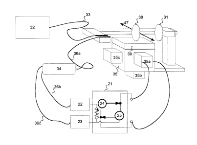
[0050] The primary embodiment of the invention is shown in Figure 5, the NC
circuit 21 is
used for obtaining automated alignment of a component 30, in the form of an
optical component,
to a light source 32. The light source 32, is optically coupled to a first
optical fibre 33, providing
light to the component 30. Light passes through the component 30 and is
reflected from off a
stationary mirror 31, and passes back through the same component and
illuminates a second
other optical fibre 36a. Both optical fibres 33 and 36a are fixedly mounted to
the mirror 31 and
an component positioning stage 35. The optical component 30 is coupled to a
single axis
moveable platform 39 as a moveable part of the stage 35.
[0051] Light from the second other optical fibre 36a is optically coupled to a
power sputter 34,
with each of the power sputter 34 output ports, 36b and 36c, optically coupled
to a
photodetector, 22 and 23. Photodetectors, 22 arid 23 are coupled to the NC 21
input ports. The
two NC 21 output ports are coupled to a DC motor as part 35a of the motorized
component
positioning stage 35. Only one axis 35a uses a motorized linear actuator
mechanism, comprising
a DC motor coupled to lead screw assembly as the moveable platform 39
actuation mechanism
35a. The NC output port corresponding to the first complementary output signal
is coupled to a
first terminal of the linear actuator 35a, and the NC output port
corresponding to the second
complementary output signal is coupled to a second terminal of the linear
actuator 35a.
[0052] The second 35b and third axes 35c of the component positioning stage
35, optical
fibres, and the mirror, are aligned in such manner that automated movement of
the component
parallel to the first axis 35a, results in an optical intensity profile having
a high optical loss
detected towards extremes of the component translation boundaries and having a
lower loss
closer to the component position of optimal alignment.
13
CA 02383318 2002-04-25
Patent
134-O1 CA(2)
[0053] In use, the NC controller coupled to the DC motor 35a, makes the DC
motor 35a turn in
both directions in response to the NC complementary output signal. This
results in an oscillatory
motion of the component 30 coupled to the platform 39; starting motion at an
initial base
frequency, in response to output signal times T l and T2. Of course the signal
times are
dependent upon the integrated resistance of the photodetectors 22 and 23
during dynamic
movement 47 of the component.
[0054] A higher optical power illuminating the photodetectors results in a
lower resistance on
the photodetectors and hence a smaller displacement of the component 30, as
shown in Figure
4c. A lower optical power illuminating the photodetectors results in a higher
resistance on the
photodetectors and hence a larger displacement of the component.
[0055] The NC causes asymmetric displacement 47 of the component in a
direction towards a
lower insertion loss through optimization for a balanced input resistance and
hence lower optical
loss. Through these oscillations the component is aligned to the optical
signal such that it
oscillates about the point of optimal alignment, with a displacement
proportional to the total
detected light intensity. At this point if the intensity of the optical source
is increased, or if the
resistance of the base frequency resistor 19 is decreased, then a point of
optimal alignment is
reached where the optical loss is at a minimum. In dependence upon the
resistance on the NC
input ports, this point of optimum alignment may corresponds to the lockup
frequency.
[0056] In Figure 6, a secondary embodiment of the invention is shown. In this
case, the same
component 30 positionable in a single axis 35a using a same three axis
positioner 35 as was
demonstrated in Figure 5. A light source 32 is optically coupled into a first
fiber 33, providing
light to the component 30. Light passes through the component and is reflected
from a mirror 31
and passes back through the component and illuminates a second other optical
fiber 36a. Light
from the second optical fiber 36a, optically couples into a photodetector 70.
The photodetector
70 output port is coupled to a controllable gain amplifier circuit (CGA) 71,
with the output port
of the CGA coupled to an optical coupling source photodiode (OCS) 73. The OCS
73 is
optically coupled via an optically communicative 48 environment 49 to a pair
of optical coupler
detector, OCD1 75 and OCD2 76. OCDI 75 and OCD2 76 couple into the NC 21 input
ports of
Nu1 and Nu2. The optically communicative environment permits exchange of
optical alignment
14
CA 02383318 2002-04-25
134-O1 CA(2) Patent
signal data between a detected and amplified optical signal and NC optically
coupled thereto.
The CGA circuit is designed to generate a predetermined voltage output on the
CGA output port
in dependence upon received photocurrent. The voltage output provided to the
OCS is either
logarithmic, linear; AC coupled, or of some calibrated relationship in
dependence upon received
photocurrent from the photodetector.
[0057] In use the alignment system shown in Figure 6 behaves almost
identically to that shown
in Figure 5. However, in this case a variable gain control port 72 is provided
as part of the CGA
circuit 71. This obviated the need for increasing the optical power of the
light source 32 during
execution of the alignment method, when attempting to reach the lockup
frequency. Increasing
the gain 72 on the CGA 71 causes the base frequency of the neural controller
to increase since
the emitted light intensity 48 of OCS 73 increases and as a result decreases
the resistance of
OCD 1 75 and OCD2 76.
[0058] Initially a lower base frequency is desired and so the gain of the CGA
circuit 71 is set
low as the alignment method begins to execute, thereby initially allowing for
a larger bi-
directional optical component displacement 47. Photodetectors, OCD 1 75 and
OCD2 76 are
responsive to variations in optical power of OCS 73 as the optical power
varies on the
photodetector 70. Coupled optical power illuminating PDLS I 70 with the
movement of the
component, resulting in the intensity of OCS 73 to vary, in relation to the
optical power
variations detected on the photodetector 70, after amplification by the CGA
71. Increasing the
gain 72 on the CGA 71 causes the base frequency to increase until such a point
is reached where
the base frequency causes the system to reach the lockup frequency. The
actuator and positioning
stage mechanically integrate the neural controller complementary output signal
through the
response time of various components making up the actuator, such as the DC
motor, lead screw
assembly, actuator moveable stage and optical component. The active LO of the
complementary
output signal is varying fast enough that the first complementary output
signal is not of enough
time duration to displace the actuator in a direction before the second
complementary output
signal causes displacement of the actuator in the other direction.
[0059] Optically coupling of PDLS 1 70 in this manner to the neural controller
circuit 21 offers
the benefit of varying the gain 72 on the CGA circuit 71 to facilitate varying
of the base
t5
CA 02383318 2002-04-25
Patent
134-O1 CA(2)
frequency, thereby increasing or decreasing the component bi-directional
displacement in
response to NC complementary output signal. It also allows for coupling of
multiple NCs to a
same OCS 73 such that an optical component can be disposed between the OCS and
coupling
detectors for modifying portions of the light emitted from the OCS.
[0060] Figure 7 shows the optical coupling between the CGA circuit 71, OCS 73,
and two NCs
83 and 84. Each of the NC have two optical coupler photodetectors, OCD I 75
and OCD2 76
coupled thereto. In a first coupling orientation 81 the anode of the
photodetector 75 is coupled to
the anode of the photodetector 76, with cathodes both coupled to a first NC
83. In a second
coupling orientation 82 the cathode of the photodetector 75 is coupled to the
cathode of the
photodetector 76, with anodes coupled to a second NC 84. Either coupling
configuration works
for purposes of optically coupling the optical alignment signal to the NCs.
[0061] This arrangement allows for two neural controller circuits 83 and 84,
to read from the
same photodetector 70 without mutually interfering. Coupling of the neural
controllers in such a
manner to a common detector allows for simultaneous execution of the alignment
methods
within both neural controller circuits. This allows the possibility for two
independent alignment
processes to execute within each neural controller. This type of controller
circuit arrangement
can be used in the aligning of the component in two axes simultaneously to the
optical signal.
[0062] In the embodiment of Figure 8, a single CGA circuit 71 is optically
coupled 48 using an
OCS 73 to each of the input ports of three NC circuits 21, within an optically
communicative
medium 49. Each NC 21 has its output ports coupled to each axis of a motorized
three-axis
component positioning mechanism 94. An optical stage controller (OSC) 91,
comprises three
NC circuits 21, with each NC circuit having a provision for optically coupling
an OCS 73
thereto. An optical element 87 is disposed between the light emitted 48 from
the OCS, and one
of the coupling photodetectors 75. The optical element 87 changes the
properties of the light 480
that interact with the optical element 87. As a result the light intensity
seen by OCD I as part of
the third NC circuit will be altered. If this optical element is an attenuator
then the transmitted
480 light intensity will be decreased, if it is a spectral filtering element,
then the OCD 1, as part
of the third NC, will be illuminated by the spectrally filtered portion of the
light. This allows for
filtering or attenuating of the light incident into a portion of this NC.
Thereby offering an optical
16
CA 02383318 2002-04-25
134-O1 CA(2) Patent
method for optically tuning the base frequency in response to the filtered or
attenuated light.
Advantageously, through adding of active and passive optical elements,
additional optical
processing on the optically coupled alignment signal can take place during
alignment of a
plurality of components to the optical signal.
[0063] The embodiment of Figure 9, shows an alignment system wherein a light
source 100
transmits light through a first component 101 via second component 102 into a
photodetector
103. Each of the components is coupled to a multi axis, moveable portion 104,
of the three-axis
motorized component positioning mechanism 94. Each of the two OSC 91 output
ports are
coupled to each of the three-axis motorized component positioning mechanism 94
motorized
axes. Light received by the photodetector 103 is coupled to the CGA circuit
71. The CGA OCS
is optically coupled to each of the two OSCs 91. through the optically
communicative medium
49.
[0064] The alignment method is initiated on both components 101 and 102, in
three axes, in
response to the light source 100 illuminating the photodetector 103. Up to six
alignment
processes execute within the optically coupled NCs. Both components are
aligned in three axes
in such a manner that after alignment an obtainable maximum amount of light
from the source
100 is illuminating the photodetector 103.
[0065] In the embodiment shown in Figure 10, a light source 100 is incident on
an optical
system, illuminating two components, 114, 115, and two detectors 11'? and 113.
The
photodetector 112 is coupled to a first CGA circuit 71 and the other
photodetector 113 is coupled
to a second CGA circuit 71. An output signal from the first CGA is coupled to
an OCS 1 16,
having a first predetermined spectral characteristic; an output signal from
the second CGA is
coupled to an OCS 117, having a second predetermined spectral characteristic.
Light from the
first OCS 116 emits light with a first wavelength 48. Light from the second
OCS 117 emits light
with a second wavelength 482. Light from both OCSs falls on either one of the
OSCs optically
coupled to both OCSs. Each of the OSC 91 output ports is coupled to an
actuator on each axis of
the three-axis motorized component positioning mechanism 94.
[0066] The alignment method executes within each of the NC within the OSC 91,
for the
automated positioning of the two components, in three axes, in response to the
light source
17
CA 02383318 2002-04-25
134-O1 CA(2) Patent
illuminating the two photodetectors. Each of the gain profiles within the CGA
circuits is variable
and as such is experimentally determined to offer optimal alignment. The
portion of the optical
coupling between each OCS and each OSC is also variable and experimentally
determined. In
some cases it may be advantageous to provide an increased optical signal from
one of the OCSs.
[0(167] In the embodiment shown in Figure 11, a light source 100 is incident
on an alignment
system. Wherein light output from the source 100, propagates through a
plurality of optical
components 122, 123, and illuminates a quadrant detector 126, having
photodetector elements
126a, 126b, 126c, 126d arranged in a predetermined manner therein. Each of the
photodetector
elements couples to one of a plurality of CGA circuits, 71 a, 71 b, 71 c, 71 d
respectively, for
further coupling of each CGA output to an OSC. Each OSC is optically coupled
to an OSC. Each
OSC is coupled to a motorized multi axis component positioning mechanism 94b,
94a. Optical
elementsl24, 125, and 87 are disposed within the optically communicative
medium 49 in order
to interact with the light emitted from each of the OCSs. These optical
elements are optical
elements such as filters and attenuators. These optical elements can take the
form of pigtailed
fibre optic components, such as those used in telecommunication. Within each
of the OSCs, 91,
the alignment method executes on the components 122 and 123 independence upon
the optical
power detected by photodetector 126 propagating through the optical system.
[0068] In the case of an automated alignment system, it may be desirable to
have control over
which axes of the motorized component positioning mechanism 94 are currently
being controller
by the NC for execution of the alignment method. It may not always be
preferable to execute the
alignment method on all components simultaneously, but rather move each of the
components
sequentially, and to move each of the axes within a motorized component
positioning mechanism
individually, with one process following another.
[0069] As is shown in Figure 12, each controller circuit, 210 and 135, has an
enable port 130
The enable port 130 is used for enabling or disabling the complementary output
signals for each
neural controller circuit. The enable port accepts enable signals at either a
HI level or at a LO
level. Where, an active LO level enables the neural controller circuit output
signals. Output ports
from NC 210 are coupled to a configurable drive amplifier circuit (CDA) 138.
1g
CA 02383318 2002-04-25
134-O1 CA(2) Patent
[0070] A sequential neural controller circuit (SNC) 135 comprises a ring
architecture of a
plurality of neurons. Each output port from one of the neurons couples to an
input port of another
neuron, in a ring architecture as shown in 135. In this manner, four output
signal, each having a
predetermined time duration, are output from four output ports as part of the
SNC. Into input
ports of the SNC, four optical coupling detectors are coupled thereto. Each of
the photodetectors
138 is in parallel with a variable resistor 137 for varying the resistance
applied to each of the NC
input ports. Photodetectors 138, and optical coupling detectors 75 and 76 are
within one of the
two optically communicative mediums 49. Each medium 49 receiving a portion of
the optical
alignment signal from an at least one OCS optically coupled thereto. Luring
sequential executing
of the alignment method, at least two different axes are controlled in
sequence. For instance if
the X and Y axes are being sequentially aligned, then the component will move
in a +X,
direction, then -Y, -X, +Y, +X, for example, where the sequential alignment
method repeats
until disabled 130, or until it reaches the lockup frequency.
[0071] This control port 130 is used for enabling or disabling the operation
of the alignment
method executing within NC circuits. This control port 130 is typically
coupled to another neural
controller circuit. An active LO level applied to the control port 130 enables
execution of the
alignment method within the neural controller, and an active HI level applied
to the control port
130 of the neural controller circuit causes the execution of the alignment
method to stop.
Coupling of this control port to another NC 129, allows the other NC 129 to
enable the execution
of the alignment method within the controlled NC 210 for a predetermined
amount of time in
dependence upon the output signal time from this neural controller circuit
129. Advantageously,
building a hierarchy of neural controller circuits, where enables are used on
some of the neural
controller circuits to enable timing of alignment method processes, allows for
the creation of a
very dynamic automated component alignment system.
[0072] Depending upon the type of actuation mechanism used for the positioning
of the
component, the position of the component will either remain fixed for a
latching component
positioning mechanism. Many state of the art linear motor actuators mechanisms
comprise a
latching mechanism, where in latching mode, upon removing electrical power to
the actuator the
position of the actuator will remains approximately fixed.
19
CA 02383318 2002-04-25
Patent
134-O1 CA(2)
[0073] If a minimal optical intensity is provided on the OCS, then the
frequency of the
complementary NC output signals is quite low. When the NC is used in active
alignment
experiments, each displacement of the component, as well as reading of the
photodetectors, is
initiated in direct correlation with the transition in the NC output signals.
Therefore if an actuator
with a fast enough response time is used, then the NC will form a lock-in
detection system where
the displacement of the component at the frequency of the NC output signal
becomes the lock-in
frequency for the NC. Of course this frequency will vary as the point of
optimal alignment is
approached. The NC initiates the read of a photodetector after the transition
edge from a second
level to a first level and integrating the optical power during this time
until a transition back to a
second level. Direct optical feedback form the alignment system enables the
neural controller to
form a very specific type of integrating lock-in signal detection for each
controlled axis.
[0074] The effects of biasing mechanics are reduced through the use of the CDA
138. Within
the CDA a processor determines a predetermined amplification response, or
relationship.
between NC output signals and the actuator control signal. A relationship
between NC output
signal times and actuator displacement, for the actuator coupled to a single
axis, is determined,
such that for a constant output signal time the approximate change in detected
optical power as a
result of the bi-directional component displacement is approximately constant
for each direction
for an approximately constant frequency applied NC complementary output
signal.
[0075] In this calibration mode, for each axis, the processor within the CDA
is used to
dynamically measure the change in optical power in response to the NC output
signal applied to
each actuator for displacing the component in the actuated axis. The processor
processes the
optical power response of component and predetermines a control signal
provided to the
actuator, for a plurality of NC output signal frequencies. This calibrated
relationship provides for
a NC complementary output signal to actuator control signal in such a manner
that optical
alignment system biasing mechanics for a given axis are minimized.
[0076] Minimizing alignment system unbalanced mechanical biasing in a
plurality of axes
results in an automated alignment system which has a high potential for fast
alignment times.
Since the predetermined amplification response is known for each axis, each of
the components
can be oscillated at higher frequencies because of known calibrated response
curves, which when
CA 02383318 2002-04-25
134-Ol CA(2) Patent
used for dynamically positioning the component result in an approximately bias
free response
dynamic response.
[0077] In some cases multiple CGAs, one for each axis, may have to be used in
order to obtain
the highest possible alignment speeds. The CGA response can be varied to
specifically respond
to unique control signal requirements for each axis. Advantageously, after
calibration and in use,
during aligning of components using a parallel or sequential alignment
processes, the gain profile
within each CGA is varied in such a manner as to facilitate the fastest
alignment times. The type
of amplification within the CGA and the calibrated response within the CDA are
both controlled
to obtain fastest alignment times.
[0078] Also within the calibration mode, the lockup frequency for each of the
automated
component axes is measured, for each of the actuators automating component
position in that
axis, thereby resulting in known lockup frequencies for each of the automated
axes within the
system to be grouped in dependence upon their lockup frequency. In this
manner, a CGA is
provided for each group such that by varying an input signal to the control
port of the CGA
makes all the automated axes grouped within this group, to lockup when the
frequency of the NC
output signals frequency is within the frequency band of the group. To
facilitate this coupling of
similar response axes within the group, optical fibres can be used as the
optically communicative
medium in order to optically link OSCs, SOSCs and CGAs.
[0079] Continuous execution of the alignment. method within the OSCs coupled
to actuators
and components in an optical alignment system, results in a potential
reduction in the effect of
external vibrations on the optical set-up during the active aligning. When the
alignment system is
aligned, with the components in optimal position, the alignment method is
still executing. If a
low frequency vibration occurs while al component is positioned in a position
of optimal
alignment the alignment method will compensate for the vibration by re-
converging the
components back to a position of optimal alignment. The faster the frequency
response of the
component positioning mechanism, the faster the component can be positioned
and the higher
the frequency of external vibrations that the alignment system can withstand.
A voice coil
actuating mechanism for the component is an alternate method of positioning of
the component
because the actuator satisfies the main criteria of having the capacity for
high frequency
21
CA 02383318 2002-04-25
l34-01 CA(2) Patent
operation. On average voice coils, such as the ones used in speakers, have a
frequency response
up to around 20kHz. Coupling this form of actuator mechanism to an component
allows for the
greatest range of operating frequencies, large displacement, providing the
fastest form of
.actuation for the component as well as allowing for a light and compact
component actuation
'mechanism. Many other embodiments of a voice coil actuator maybe envisioned
for this
;purpose, as well as using more than one voice coil actuator per axis.
However, in order to
maximize the effectiveness of voice coil actuators in high speed alignment
systems, coupling of
bulky positioning stages to the voice coil actuator is not desirable. Using
multi axis linear
bearing stages as well as flexure stages decreases the potential top speed
with which the voice
coil actuator can operate.
[0480] Reference is made to this circuit because of the simplicity involved in
using and
constructing such a control circuit, as well as the circuit lending itself to
this type of application.
Other controller circuits, or other software and hardware representations
thereof, may be
envisioned without departing from the scope or simplicity of this invention.
[0081] The above system is described for component alignment in general, but
it particularly
advantageous when applied to alignment of optical components.
[0082] Numerous other embodiments are envisaged without departing from the
spirit or scope
of the invention.
22