Note: Descriptions are shown in the official language in which they were submitted.
CA 02383394 2002-04-25
System and Method For Reducing Power Consumption By A Liquid Crystal Display
FIELD OF THE INVENTION
This invention relates generally to liquid crystal displays (LCDs). More
specifically, the
invention provides a system and method for reducing power consumption by an
LCD. This
invention is particularly well-suited for use in Personal Digital Assistants,
cellular telephones,
and wireless two-way email communication devices (collectively referred to
herein as "mobile
communication devices").
BACKGROUND OF THE INVENTION
Power conservation is an important design criterion for many devices that
utilize an LCD,
such as mobile communication devices. It is often important, therefore, to
minimize the power
consumed by an LCD. This goal is often accomplished by reducing the frame
frequency of the
I:.CD, which is proportionate to the LCD's power consumption.
Fig. 1 is a graph 10 that illustrates the power consumption of a typical LCD
as a function
of its frame frequency. In order to minimize power consumption while avoiding
the perception
of a flickering image on the LCD, the frame frequency is commonly set around
75 Hz. A lower
frame frequency will, however, still provide a virtually flicker-free display
in most
environments. For instance, a frame frequency of 68 Hz provides a display with
very little
clicker, and reduces the current consumption by approximately 70 ~.A, as shown
in Fig. 1.
Fig. 2 is a table 20 that shows the battery life of a typical mobile
communication device
as a function of its LCD current. As illustrated in this table 20 and also in
Fig. 1, if the average
1
CA 02383394 2002-04-25
I:.CD current is reduced to 0.7 mA by lowering the frame frequency of the LCD,
then the battery
life may be extended by approximately 2 days.
Fig. 3 is a block diagram of a typical system 30 for reducing the frame
frequency of an
LCD 36 during periods of inactivity. The system 30 includes a processing
device 32, an LCD
controller 34, and the LCD 36. The processing device 32 generates a clock
signal 38 that is
<;oupled as an input to a display timing circuit generator 40 in the LCD
controller 34. The
display timing circuit generator 40 controls the frame frequency of the LCD 36
by generating a
t ming output 39 based on the clock signal input 38. The timing output 39 is
coupled to an LCD
driver 44 which generates an analog drive voltage 37 for the LCD 36 using the
timing output 39
Gong with digital data 33 received from the processing device 32 and stored in
a memory device
42. The processing device 32 may, therefore, reduce the frame frequency of the
LCD 36 by
reconfiguring the clock signal 38.
Operationally, the processing device 32 conserves power by reducing the frame
iTequency of the LCD 36 when the system 30 has been inactive for a pre-
determined period of
time. For instance, if the system 30 is in a mobile communication device, then
the processing
device 32 may monitor user interaction, and reduce the frame frequency if the
user has not
interacted with the device for a selected amount of time. Once user activity
is detected by the
processing device 32, the frame frequency of the LCD 36 is returned to a level
suitable for
comfortable viewing. Even during periods in which the frame frequency is
reduced, however,
this system 30 requires the processing device 32 to continue generating the
clock signal 38, thus
consuming power and reducing battery life.
2
CA 02383394 2002-04-25
SUMMARY
A system for reducing power consumption by a liquid crystal display (LCD) is
provided.
I~ne embodiment includes a processing device, an LCD controller and a
switching device. The
processing device is configured to generate a digital output having a first
state and a second state.
'the LCD controller is coupled to the LCD and has a display clock input,
wherein the frequency
of the display clock input controls the frame frequency of the LCD. The
switching device has a
first input coupled to a first clock signal and a second input coupled to a
second clock signal, and
has a control input coupled to the digital output of the processing device.
The first clock signal
Izas a first frequency and the second clock signal has a second frequency. The
switching device
couples the first clock signal to the display clock input to the LCD
controller when the digital
output of the processing device is in the first state and couples the second
clock signal to the
display clock input to the LCD controller when the digital output of the
processing device is in
the second state.
Another embodiment includes a processing device and an LCD controller. The
processing device is configured to detect a triggering event in the mobile
communication device
and to generate an event trigger signal. The LCD controller, which includes a
switching device
and a timer, is coupled to the processing device. The switching device has a
control input, a first
:input coupled to a first clock signal of a first frequency, and a second
input coupled to a second
clock signal of a second frequency. The timer is coupled to the event trigger
signal and the
control input of the switching device. The timer generates a control signal on
the control input to
the switching device to select the first input to the switching device as a
display clock output
from the switching device when the event trigger signal indicates the
occurrence of the triggering
3
CA 02383394 2002-04-25
event. In addition, the control signal generated by the timer selects the
second input to the
switching device as the display clock output from the switching device if the
triggering event has
not been detected for a pre-determined time interval. The LCD controller
controls the frame
frequency of the LCD as a function of the display clock output from the
switching device.
BRIEF DESCRIPTION OF THE DRAWINGS
Fig. 1 is a graph that illustrates the power consumption of a typical LCD as a
function of
i.ts frame frequency;
Fig. 2 is a table that shows the battery life of a typical mobile
communication device as a
function of its LCD current;
Fig. 3 is a block diagram of a typical system for reducing the frame frequency
of an LCD
during periods of inactivity;
Fig. 4 is a block diagram of an exemplary LCD power conservation system;
Fig. 5 is block diagram of another exemplary LCD power conservation system;
Fig. 6a shows a typical LCD display in a mobile communication device during
normal
operation;
Fig. 6b shows the typical LCD display of Fig. 6a in an exemplary reduced pixel
mode of
operation; and
Fig. 7 is a flow diagram illustrating an exemplary method for implementing
dynamic
:frame frequency adjustment and a reduced pixel mode for an LCD.
DETAILED DESCRIPTION
4
CA 02383394 2002-04-25
Referring now to the remaining drawing figures, Fig. 4 is a block diagram of
an
exemplary LCD power conservation system 50. The LCD power conservation system
50
includes a processing device 52, an LCD controller 54 and an LCD 56. In
addition, the system
:i0 includes a switching device 58, a divider 60, and an external oscillator
62. Operationally, the
processing device 52 controls the frame frequency of the LCD 56 by using the
switching device
a8 to select between a first clock signal 63 generated by the external
oscillator 62 and a slower,
second clock signal 67 generated by the divider 60.
The processing device 52 generates a digital output 66 that is coupled as a
control input
i:o the switching device 58. In addition, the processing device 52 is coupled
to the LCD
controller 54 by a data line 70 and a control line 72 that transmit display
data and commands
from the processing device 52 to the LCD controller 54. The processing device
52 may, for
example, be a central processing unit (CPU), a digital signal processor (DSP),
or some other type
of processor or dedicated logic circuitry. The switching device 58 may, for
example, be a
multiplexer, or may be some other type of switching component or circuitry.
The external oscillator 62 generates the first clock signal 6:S which is
coupled as one
input to the switching device 58 and is also coupled to the divider 60. The
divider 60 divides the
:first clock signal 63 by a pre-determined value (N), and generates a slower,
second clock signal
67, which is coupled as a second input to the switching device 58. The divider
60 may, for
example, be a divide-by-N counter, or rnay be some other type of circuit or
component capable
.of dividing the frequency of a signal by a pre-determined value (N). The
switching device 58
.also receives a control input 66 from the processing device 66, which
controls which of the first
or second clock signal inputs 63, 67 is coupled as a display clock signal 68
input to the LCD
5
CA 02383394 2002-04-25
controller 54. If a slower frame frequency ("alternate frame frequency") for
the LCD 56 is
desired, then the processing device 52 selects the slower, second clock signal
67 as the display
clock 68. Similarly, for a faster frame frequency ("primary frame frequency")
suitable for
comfortable viewing, the processing device 52 selects the first clock signal
63.
The LCD controller 54 in this embodiment 50 may be one of numerous
commercially
available LCD controllers known to those skilled in the art. A typical LCD
controller 54 may
include a display timing circuit generator 64, an LCD driver 65, and a memory
device 61. The
LCD controller 54 receives the data and control signals 70, 72 from the
processing device 52,
stores the digital data 70 to the memory device 61, and generates an analog
drive voltage 74 for
t:he LCD 56. The analog drive voltage 74 is generated by the LCD driver 65
using the digital
data 70 in the memory device 61 to be displayed on the LCD 56 along with a
timing output 75
generated by the display timing circuit generator 64. The timing output 75
from the display
timing circuit generator 64 controls the frame frequency of the LCD 56, and is
generated as a
function of the display clock signal 68 input to the display timing circuit
generator 64.
In operation, the frame frequency of the LCD 56 is decreased to the alternate
frame
frequency by selecting the slower clock signal 67 when a user is not likely to
be viewing the
1LCD 56. For instance, the alternate frame frequency may be selected if the
processing device 52
detects a period of inactivity, such as after a pre-determined timeout
interval expires without the
occurrence of any triggering events. The length of the timeout interval may be
based, for
example, on desired power savings and user perception. The timeout interval
should not,
however, be so short that the frame frequency will likely change as the device
user is still
actively viewing the LCD 56.
6
CA 02383394 2002-04-25
When the processing device 52 detects some triggering event, the frame
frequency is
increased to the primary frame frequency by selecting the faster clock signal
63. For instance, if
t:he system 50 is implemented in a mobile communication device, then the
triggering event may,
for example, be some activity on a user interface such as a keyboard, keypad,
thumb-wheel, or
stylus pad. Other types of triggering events may include, for example, the
receipt of an
electronic message by the mobile communication device, or placing the mobile
communication
device in an interface cradle.
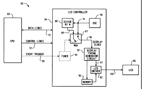
Fig. 5 is a block diagram of another exemplary LCD power conservation system
80. The
system 80 includes a processing device 82, an LCD controller 84 and an LCD 86.
The LCD
controller 84 includes an internal oscillator 90, a divider 88, a switching
device 87, a timer 94, a
display timing generator 92, an LCD driver 93, and a memory device 95. In this
exemplary
embodiment 80, the dynamic frame frequency adjustment described above is
incorporated into
the LCD controller 84.
Operationally, the switching device 87 internal to the LCD controller 84
selects between
a first clock signal 91 generated by the internal oscillator 90 and a slower,
second clock signal 89
;generated by the divider 88. The switching device 87 is controlled by a
control input from the
imer 94 and couples the selected clock signal 89 or 91 as the display clock
input 96 to the
display timing generator 92. The display timing generator 92 outpula a timing
signal 97 to the
LCD driver 93 which controls the frame frequency of the LCD 86 though an
analog drive
voltage 102.
The display clock signal 96 output from the switching device 87, and thus the
frame
frequency of the LCD 86, is controlled by the timer 94. The timer 94 monitors
an event txigger
7
CA 02383394 2002-04-25
signal 99 from the processing device 82 which indicates the occurrence of a
triggering event.
'When a triggering event is detected, the timer 94 resets and generates a
control signal to the
switching device 87, selecting the faster clock signal 91 from the internal
oscillator 90 as the
display clock 96, and thus selecting the primary frame frequency for the LCD
86. If a pre-
determined timeout interval expires before another triggering event is
detected by the timer 94,
then the timer 94 reduces the frame frequency of the LCD 86 to the alternate
frame frequency by
selecting the slower clock signal 89 as the display clock signal 96. The event
trigger signal 99
may, for example, be a hardware or software signal, or alternatively may be
the lack of activity
on control lines 72.
In addition, the timer 94 may place the LCD 86 in a reduced pixel mode by
generating a
reduced-pixel-mode-ON signal to the LCD controller 84 upon expiration of the
timeout interval
without the occurrence of a triggering event. In reduced pixel mode, portions
of the LCD 86 that
.are not needed when the mobile device user is not actively using the device
are automatically
turned off or "blanked". Thus, the user does not have to intervene in order
for the device to enter
this reduced pixel mode. Then, upon the occurrence of a triggering event, the
timer 94 generates
a reduced-pixel-mode-OFF signal to the LCD controller 84 to return the LCD 86
to normal
operation.
Fig. 6a shows a typical LCD display 110 in a mobile communication device
during
normal operation 112, wherein a number of application icons 116 are displayed
on the LCD.
Fig. 6b shows the typical LCD display 110 in an exemplary reduced pixel mode
114, wherein the
.application icons 116 have been blanked. The difference between the current
consumed by a
typical LCD during normal operation and a completely blanked LCD screen may
generally be
8
CA 02383394 2002-04-25
aground 150 N,A. Thus, the use of an automatic reduced pixel mode, either by
itself or in
combination with the alternate frame frequency, may significantly reduce power
consumption by
a mobile communication device during periods of inactivity. It should be
understood, however,
that the reduced pixel mode 114 in Fig. 6b is shown for illustrative purposes
only. In other
embodiments, placing the LCD in reduced pixel mode may cause different
portions of the
display to be blanked, or may cause the entire display to be blanked.
In one embodiment, the LCD controller 84 may include a memory device, such as
a
register set, that stores configurable parameters for the LCD conixoller 84.
The stored
parameters may, for example, set the timeout interval of the timer 94, the
clock frequency of the
internal oscillator 90, the division constant (N) of the divider 88, or other
device parameters. An
exemplary register set for configuring the LCD controller 84 device parameters
may be as
follows:
Register 1 - defines the number of lines to be blanked in reduced pixel mode;
Register 2 - defines the start line for reduced pixel mode;
Register 3 - defines the primary frame frequency;
Register 4 - defines the alternate frame frequency;
Register 5 - defines when to invoke the reduced pixel mode and/or the
alternate frame
frequency;
Register 6 - defines the timeout period; and
Register 7 - includes control bits (see Table 1 below).
'The control bits stored in the register set may, for example, be defined as
shown in Table 1.
9
CA 02383394 2002-04-25
Table 1
Bit Number Power-Up StateFunction
0 0 1 = on timeout invoke reduced pixel mode
0 = do not invoke reduced pixel mode on
timeout
1 0 1 = on timeout invoke alternate frame
frequency
0 = do not invoke alternate frame frequency
on timeout
2 0 1 = turn reduced pixel mode on now
0 = turn reduced pixel mode on only at
timeout
3 0 1 = invoke alternate frame frequency now
0 = invoke alternate frame frequency only
at timeout
4 X Reserved for future use.
X Reserved for future use.
6 X Reserved for future use.
7 X Reserved for future use.
5
In one alternative embodiment, the LCD controller 84 may include two timers 94
- one
timer to trigger the reduced pixel mode, and one timer to invoke the alternate
frame frequency.
In this embodiment, the device parameters may be configured to implement each
of these two
power-saving modes at different times. For instance, the reduced pixel mode
may be invoked
CA 02383394 2002-04-25
after a first period of inactivity, such as 10 minutes, and the alternate
frame frequency may be
implemented after a second period of inactivity, such as 15 minutes.
Fig. 7 is a flow diagram 120 illustrating an exemplary method for implementing
dynamic
frame frequency adjustment and a reduced pixel mode for an LCD. In step 122, a
triggering
t:vent is detected. Upon detection of the triggering event, the frame
frequency of the LCD is set
t:o its primary frame frequency (step 124) and the reduced pixel mode is
turned off (step 126),
putting the LCD in its normal mode of operation. Then, a timeout countdown
begins at step 128
;end is reset at each occurrence of a triggering event (step 130). If the
timeout countdown
continues without being reset for a pre-determined timeout interval (step
132), then the reduced
pixel mode is invoked at step 134 and the frame frequency is set to the
alternate frame frequency
at step 136. The LCD remains in reduced pixel mode and continues to operate
with the alternate
.frame frequency until a triggering event is detected (step 138), causing the
method to repeat at
step 122.
This written description uses examples to disclose the invention, including
the best mode,
and also to enable any person skilled in the art to make and use the
invention. The patentable
scope of the invention is defined by the claims, and may include other
examples that occur to
those skilled in the art.
11