Note: Descriptions are shown in the official language in which they were submitted.
CA 02383898 2008-03-07
1
Signal Switching
The present invention is concerned with the switching of signals, for
example for routing signals to an output from one of two alternative feeds and
switching to the other feed in the event of signal disturbance of
interruption. It finds
particular application in the switching of digital television signals, but may
also be
applied to other types of signal.
Russo (Russo E: 'Implementation of a Space Diversity System for KaBand
Satellite Communications' Proceedings of the International Conference on
Communications (ICC), IEEE, vol. 3, 23 May 1993 (1993-05-23), pages 1468-1474)
describes a system for switching between two alternative data streams for each
stream, with a buffer or elastic memory and means for synchronising the two.
Errors are detected at the input and trigger switching from one memory to the
other. A clock for memory readout is synchronised to the incoming signal.
A problem that can arise with such systems is that, although the buffer
contains uncorrupted data and allows a period of grace during which to take
remedial action, the same is not true of the readout clock, The present
invention
aims to alleviate this problem.
The invention in its various aspects is defined in the claims.
Thus, the provision of the locally generated timing signals allows extra time
which permits switching to be performed in an orderly fashion, in terms of
buffer
synchronisation and selection of an appropriate time at which to switch, and
allows
switching to be avoided in cases of only minor disturbance of the incoming
signal.
Some embodiments of the invention will now be described, by way of
example, with reference to the accompanying drawings, in which:
Figure 1 is a block diagram of a switching device; and
Figure 2 is a flowchart illustrating the operation of part of Figure 1.
The version of the invention now to be described is a switching device for
digital signals, designed specifically for digital television signals of the
type used for
digital television broadcasting as defined in the European Committee for
Electrotechnical Standardisation (CENELEC) standard EN50083-9 dated June 1998.
However it should be borne in mind that the invention does not require that
the
signals are formatted in accordance with this standard, or, indeed, that they
be
television signals at all.
CA 02383898 2008-03-07
2
The standard envisages a packet structure consisting of 204 bytes (1 byte
= 8 bits), comprising a synchronisation byte (47h) followed by 187 data bytes
containing video data encoded in accordance with the so-called MPEG-2 standard
(ITU standard H.222) and 16 further bytes whose content is not prescribed but
may
typically contain error correction information using a Reed-Solomon code.
These 16-
bytes are optional, so that a 188-byte packet may be used instead. These
packets
may be generated at any desired data rate, so, in the interests of providing a
standardised interface, the standard envisages the reformatting of these data
into a
higher-rate data stream according to one of a number of defined formats. The
one
used in this example, called the Asynchronous Serial Interface (ASI), operates
at a
fixed bit rate (270 Mbit/s).
Conversion of the packets into ASI format involves translating each byte
into a 10-bit word using a look-up table. 512 10-bit words are allocated for
this
purpose (each byte has two possible translations - the one chosen being that
which
minimises the disparity of the transmitted signal - i.e. minimises the
difference
between the number of "1" bits and the number of "0" bits transmitted).
Additional
10-bit words are allocated for special purposes; in particular one is
allocated as a
synchronisation word. The translated words (referred to as data words, it
being
understood that this term includes the translated packet synchronisation bytes
as
well as the translated MPEG-2 data bytes) are presented to a parallel-to-
serial
converter and output in serial form at 270 Mbit/s. Gaps between data words are
filled with synchronisation words so that the number of synchronisation words
between each pair of consecutive data words is substantially constant. Of
course, it
can only be exactly constant if the incoming byte rate is an exact sub-
multiple of the
outgoing byte rate of 27 Mbyte/s.
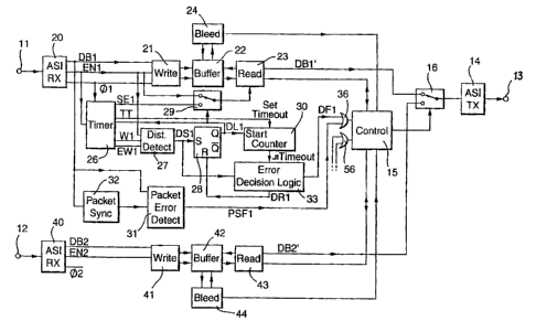
Figure 1 is a block diagram of a switching device. It has two inputs 11, 12
which receive respectively primary and secondary feeds of video in ASI format
as
described above. Its function is to convey one of the feeds to an output 13,
again
in ASI format, and, in the event of disturbance or interruption of that feed,
to switch
over to the other feed. The two feeds are referred to as primary and secondary
in
the expectation that the device always defaults to conveying the primary feed,
and,
after switching to the secondary feed, reverts to the primary feed when the
disturbance or interruption has cleared. However it is equally possible to
regard the
feeds as being of equal status, in which case reversion is unnecessary. It is
CA 02383898 2008-03-07
3
expected that the two feeds have the same information content (i.e. the same
pictures) and that they are supplied by telecommunications links passing over
different routes (to minimise the risk of both feeds being disturbed or
interrupted)
though neither of these factors is material to the technical functioning of
the
switching device per se. Note however that the switching device is designed to
accommodate the possibility that the two feeds originate from separate ASI
coders
which, whilst operating at the same data rate, may not necessarily be in
synchronisation - i.e. the number of synchronisation bytes between a given
pair of
data bytes may not necessarily be the same in the two feeds.
The primary input 11 is served by an ASI receiver 20. This is of
conventional construction (for example as available from Cypress Semiconductor
Corporation, as also is the ASI transmitter referred to below). It receives
the ASI
signal and serves to recover bit and (using the received synchronising words)
byte
synchronisation, and decodes the received 10-bit words. Each time it receives
a 10-
bit serial word which corresponds to an 8-bit data byte it outputs the byte
13131 in
parallel format. A second output delivers an 'enable' signal EN1 whenever such
a
word is received. Thirdly, it outputs a byte clock 4)1.1.
The recovered bytes 13131 are now restored to the original 204 (or 188) -
byte sequence. These are fed via write circuitry 21 to a first-in-first-out
(FIFO)
buffer 22. Whenever the write circuitry receives the enable signal EN 1 it
writes the
received byte into the buffer 22. Under normal operation, the bytes are read
from
the buffer by readout circuitry 23, under control of the same enable signal EN
1.
Upon start-up, the read circuitry does not begin reading until the buffer is
half-full:
once reading commences, the buffer fullness remains constant. Typically, the
buffer
will be of a size sufficient to accommodate 20 packets. Apart of course from
the
buffer delay, the sequence of data bytes 13131' read from the buffer is
identical to the
sequence 13131 input to it. This sequence is supplied to an ASI transmitter 14
which
recodes the signal into ASI format before delivering it to the output 13.
The second input 12 is fed via an ASI receiver 40 and write circuitry 41 to a
buffer 42 in exactly the same manner as described above. Read circuitry 43 are
not
active in this mode, and data bytes are not read out. The buffer is maintained
at
approximately half-occupancy by bleed circuitry 44 which, whenever the buffer
occupancy exceeds the half-way point, deletes the oldest complete 204-byte (or
188 byte) packet from the buffer.
CA 02383898 2008-03-07
4
Before describing the response of the device to disturbances to the
incoming signal, further circuitry to make this possible will be introduced. A
timing
device 26 is provided which receives the enable signals EN1 and the byte clock
4)1.
By counting the byte intervals between each occurrence of the enable signal it
calculates the actual data rate (i.e. the number of enables per second or the
average
period between enables: note that is general this is not a whole number of
byte
periods). It uses this information to calculate the expected time of
occurrence of the
next enable signal and produces three byte-synchronous signals: a synthesised
enable signal SE1 occurring at this expected time, a window signal W1 active
during
a period of five byte periods' duration centred on this expected time, and an
extended window signal EW1, active during the expected time of occurrence, two
byte-periods before and seven byte periods after. It will be seen that, by
monitoring
for disturbances at the input to the buffer, the delay occasioned by the
buffer 22
allows, in the event of disturbance or interruption of the signal on the input
11, a
period of grace during which to take remedial action, since uncorrupted data
is still
present in the buffer - i.e. this provides a fault look-ahead technique). The
same
however cannot be said of the enable signal EN 1 which is used to control
buffer
readout. Thus the response of the device to disturbance falls into two
distinct
phases.
(a) initial recognition of disturbances to the signal and substitution into
the
buffer readout process of the locally generated enable signal SE1 instead of
the
incoming enable signal EN 1; and
(b) recognition of serious disturbance and feeding the ASI transmitter 14
from the secondary feed, via the buffer 42.
In this embodiment, the criterion for initial recognition of disturbances is
that
the arrival of valid bytes as indicated by the enable EN 1 does not correspond
(within
a margin of error) to that expected. The detection is performed by a detector
27
which produces an output signal DS1 in the event that either of two conditions
is
satisfied:
(i) that EN 1 occurs outside the 5-byte window defined by W1 twice in
succession (i.e. without the intervening occurrence of EN1 within the window)
(ii) that EN1 fails to occur during the 10-byte window defined by EW1.
The signal DS1 sets a latch 28 which, when set, produces an output signal
DL1 which triggers a changeover switch 29 so that the synthesised enable
signal
CA 02383898 2008-03-07
SE1 is fed to the readout circuitry 23 instead of the received enable signal
EN1. The
signal DL1 is also fed back to the timing device 26 where it suppresses any
further
updating of the calculated data rate on the basis of the enable signals EN)
currently
being received. Once this enable signal switchover has occurred, the signal
DS1 is
5 monitored for further disturbances. A dynamic timeout mechanism is employed,
with a timeout period proportional to the packet rate of the current feed.
This
period TT is calculated (as described below) in the timing unit 26. When the
latch
28 is set, a counter 30 is started - i.e. it is loaded with a value
corresponding to the
period TT and begins to count down. In the event that no further disturbance
signals DS1 are received during the timeout period, a signal DR1 is generated
by
error decision logic 33, which resets the latch 28 and thus switches the
switch 29
back to its original position. If however, at least one further disturbance
has been
detected, a signal DF1 is produced which initiates a process of switching over
from
the primary feed to the secondary feed.
The object of the dynamic timeout control is to ensure that the timeout
period corresponds to a fixed number of packets, irrespective of the actual
data rate.
This ensures that the incoming signals are monitored over an adequate period,
whilst
ensuring that the feed switchover process can be completed before any serious
disturbance has reached the output of the buffer 42.
Worked example of dynamic timeout period:
Incoming bit rate = 26.181818Mbit/s in 204 byte packets
Incoming byte rate = 3.27272725 Mbytes/s
Incoming packet rate = 16042.78 packet/s (204 byte packets)
Packet duration = 62.3333 ps
Buffer capacity = 20 packets and thus 10 packets for mid point operation.
Since loss of signal takes 4 lost packets this would allow buffer to drop
nearly half
its normal operating level and this is deemed acceptable for dynamic timeout
period.
Dynamic timeout period = 4 x Packet Duration = 249.3333 s
CA 02383898 2008-03-07
6
The timer 26 thus, having ascertained the byte rate (as mentioned earlier),
calculates the necessary count TT of the counter 30 to correspond to the
required
timeout period.
Additionally, a packet alignment detector 31 monitors the received bytes
DB1. Following acquisition of packet synchronisation by a packet
synchronisation
unit 32, the detector 31 detects failure of the packet sync byte to appear on
four
consecutive packets and if so produces an output PSF1 to force initiation of
switchover (irrespective on whether enable switchover has already occurred).
Note that the byte clock 4) is used to clock data in to the FIFO 21 and to
drive the discontinuity block 27, packet sync block 32, error detect block 31
and the
data rate calculation part of the timing block 26. Not all of these
connections are
shown in Figure 1.
The feed switching process is performed by a control unit 15 in the form of
a stored program - controlled microprocessor. This process must be performed
in
an orderly fashion in order to ensure that switching occurs at a packet
boundary,
and is illustrated in the flowchart of Figure 2.
In step 101, the control unit 15 checks whether the buffer 42 is in the
process of being bled, in which case it waits until a packet boundary is
located as
indicated in step 102 .
Once the buffer 42 is aligned at a packet boundary, the bleed unit 44 is
locked (step 104) so that the buffer remains in readiness to output a complete
packet. In step 105, the control unit checks whether the primary channel
buffer
readout circuit 23 has reached the end of a packet, and if not, it waits until
it has.
Then at 106, it switches a changeover switch 16 so that the ASI transmitter 14
is
now fed from the secondary channel buffer readout circuit 43: the readout
circuit
43 is then enabled so that the last packet output from the primary feed
readout
circuit 23 is directly followed by a complete packet from the secondary feed
readout
circuit 43.
If desired, provision may be made for fault conditions other than those
described to initiate switching, for example an error detector (not shown)
could
monitor the parity of the 10-bit ASI words and/or error-check codes in the
last 16
bytes of a 204-byte packet and feed a fault signal to a further input of the
OR-gate
36 feeding the control unit 15.
CA 02383898 2008-03-07
7
Assuming that the two feeds are of equal status, the device remains
switched to the secondary input, until such time as a disturbance on the
secondary
feed may initiate a switchover in the opposite direction. It should be
understood
that the two paths through the device are identical, thus the buffer 22 has
bleed
circuitry 24 like the bleed circuitry 44, and the items numbered 26 to 36
associated
with the input 11 are duplicated for the lower input 12, though, in the
interests of
clarity, they are not shown in Figure 1. Items 13, 14, 15 and 16 are common to
both paths. If it is desired that the device should revert to the primary feed
once the
problem that gave rise to the switchover has cleared, this could of course be
arranged. For example, a detector could be provided to monitor the outputs of
the
detectors 27 and 31 and, in the event that no disturbances or errors[I occur
for a
certain period - perhaps an hour, to instruct the control unit 15 to switch
back. In
this case, the bleed circuitry 44 and the lower-path duplicates of items 26 to
36
could be omitted, although this is not preferred since this would involve a
loss of
security during the period that the secondary feed is in use.
Another refinement that could be introduced, if desired, is to monitor the
relative quality of the two feeds, and suppress any switching command if its
effect
would be to switch to a feed whose performance is actually worse than that
currently supplying the output.
The device of Figure 1 has been described as having two feeds; however the
principle can easily be applied to systems with three or more - switching from
one
feed to another in strict rotation, for example, or choosing the one with the
best
signal.
It will be observed that the arrangement described above with reference to
Figure 1, although it ensures a continuous stream of whole packets at the
input of
the ASI transmitter 14, does not guarantee continuity of packets at the moment
of
switchover of the switch 16. In other words, it is possible that packet
duplication or
packet loss may occur. This is considered to be acceptable in the case of MPEG
signals. If however, for any particular application, it is desired to avoid
this, it would
be possible, provided that the packets were labelled is some way, to provide
additional circuitry to examine the packets in the buffers and to adjust the
state of
fullness of the buffer 42 (or 22 when the secondary feed is in use) so as to
avoid
such duplication or loss.
CA 02383898 2008-03-07
8
Finally, the timing substitution technique described above could be used in
systems with a single feed and no feed-switching; in such a case, only items
11, 23,
14, 20 to 23 and 27 to 29 would be required.