Note: Descriptions are shown in the official language in which they were submitted.
CA 02384463 2002-03-08
WO 01/18860 PCT/US00/24847
IMPROVED APPARATUS AND METHODS
FOR INTEGRATED CIRCUIT PLANARIZATION
FIELD OF THE INVENTION
The present invention relates to semiconductor devices, including integrated
circuit
("IC") devices. More particularly, it relates to a methods and apparatus for
planarizing and/or embossing patterns onto surfaces of semiconductor devices
that
contain silica dielectric coatings, and particularly nanoporous silica
dielectric
coatings, as well as to semiconductor devices produced by these methods and
apparatus.
BACKGROUND OF THE INVENTION
Processes used for the fabrication of semiconductor devices almost invariably
produce surfaces which significantly deviate from a planar configuration. With
the
trend toward greater large scale integration, this problem is expected to
increase. For
instance, the production of integrated circuits typically requires multiple
layers to be
formed sequentially on a semiconductor substrate. Many of these layers are
patterned
by selective deposition or selective removal of particular regions of each
such layer.
It is well known that small deviations from the planar condition in underlying
layers
become more pronounced with the addition of multiple additional layers of
semiconductor and circuit features. Non-planar substrate surfaces can cause
many
problems that adversely impact the yield of finished products. For example,
variations in interlevel dielectric thickness can result in failure to open
vias, poor
adhesion to underlying materials, step coverage, undesirable bends or turns in
conductive metal layers, as well as "depth-of focus" problems for optical
lithography.
In order to effectively fabricate multiple layers of interconnects it has
become necessary to
globally planarize the surface of certain layers during the mufti-step
process. Planarizing
smoothes or levels the topography of microelectronic device layers in order to
properly
pattern the increasingly complex integrated circuits. IC features produced
using optical or
CA 02384463 2002-03-08
WO 01/18860 PCT/US00/24847
other lithographic techniques require regional and global dielectric
planarization where the
lithographic depth of focus is extremely limited, i.e., at 0.35 pm and below.
As used herein,
the term "local planarization" refers to a condition wherein the film is
planar or flat over a
distance of 0 to about 5 linear micrometers. "Regional planarization" refers
to a condition
wherein the film is planar or flat over a distance of about 5 to about 50
linear micrometers.
"Global planarization" refers to a condition wherein the film is planar or
flat over a distance
of about 50 to about 1000 linear micrometers. Without sufficient regional and
global
planarization, the lack of depth of focus will manifest itself as a limited
lithographic
processing window.
One previously employed method of planarization is the etch-back technique. In
that
process, a material, i.e., a planarizing material, is deposited on a surface
in a manner adapted
to form a surface relatively free of topography. If the device layer and the
overlying material
layer have approximately the same etch rate, etching proceeds through the
planarizing
material and into the device layer with the surface configuration of the
planarizing layer
being transferred to the device material surface. Although this technique has
been adequate
for some applications where a modest degree of planarity is required, present
planarizing
materials and present methods for depositing the planarizing material are
often inadequate to
furnish the necessary planar surface for demanding applications such as in
submicron device
fabrication.
The degree of planarization is defined as the difference between the depth of
the topography
on the device surface ht, and the vertical distance between a high point and a
low point on the
overlying material surface hd, divided by the depth of the topography on the
device surface
h~:
hip
The degree of planarization, in percent, is
2
CA 02384463 2002-03-08
WO 01/18860 PCT/US00/24847
h~_ ha x 100
Generally, for typical device configurations, planarization using the etch-
back technique has
not been better than approximately 55% as calculated by the method described
above for
features greater than 300 microns in width. The low degree planarization
achieved by this
technique is attributed to a lack of planarity in the planarizing material.
Thus, for elongated
gap-type features greater than 300 microns in width and 0.5 microns in depth,
the usefulness
of an etch-back technique has been limited.
U.S. Patent No. 5,736,424, incorporated herein by reference in its entirety,
describes a
method for planarizing surfaces of substrates, such as semiconductor
materials, by
adding a pressing step to an etch-back process. In this reference, an
optically flat
surface is impressed on a curable viscous polymer coating on the substrate
surface in
need of planarization, followed by polymerization of the coating. The polymer
is
selected to etch at the same rate as the surface in need of planarization, and
the
polymer coating is etched down to the substrate, which is planarized by the
process.
While an improved planarization is claimed, apparently by starting the etch-
back with
a flatter surface, an added process step and complexity is required. In
addition, this
reference fails to provide a solution for planarizing substrates coated with
nanoporous dielectric films, since by their nature, such low density films
cannot be
etched at the same rate as the underlying substrate.
Chemical mechanical polishing (CMP) is another known method that has been
effectively
used in the art to globally planarize the entire surface of dielectric layers.
According to this
method, a grainy chemical composition or slurry is applied to a polishing pad
and is used to
polish a surface until a desired degree of planarity is achieved. CMP can
rapidly remove
elevated topographical features without significantly thinning flat areas.
However, CMP
does require a high degree of process control to obtain the desired results.
3
CA 02384463 2002-03-08
WO 01/18860 PCT/US00/24847
Dielectric films formed of organic polymers, such as polyarylene ether and/or
fluorinated polyarylene ether polymers, have been planarized by applying CMP
to a
partially cured film, followed by a final curing, as described in co-owned
U.S. serial
number 09/023,415, filed on February 13, 1998, the disclosure of which is
incorporated by reference herein in its entirety. However, this reference
fails to
disclose how to planarize a silicon-based nanoporous dielectric material on
the
surface of a substrate.
Further, these previous methods are inadequate for providing localized
planarization on
different areas of a substrate surface, or for embossing other types of
topography onto
specific portions of a substrate surface. This is particularly important as
the move towards
ever larger integrated surface devices requires multiple planar surfaces,
vias, trenches and the
like, on disparate portions of a single substrate.
In addition, as IC feature sizes approach 0.25 pm and below, problems with
interconnect RC
delay, power consumption and signal cross-talk have become increasingly
difficult to
resolve. The integration of low dielectric constant materials for interlevel
dielectric (ILD)
and intermetal dielectric (IMD) applications, is helping to solve these
problems. One type of
such low dielectric constant materials are nanoporous films prepared from
silica, i.~, silicon-
based materials. When air, with a dielectric constant of 1, is introduced into
a suitable silica
material having a nanometer-scale pore structure, dielectric films with
relatively low
dielectric constants ("k"), g.~, 3.8 or less, can be prepared on substrates,
such as silicon
wafers, suitable for fabricating integrated circuits.
There is also a need in the art to pattern the surfaces of potential
microelectronic
device s or integrated circuits. A number of such methods are known, and
include
photolithography, electron-beam lithography, and x-ray lithography. With
electron-
beam lithography, the beam is rastered across the surface of the article to
produce the
pattern. This is a slow, expensive process. Other previous methods for
patterning
include a method and apparatus for micro-contact printing that requires
complex
4
CA 02384463 2002-03-08
WO 01/18860 PCT/US00/24847
control mechanisms to keep the print head parallel with the dielectric
surface, as
disclosed, e_.g_, by U.S. Pat. No. 5,947,027. Given the complexity of the
apparatus
and methods described by the '027 patent, there remains a need in the art for
a reliable
and economic method of patterning on the surface of a dielectric film on a
substrate.
For all of these reasons, there remains a need in the art for improved methods
and
apparatus for achieving the planarization and/or patterning of dielectric
films,
including silica-type dielectric films, on substrates. There is a particular
need for
such methods and apparatus for planarizing and/or embossing patterns onto
nanoporous silica dielectric films.
SUMMARY OF THE INVENTION
In order to solve the above mentioned problems and to provide other
improvements,
the invention provides novel methods for effectively embossing planarized or
patterned surfaces on polymer films. Films to be embossed by the methods and
apparatus of the invention preferably include dielectric films suitable for
use in
microelectronic devices, such as integrated circuits. More preferably, the
films to be
treated are nanoporous silica dielectric films with a low dielectric constant
("k"), e.~.,
typically ranging from about 1.5 to about 3.8. The invention is also
contemplated to
include compositions produced by these methods. In one preferred embodiment,
such
compositions include films having surfaces that do not deviate from a planar
topography by more than 0.35 ~, and having a degree of planarization of at
least
55%, or greater.
Nanoporous silica films can be fabricated by using a mixture of a solvent
composition
and a silicon-based dielectric precursor, e_.~, a liquid material suitable for
use as a
spin-on-glass ("SOG") material, which is deposited onto a wafer by
conventional
methods of spin-coating, dip-coating, etc., and/or by chemical vapor
deposition and
related methods, as mentioned in detail above. The silica precursor is
polymerized by
CA 02384463 2002-03-08
WO 01/18860 PCT/US00/24847
chemical and/or thermal methods until it forms a gel. Further processing by
solvent
exchange, heating, electron beam, ion beam, ultraviolet radiation, ionizing
radiation
and/or other similar methods that result in curing and hardening of the
applied film.
At an appropriate point in the process, the applied film is contacted with a
planarization object, also art-known as a compression tool. This is, for
example, an
object with a flat surface, or other type of surface suitable for the purpose.
The
planarization object and film are brought together with a force sufficient to
effectively
flatten the surface of the film, and thereafter the planarization object is
separated from
contact with the dielectric film, and any remaining process steps are
conducted to
produce a hardened nanoporous dielectric silica film. In certain optional
embodiments, the gelling or aging step is skipped, and the planar surface or
pattern is
transferred to the dielectric film, and then heat cured, during or after
contact with the
working face of the planarization tool.
Apparatus for planarizing or patterning a dielectric film on a substrate
broadly
includes:
(a) a press for applying contact pressure to a planarization object, ~, a
compression tool,
(b) a compression tool having a working face that is planar or patterned,
wherein said compression tool is operably connected to the press,
(c) a controller for regulating the position, timing and force applied to the
dielectric film,
(d) a support for the substrate while said dielectric film is contacted by the
ompression tool.
The press for applying the compression tool can be any suitable art-known
mechanical, hydraulic or gas-operated press device, for example, an arbor
press, a
hydraulic press, a pneumatic press, a moving cross-head press and variations
and/or
combinations thereof.
6
CA 02384463 2002-03-08
WO 01/18860 PCT/US00/24847
The support is any suitable device for fixing the substrate in place during
the
compression process, and optionally includes a workpiece holder, such as a
vacuum
chuck, or mechanical clamps) or other positioning devices, for maintaining the
position and alignment of the substrate.
The compression tool is, i.e., a planarization object, and can be any suitable
art-
known device, for example, an optical flat, an object with a planar working
surface,
an object with a patterned working surface, a cylindrical object with a
working
surface that will emboss a dielectric film when said cylindrical object is
rolled over
said dielectric film, and combinations thereof. Of course, such a compression
tool has
a working face that is capable of transferring a planar or patterned
impression to the
film to be impressed.
In a preferred embodiment, the compression tool is constructed to have at
least one
vent for transporting vapors or gases to or from the working face of the
compression
tool compression. For example, the vent preferably includes at least one
opening on
the working surface of the compression tool, so that the vent connects to a
conduit
through said compression tool for removing vapors or gases from the impressed
film
and/or for contacting the film with gas or vapor phase reagents during the
impression
step. When removing vapors or gases, the conduit connects to atmosphere or to
a gas
or vapor collection system. In one preferred variation, the conduit can be
optionally
connected to a source of pressurized gas or air, in order that a flow of gas
can be
directed to the working surface of the compression tool, to facilitate
separation of the
compression tool from the impressed film.
In a further preferred embodiment, the vent is a system that includes one or
more
purge inlets opening on the working face of the compression tool and passing
completely through the compression tool, that operably connects to one or more
purge
channels running along the working face of said compression tool, that are
operably
7
CA 02384463 2002-03-08
WO 01/18860 PCT/US00/24847
connected to purge inlets. As for the vent and conduit described above, the
purge
inlets are optionally operably connected to a gas or vapor collection system
and/or
source of pressurized gas.
In another preferred embodiment, the support includes a compliant support that
is
formed using any suitable compliant material. Simply by way of example, such a
compliant support can be formed from a compressible polymer, a compressible
copolymer, a viscous material, a polymer bladder filled with a pressure
regulated
hydraulic fluid, and combinations thereof. The workpiece holder can optionally
include a vacuum chuck for holding the substrate in a fixed position during
compression.
The invention also includes a method of planarizing or patterning a dielectric
film on
a substrate that includes the steps of
(a) applying a dielectric film precursor to a substrate;
(b) planarizing or patterning said dielectric film in the apparatus of claim
l;
(c) gelling said dielectric film before, during or after step (b);
(d) curing the dielectric film.
The invention further includes a dielectric film on a substrate that is
planarized or
patterned by any of the above-described methods and/or apparatus. Further
still, the
invention includes a substantially planarized nanoporous dielectric silica
coating on a
substrate formed by a process comprising: applying a composition that
comprises a
silicon-based precursor onto a substrate to form a coating on said substrate,
and
2~ conducting the following steps:
(a) optionally gelling or aging the applied coating,
(b) contacting the coating with a planarization object, i.~, a compression
tool,
with sufficient pressure to transfer an impression of the object to the
coating,
(c) separating the planarized coating from the planarization object,
(d) curing the planarized coating;
8
CA 02384463 2002-03-08
WO 01/18860 PCT/US00/24847
wherein steps (a) - (d) are conducted in a sequence selected from the group
consisting
of
(a), (b), (c) and (d);
(a), (d), (b) and (c);
(b), (a), (d) and (c);
(b), (a), (c) and (d); and
(b), (c), (a) and (d).
It should be noted that when the above process is applied to a nanoporous
silica
dielectric film, step (b) is conducted with sufficient pressure to transfer an
impression
of the object to the coating, without substantially impairing formation of the
nanometer-scale pores required to achieve a desirably low dielectric constant
in the
film.
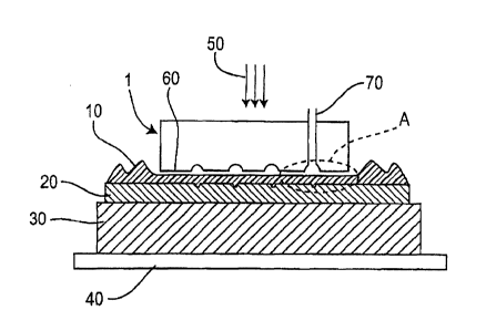
BRIEF DESCRIPTION OF THE FIGURES
Figure 1 illustrates a dielectric film coating on a substrate positioned
between a
compression tool (~,, a planarization object) and a compliant support, wherein
the
compression tool is equipped with a purge inlet.
Figure 2 illustrates a dielectric film coating on a substrate positioned
between a
compression tool and a compliant support, where the substrate and film have a
convex
surface and the compression tool is positioned to make initial contact at the
center of
the film.
Figure 3 illustrates the relationship between an individual die bearing scribe
lines and
purge channels in the press and compression tool purge channels matching the
inter-
substrate scribe lines.
9
CA 02384463 2002-03-08
WO 01/18860 PCT/US00/24847
Figure 4 illustrates the operational relationship between purge inlet
structure and the
purge channels in a substrate and compression tool in removing vapors or gases
from
the pressed dielectric film.
Figure 5 illustrates the injection of vapors, gases etc. through vent
channels.
Figure 6 illustrates an array of compression tools that are smaller in size
than the
substrate, so as to impress multiple patterns or planar regions into a
dielectric coating
on different parts of a single substrate.
Figure 7 illustrates one embodiment of the inventive apparatus placed in an
arbor
press.
CA 02384463 2002-03-08
WO 01/18860 PCT/US00/24847
DETAILED DESCRIPTION OF THE PREFERRED EMBODIMENT
Accordingly, methods and apparatus for planarizing and embossing useful
topography
onto dielectric film coatings on substrates and devices are provided, together
with
devices fabricated by the inventive methods.
In order to better appreciate the scope of the invention, it should be
understood that
unless the "Si02" functional group is specifically mentioned when the term
"silica" is
employed, the term "silica" as used herein, for example, with reference to
nanoporous
dielectric films, is intended to refer to dielectric films prepared by the
inventive
methods from an organic or inorganic glass base material, e.~T., any suitable
starting
material containing one or more silicon-based dielectric precursors. It should
also be
understood that the use of singular terms herein is not intended to be so
limited, but,
where appropriate, also encompasses the plural, e_g., exemplary processes of
the
invention may be described as applying to and producing a "film" but it is
intended
that multiple films can be produced by the described, exemplified and claimed
processes, as desired.
Additionally, the term "aging" refers to the gelling or polymerization, of the
combined silica-based precursor composition on the substrate after deposition,
induced, ~, by exposure to water and/or an acid or base catalyst. Gelling is
optionally applied to precursors selected to form foamed, i.e., nanoporous
dielectric
films, and/or nonporous dielectric films. Gelling can be accomplished by the
above-
described crosslinking and/or evaporation of a solvent.
The term "curing" refers to the hardening and drying of the film, after
gelling,
typically by the application of heat, although any other art-known form of
curing may
be employed, e~, by the application of energy in the form of an electron beam,
ultraviolet radiation, and the like.
11
CA 02384463 2002-03-08
WO 01/18860 PCT/US00/24847
The terms, "agent" or "agents" herein should be considered to be synonymous
with the terms,
"reagent" or "reagents," unless otherwise indicated.
Further, although the description provided herein generally describes
processes and
apparatus employed for preparing and planarizing or embossing patterns onto
foamed dielectric materials, such as the exemplified nanoporous silica films,
the artisan
will readily appreciate that the instantly provided methods and compositions
are
optionally applied to other substrate surfaces, and that other planarizing
materials can be
employed, including, for example, nonporous silica dielectric films and
organic polymer-
based dielectric films.
In addition, the terms, "flat" or "planar" are intended to be equivalent,
unless otherwise
stated, when used herein. When these terms are employed with reference to a
dielectric
film produced by the inventive methods, it is to indicate that the film has
the desired
degree of planarization.
Absent any statement to the contrary, reference herein to a "planarization
object" and/or
"planarization surface" or "compression tool" is intended to encompass objects
or
surfaces bearing any useful topography, including a simple plane, a set of two
or more
planar regions and/or any other suitable pattern to be embossed or impressed
on a
nanoporous dielectric silica film.
In addition, any suitable art-known objects can be used as planarization
objects or
compression tools to emboss or impress a plastic or malleable dielectric film
surface with
a topographical pattern, i.e., including one or more planar impressions.
Planarization
objects can have at least one flat surface, such as optical flats and the
like, or have a
contact surface that is curved in one of its dimensions, including drums,
rollers, or more
complex curved surfaces. Thus, for planarization objects having curved
surfaces, it will
be appreciated that contact between such a curved surface and the surface to
be treated
will be achieved with a rolling motion or rotating motion. In addition, it
will be
12
CA 02384463 2002-03-08
WO 01/18860 PCT/US00/24847
understood that the planarization object is typically incorporated into any
art-known
press or roller device to provide the mechanical force necessary to conduct
the
compression step according to the invention.
Broadly, a substrate coating can be contacted with a planarization object
before,
during or after the aging and/or curing of the applied dielectric film. It is
simply
required that the applied film or coating be sufficiently plastic or pliable
to accept the
planar impression, without damaging or preventing formation of desirable
features,
e.~., the nanometer-scale pore structure of silica dielectric films, when that
feature is
desired.
It will also be appreciated that the planarization processes and apparatus
provided by
the invention can optionally provide a nanoporous dielectric silica film
having a
sealed film surface, which can provide the added benefits of improved
mechanical
properties, e~, increased cohesive strength, modulus, or adhesion, relative to
nonplanarized films, and optionally can obviate a need for post-curing surface
modification to enhance surface hydrophobic properties.
A. METHODS FOR PREPARING DIELECTRIC FILMS
Dielectric films, ~, interlevel dielectric coatings, are prepared from
suitable
precursors applied to a substrate by any art-known method, including spin-
coating,
dip coating, brushing, rolling, spraying and/or by chemical vapor deposition.
The
precursor can be an organic polymer precursor, a silicon-based precursor
and/or
combinations thereof. The coating is then processed to achieve the desired
type and
consistency of dielectric coating, wherein the processing steps are selected
to be
appropriate for the selected precursor and the desired final product.
Typically, silicon-based dielectric films, including nanoporous silica
dielectric films,
are prepared from a suitable silicon-based dielectric precursor, e.~., a spin-
on-glass
13
CA 02384463 2002-03-08
WO 01/18860 PCT/US00/24847
("S.O.G.") material blended with one or more solvents and/or other components.
The
dielectric precursor is applied to a surface to be planarized by any art-known
method,
~, including, but not limited to, spin-coating, dip coating, brushing,
rolling, spraying
and/or by chemical vapor deposition. Prior to application of the base
materials to form
the dielectric film, the substrate surface is optionally prepared for coating
by standard,
art-known cleaning methods.
After the precursor is applied to the substrate surface, the coated surface is
contacted
with a planarization object, i.e., in the form of a compression tool, for a
time and at a
I O pressure effective to transfer the desired pattern to the dielectric
coating or film on the
substrate surface .
Preferably, the contact surface of the object is fabricated or coated with a
non-stick
release material, e_.~, TeflonTM or its functional equivalent. This can be in
the form of
a removable film or sheet of release material. Alternatively, the release
material can
be provided as a release coating directly on the compression tool working
surface.
The release material or coating can include any art-known materials, g_gs,
fluorocarbons, hydrocarbons, or other organic and/or inorganic materials which
are
either liquid or solid.
Optionally, the release material is selectively permeable, e_.,g_, composed of
or
including GortexTM and is able to pass vapor phase reagents, dissolved gases,
reaction
product gases, and/or solvents into or away from the surface being compressed.
Advantageously, such a selectively permeable membrane can prevent the
formation
of bubble artifacts on or within the planarized surface. Such a selectively
permeable
non-stick surface can also optionally be replaced or undercoated with a
material that
is selected to absorb and/or adsorb gases or vapors that might lead to
undesirable
formation of bubbles on the pressed surface. In another option, the contact
surface of
the compression tool incorporates one or more openings or passages to allow
for
14
CA 02384463 2002-03-08
WO 01/18860 PCT/US00/24847
venting of any excess vapors or gases and the release material is on the
working face
of the compression tool.
Once the surface of the treated dielectric film has assumed the desired shape,
the
compression tool and any non-stick release material are then separated from
the
dielectric film, although in certain embodiments an optional non-stick release
material
can be left on the substrate coating for an additional time period, to allow
more time
for aging or gelation, to allow for further film processing and/or to protect
the newly
planarized surface during further processing steps.
When the release material is a coating on the compression tool working
surface, the
release coating can optionally be dissolved or otherwise neutralized, allowing
ease of
separation of the compression tool from the planarized film. In one preferred
embodiment, the release material can be a material that is vaporized when
neutralized. The expanding vapor from the neutralized coating then assists in
pushing
the compression tool off of the planarized film. Vaporizable release materials
suitable for this purpose include, simply by way of example, polyalkylene
oxides or
PAOs, with molecular weights ranging from about 500 to about 5000. These types
of
polymers can be spin coated in a uniform thin film onto the working face of a
planarization object in its melted state (~100C melting point) or with a
solvent (such
as water or alcohol). The PAO is desirably solid at room temperature, to allow
a hard
contacting surface for planarization. After forming or gelling or both, the
PAO can be
melted for release, or further heated (> 100 C) to either vaporize or
thermally
decompose to form a vapor which can separate the parts. Preferred polyalkylene
oxide polymers include, simply by way of example, polyethylene oxides and/or
polyethylene glycols or PEGs, in the same general molecular weight range.
Yet another variation on release materials that can be volatized is to combine
a
material which is normally solid at room temperature, such as a PEG that can
be
compounded with a low to medium weight glycol or alcohol, and still remain as
a
CA 02384463 2002-03-08
WO 01/18860 PCT/US00/24847
solid compound at room temperature. The glycol components can then be easily
vaporized to allow release of the planarization flat from the dielectric film.
Common
petroleum based waxes also have similar properties and can perform the same
function.
Precursors for Dielectric Films
Examples of suitable dielectric precursors broadly include monomers, monomer
mixtures, oligomers, and oligomer mixtures that are solidified through curing
by
incorporated or applied reagents, heat, radiation and the like, and/or various
art-
known combinations thereof. Other examples of suitable materials include solid
materials such as polymer melts that can softened by heating, and then
resolidified
through cooling.
Or,~anic-Based Precursors for Dielectric Films
Organic polymer precursors that can optionally be employed to form planarized
or
embossed interlevel dielectric films using the methods and apparatus of the
invention
are well known and include, simply by way of example, polyimide precursors as
described, e.~., by U.S. patent numbers 4,113,550, 4,218,283 and 4,436,583,
all
incorporated herein by reference in their entireties. Preferred organic
dielectric
precursors include, simply by way of example, ethers of oligomeric phenol-
dialdehyde condensation products containing vinyl benzyl moieties in at least
half of
the ether moieties as described in co-owned U.S. patent number 4,908,096,
incorporated herein by reference in its entirety. Other preferred organic
polymers
include fluorinated and non-fluorinated polymers, in particular fluorinated
and non-
fluorinated poly(arylethers) available under the tradename FLARETM from
Honeywell
International Inc., and copolymers mixtures thereof. The polymer component is
preferably present in an amount of from about 10 % to about 30 % by weight of
the
composition. A more preferred range is from about 15 % to about 30 % and most
preferably from about 17 % to about 25 % by weight of the composition.
16
CA 02384463 2002-03-08
WO 01/18860 PCT/US00/24847
Epoxy resins are additional examples of dielectric precursors that are suited
for use in
the present process. One example of a suitable epoxy resin is epoxy novolac
431
(DEN-431) which is commercially obtained from the Dow Chemical Co. The uncured
resin has a viscosity of about 100 cp at a temperature of 100°C. The
resin is cured at a
temperature of about 100°C in the presence of an acid catalyst. An
example of a
suitable acid catalyst is the photoacid generator triphenylsulphonium
hexafluoroantimonate.
Silicon-Based Precursors for Dielectric Films
Preferred silicon-based dielectric precursors include organosilanes,
including, for
example, alkoxysilanes according to Formula I, as taught, e_.g_, by co-owned
U.S.
serial number 09/054,262, filed on April 3, 1998, the disclosure of which is
incorporated by reference herein in its entirety.
17
CA 02384463 2002-03-08
WO 01/18860 PCT/US00/24847
R
R-Si-R Formula I
R
In one embodiment, Formula I is an alkoxysilane wherein at least 2 of the R
groups
are independently C, to C4 alkoxy groups, and the balance, if any, are
independently
selected from the group consisting of hydrogen, alkyl, phenyl, halogen,
substituted
phenyl. For purposes of this invention, the term alkoxy includes any other
organic
group which can be readily cleaved from silicon at temperatures near room
temperature by hydrolysis. R groups can be ethylene glycoxy or propylene
glycoxy or
the like, but preferably all four R groups are methoxy, ethoxy, propoxy or
butoxy.
The most preferred alkoxysilanes nonexclusively include tetraethoxysilane
(TEOS)
and tetramethoxysilane. As exemplified below, a partially hydrolyzed and
partially
condensed fluid alkoxysilane composition can be employed. Such a precursor is
commercially available as NanoglassTM K2.2 (Honeywell International Inc.,
Advanced Micoelectronic Materials).
In a further option, for instance, especially when the precursor is applied to
the
substrate by chemical vapor deposition, e.~., as taught by co-owned patent
application
serial number 091111,083, filed on July 7, 1998, and incorporated by reference
herein
in its entirety, the precursor can also be an alkylalkoxysilane as described
by Formula
I, but instead, at least 2 of the R groups are independently C, to C4
alkylalkoxy groups
wherein the alkyl moiety is C, to C4 alkyl and the alkoxy moiety is C, to C6
alkoxy,
or ether-alkoxy groups; and the balance, if any, are independently selected
from the
group consisting of hydrogen, alkyl, phenyl, halogen, substituted phenyl. In
one
preferred embodiment each R is methoxy, ethoxy or propoxy. In another
preferred
embodiment at least two R groups are alkylalkoxy groups wherein the alkyl
moiety is
18
CA 02384463 2002-03-08
WO 01/18860 PCT/US00/24847
C, to C4 alkyl and the alkoxy moiety is C, to C6 alkoxy. In yet another
preferred
embodiment for a vapor phase precursor, at least two R groups are ether-alkoxy
groups of the formula (C, to C6 alkoxy)~ wherein n is 2 to 6.
Application serial number 09/111,083, mentioned above, also teaches that
preferred
silica precursors for chemical vapor deposition include, for example, any or a
combination of alkoxysilanes such as tetraethoxysilane, tetrapropoxysilane,
tetraisopropoxysilane, tetra(methoxyethoxy)silane,
tetra(methoxyethoxyethoxy)silane
which have four groups which may be hydrolyzed and than condensed to produce
silica, alkylalkoxysilanes such as methyltriethoxysilane silane,
arylalkoxysilanes such
as phenyltriethoxysilane and precursors such as triethoxysilane which yield
SiH
functionality to the film. Tetrakis(methoxyethoxyethoxy)silane,
tetrakis(ethoxyethoxy)silane, tetrakis(butoxyethoxyethoxy)silane, tetrakis(2-
ethylthoxy)silane, tetrakis(methoxyethoxy)silane, and
1 S tetrakis(methoxypropoxy)silane are particularly useful for the invention.
Additionally, partially hydrolyzed, condensed or polymerized derivatives of
these
species can be used in this invention. Other precursors of utility to this
invention
could include precursors which can be cross-linked by exposure to heat or
light. In
general, the precursors can be gases, liquids or solids at room temperature.
In other preferred embodiments, the silicon-based dielectric precursors) can
also be
selected from one or more additional polymers, as taught by co-owned U.S.
serial
number, 60/098,515, f led on August 31, 1998, and incorporated by reference
herein
in its entirety, including, but not limited to, a silsesquioxane polymer,
hydrogensiloxanes which have the formula [(HSi0,.5)XOy]~,
hydrogensilsesquioxanes
which have the formula (HSiO,.s)~, and hydroorganosiloxanes which have the
formulae [(HSi0,.5)XOY(RSi0,,5)ZJ~, [(HSi0,.5)X(RSi0,.5)y]~ and
[(HSi0,.5)XOy(RSiO,.s)Z]~. In each of these polymer formulae, x is about 6 to
about
20, y is 1 to about 3, z is about 6 to about 20, n ranges from 1 to about
4,000, and each
R is independently H, C, to Cg alkyl or C6 to C,Z aryl. The weight average
molecular
19
CA 02384463 2002-03-08
WO 01/18860 PCT/US00/24847
weight may range from about 1,000 to about 220,000. In the preferred
embodiment n
ranges from about 100 to about 800 yielding a molecular weight of from about
5,000
to about 45,000. More preferably, n ranges from about 250 to about 650
yielding a
molecular weight of from about 14,000 to about 36,000. Thus, useful silicon-
based
polymers nonexclusively include hydrogensiloxane, hydrogensilsesquioxane,
hydrogenmethylsiloxane, hydrogenethylsiloxane, hydrogenpropylsiloxane,
hydrogenbutylsiloxane, hydrogentert-butylsiloxane, hydrogenphenylsiloxane,
hydrogenmethylsilsesquioxane, hydrogenethylsilsesquioxane,
hydrogenpropylsilsesquioxane, hydrogenbutylsilsesquioxane, hydrogentert-
butylsilsesquioxane and hydrogenphenylsilsesquioxane and mixtures thereof, as
well
as others too numerous to mention.
In further preferred embodiments, as taught by co-owned U.S. serial number
60/098,068, filed on August 27, 1998, incorporated by reference herein in its
entirety,
the silica precursors) can also be formed by reacting certain multifunctional
silane
reagents prior to application of the reaction product to a substrate. For
example, such
precursors are formed by reacting a multifunctional, ,e.~., a tri-functional
silane
precursor, with a tetra-functional silane precursor and then depositing the
reaction
product on a substrate.
Desirable mufti-functional alkoxysilanes are selected from the group having
the
formula
An-SiHm Formula II
wherein each A is independently an alkoxy (O-R) wherein R is an organic moiety
independently selected from the group consisting of an alkyl and an aryl, and
wherein
n is an integer ranging from 1 to 3; m is an integer ranging from 1 to 3 and
the sum of
mandnis4.
A tetra-functional alkoxylsilane employed in the processes of the invention
preferably
has a formula of
CA 02384463 2002-03-08
WO 01/18860 PCT/US00/24847
A4 Si Formula III
wherein each A is independently an alkoxy (O-R) and R is an organic moiety
independently selected from the group consisting of an alkyl and an aryl,
In a further aspect of the invention, the alkoxysilane compounds described
above may
be replaced, in whole or in part, by compounds with acetoxy and/or halogen-
based
leaving groups. For example, the precursor compound may be an acetoxy
(CH3-CO-O-) such as an acetoxy-silane compound and/or a halogenated compound,
e.g., a halogenated silane compound and/or combinations thereof. For the
halogenated precursors the halogen is, e~,g" Cl, Br, I and in certain aspects,
will
optionally include F.
A low organic content alkoxysilane useful in forming dielectric films include
those of
formulas IV - VII, below, where the carbon containing substituents are present
in an
amount of less than about 40 mole percent.
[H-Si01,5]n[R-Si01,5]m , Formula IV
[H0.4-I.OSi01,5 - 1.8]n[R0.4-1.0-Si01,5 - 1.8]m ~ Formula V
[HO-1.0-5101.5-2.0]n[R-Si01,5]m , Formula VI
[H-Si01,5]x[R-Si01.5]y[Si02]z Formula VII
wherein the sum of n and m, or the sum or x, y and z is from about 8 to about
5000,
and m and y are selected such that carbon containing substituents are present
in an
amount of less than about 40 mole percent. R, is selected from substituted and
unsubstituted straight chain and branched alkyl groups, cycloalkyl groups,
substituted
and unsubstituted aryl groups, and mixtures thereof. The specific mole percent
of
carbon containing substituents is a function of the ratio of the amounts of
starting
materials. In a preferred embodiments the mole percent of carbon containing
substituents is in the range of from about 15 mole percent to about 25 mole
percent.
These polymers are described more fully in U.S. patent application serial
number
21
CA 02384463 2002-03-08
WO 01/18860 PCT/US00/24847
09/044,831, filed March 20, 1998, which is incorporated herein by reference. A
suitable low organic content polymer precursor is available commercially as
LOSPTM
(Honeywell International Inc. at Santa Clara, California).
A high organic content alkoxysilane useful in forming dielectric films include
those
of formulas wherein the carbon containing substituents are present in an
amount of
about 40 mole percent or more. These polymers are described more fully in co-
owned
U.S. patent application serial number 09/044,798, filed March 20, 1998, which
is
incorporated herein by reference. Such have the formulae VIII-X:
[HSi01,5]n [RSi01.5]m , Formula VIII
[H0.4-I.OSi01,5-1.8]n [R0.4-I.OSi01.5-1.8]m , Formula IX
[HO-I.OSi01.5-2.0]n [RSi01_5]m , Formula X
wherein the sum of n and m is from about 8 to about 5000 and m is selected
such that
the carbon containing substituent is present in an amount of from about 40
Mole
percent or greater; and
[HSi01,5]x [RSi01,5]y [Si02]z; Formula XI
wherein the sum of x, y and z is from about 8 to about 5000 and y is selected
such
that the carbon containing substituent is present in an amount of about 40
Mole % or
greater; and wherein R is selected from substituted and unsubstituted straight
chain
and branched alkyl groups, cycloalkyl groups, substituted and unsubstituted
aryl
groups, and mixtures thereof. The specific mole percent of carbon containing
substituents is a function of the ratio of the amounts of starting materials.
A suitable
high organic content polymer precursor is available commercially as HOSPTM
(Honeywell International Inc.at Santa Clara, California).
Polymers of the structures IV-XI may be prepared by mixing a solution of at
least one
organotrihalosilane and hydridotrihalosilane to form a mixture; combining the
mixture with a dual phase solvent which includes both a non-polar solvent and
a polar
22
CA 02384463 2002-03-08
WO 01/18860 PCT/US00/24847
solvent; adding a catalyst to the dual phase solvent and trihalosilane
mixture, thus
providing a dual phase reaction mixture; reacting the dual phase reaction
mixture to
produce an organohydridosiloxane; and recovering the organohydridosiloxane
from
the non-polar portion of the dual phase solvent system. Additional information
on
preparation of these polymers is provided by co-owned U.S. Patent Application
serial
number 09/328,648, filed on June 9, 1999, the disclosure of which is
incorporated by
reference herein in its entiretv.
Generally for the above-described base materials or dielectric film
precursors, the
polymer component is preferably present in an amount of from about 10 % to
about 50
by weight of the composition. A more preferred range is from about 15 % to
about 30
and most preferably from about 17 % to about 25 % by weight of the
composition.
Preferred siloxane materials are commercially available, for example, from
Honeywell International Inc. under the tradename Accuglass~.
23
CA 02384463 2002-03-08
WO 01/18860 PCT/US00/24847
Su trates
Broadly speaking, a "substrate" as described herein includes any suitable
composition
formed before a nanoporous silica film of the invention is applied to and/or
formed on
that composition. For example, a substrate is typically a silicon wafer
suitable for
producing an integrated circuit or related device, and the base material from
which the
nanoporous silica film is formed is applied onto the substrate by conventional
methods, e_.~, including, but not limited to, the art-known methods of spin-
coating,
dip coating, brushing, rolling, spraying and/or chemical vapor deposition, or
other
suitable method or methods. Prior to application of the base materials to form
the
nanoporous silica film, the substrate surface is optionally prepared for
coating by
standard, art-known cleaning methods.
Suitable substrates for the present invention non-exclusively include
semiconductor
materials such as gallium arsenide ("GaAs"), silicon and compositions
containing
silicon such as crystalline silicon, polysilicon, amorphous silicon, epitaxial
silicon,
and silicon dioxide ("Si02") and mixtures thereof, e.g., in the form of a
polished
wafer. The substrate surface typically includes an optional pattern of raised
lines,
such as metal, oxide, nitride or oxynitride lines which are formed by well
known
lithographic techniques. Suitable materials for the lines, that form the
conductors or
insulators of an integrated circuit, include silica, silicon nitride, titanium
nitride,
tantalum nitride, aluminum, aluminum alloys, copper, copper alloys, tantalum,
tungsten and silicon oxynitride. Such are typically closely separated from one
another at distances of about 20 micrometers or less, preferably 1 micrometer
or less,
and more preferably from about 0.05 to about 1 micrometer. Other optional
features
of the substrate surface include an oxide layer, such as an oxide layer formed
by
heating a silicon wafer in air, or more preferably, an Si02 oxide layer formed
by
chemical vapor deposition of such art-recognized materials as, e.~., plasma
enhanced
tetraethoxysilane ("PETEOS") silane oxide and combinations thereof, as well as
one
or more previously formed nanoporous silica dielectric films
24
CA 02384463 2002-03-08
WO 01/18860 PCT/US00/24847
The dielectric films can be applied so as to cover and/or lie between such
optional electronic
surface features, e~, circuit elements and/or conduction pathways. Such
optional substrate
features can also be applied above the nanoporous silica film of the invention
in at least one
additional layer, so that the low dielectric film serves to insulate one or
more, or a plurality of
electrically and/or electronically functional layers of the resulting
integrated circuit. Thus, a
substrate according to the invention optionally includes a silicon material
that is formed over
or adjacent to a nanoporous silica film of the invention, during the
manufacture of a
multilayer and/or multicomponent integrated circuit.
A. A~nlving a Silicon-Based Dielectric Precursor to a Substrate
Silicon-based dielectric films, including nanoporous silica dielectric films,
are
prepared by coating a silicon-based dielectric precursor onto a substrate or
substrates
using methods based upon those described in detail in, for example, in co-
owned U.S.
serial number 09/054,262, filed on April 3, 1998, the disclosure of which is
incorporated by reference herein in its entirety. Modifications to methods
described
in U.S. serial number 09/054,262, for example, include those that are those
optionally
required by the need for contacting the film material with a planarization
object.
Typically, a nanoporous silica dielectric film is prepared by forming a
reaction
product of, for example, at least one alkoxysilane, ~, as described by Formula
I,
supra, a solvent composition, optional water and an optional catalytic amount
of an
acid or base. Water is included to provide a medium for hydrolyzing the
alkoxysilane. Preferably the solvent composition comprises at least one
relatively
high volatility solvent and at least one a relatively low volatility solvent.
This reaction product is applied onto a substrate, as described supra. The
high
volatility solvent evaporates during and immediately after deposition of the
reaction
CA 02384463 2002-03-08
WO 01/18860 PCT/US00/24847
product. The reaction product is hydrolyzed and condensed until it forms a gel
layer.
For planarization, for example, a flat surface can be contacted with the gel
layer after
the high volatility solvent has evaporated, leaving behind a viscous coating,
but
before the curing or aging process has progressed sufficiently to render the
coating
non-pliable.
For purposes of the invention, "a relatively high volatility solvent" is one
which
evaporates at a temperature below, preferably significantly below that of the
relatively low volatility solvent. The relatively high volatility solvent
preferably has a
boiling point of about 120°C or less, preferably about 100°C or
less. Suitable high
volatility solvents nonexclusively include methanol, ethanol, n-propanol,
isopropanol,
n-butanol and mixtures thereof. Other relatively high volatility solvent
compositions
which are compatible with the other ingredients can be readily determined by
those
skilled in the art.
For purposes of the invention, "a relatively low volatility solvent"
composition is one
which evaporates at a temperature above, preferably significantly above, that
of the
relatively high volatility solvent. The relatively low volatility solvent
composition
preferably has a boiling point of about 175°C or higher, more
preferably about 200°C
or higher. Suitable low volatility solvent compositions nonexclusively include
alcohols and polyols including glycols such as ethylene glycol, 1,4-butylene
glycol,
1,5-pentanediol, 1,2,4-butanetriol, 1,2,3-butanetriol, 2-methyl-propanetriol,
2-
(hydroxymethyl)-1,3-propanediol, 1,4,1,4-butanediol, 2-methyl-1,3-propanediol,
tetraethylene glycol, triethylene glycol monomethyl ether, glycerol and
mixtures
thereof. Other relatively low volatility solvent compositions which are
compatible
with the other ingredients can be readily determined by those skilled in the
art.
In another option, acid catalysts can be employed. Suitable acids are nitric
acid and
compatible organic acids which are volatile, i.e. which evaporate from the
resulting
26
CA 02384463 2002-03-08
WO 01/18860 PCT/US00/24847
reaction product under the process operating conditions, and which do not
introduce
impurities into the reaction product.
The silane component, e.~., alkoxysilane, is preferably present in an amount
of from
about 3 % to about 50 % by weight of the overall blend. A more preferred range
is from
about 5 % to about 45 % and most preferably from about 10 % to about 40 %.
The solvent component is preferably present in an amount of from about 20 % to
about
90 % by weight of the overall blend. A more preferred range is from about 30 %
to
about 70 % and most preferably from about 40 % to about 60 %. The greater the
percentage of high volatility solvent employed, the thinner is the resulting
film. The
greater the percentage of low volatility solvent employed, the greater is the
resulting
porosity
The mole ratio of water to the silane component is preferably from about 0 to
about 50.
A more preferred range is from about 0.1 to about 10 and most preferably from
about 0.5
to about 1.5. The acid is present in a catalytic amount which can be readily
determined by those skilled in the art. Preferably the molar ratio of acid to
silane
ranges from about 0 to about 0.2, more preferably from about 0.001 to about
0.05, and
most preferably from about 0.005 to about 0.02.
The prepared silicon-based dielectric precursor is then coated on a substrate.
The
layer is relatively uniformly applied. While the substrate can be any art-
known
material, ~., as described supra, typical substrates are polished
semiconductor
wafers, optionally having one or more semiconductor components previously
fabricated on the surface.
The solvent, usually the higher volatility solvent is then at least partially
evaporated
from the coating. The more volatile solvent evaporates over a period of
seconds or
minutes. At this point, the film is a viscous liquid of the silica precursors
and the less
27
CA 02384463 2002-03-08
WO 01/18860 PCT/US00/24847
volatile solvent. Slightly elevated temperatures may optionally be employed to
accelerate this step. Such temperatures may range from about 20°C to
about 80°C,
preferably range from about 20°C to about 50°C and more range
from about 20°C to
about35°C.
The coated substrate is then placed in a sealed chamber and is rapidly
evacuated to a
vacuum. In the preferred embodiment, the pressure of the evacuated chamber
ranges
from about 0.001 torr to about 0.1 ton, or greater. In an alternative
embodiment, the
chamber pressure may range from about 0.001 torr to about 760 torr, or
greater.
Typically, the pressure is about 250 torr. Then the coating is sequentially
exposed to
both a water vapor and a base vapor, either simultaneously or sequentially.
For
purposes of this invention, a base vapor includes gaseous bases. Preferably
the
coating is first exposed to a water vapor and then exposed to a base vapor,
however,
in an alternate embodiment, the coating may first be exposed to a base vapor
and then
a water vapor. The first of the two exposures is conducted such that
thereafter the
pressure in the chamber remains at sub-atmospheric pressure. The second
exposure
may be conducted at atmospheric pressure, sub-atmospheric pressure or super-
atmospheric pressure.
In one preferred embodiment, after the coated substrate is placed in the
sealed
chamber and the chamber evacuated to a vacuum, a valve is opened to a
reservoir of
water, and water vapor quickly fills the chamber. The partial pressure of
water vapor,
PHZO is controlled by the length of time that the valve is open and the
temperature at
which the liquid water reservoir is maintained. Because of the low vapor
pressure of
water, the chamber pressure after water addition is much less than ambient.
The
pressure rise that occurs in the chamber during the water vapor addition is a
direct
measure of the water vapor partial pressure. In the preferred embodiment, the
pressure of the evacuated chamber after the water vapor exposure ranges from
about
0.1 torr to about 150 torr, preferably about 1 torr to about 40 ton and more
preferably
from about 5 torr to about 20 ton. In the preferred embodiment, the
temperature of
28
CA 02384463 2002-03-08
WO 01/18860 PCT/US00/24847
the water during the exposure ranges from about 10°C to about
60°C, preferably from
about 15°C to about 50°C, and more preferably from about
20°C to about 40°C. In the
preferred embodiment, the temperature in the chamber after water exposure
ranges
from about 10°C to about 50°C, preferably from about 15°C
to about 40°C, and more
preferably from about 20° C to about 40°C.
After water vapor addition, a base vapor is dosed into the chamber. The
chamber
pressure after base dosing may be at, above or below atmospheric pressure. If
the
pressure is above atmospheric, the chamber must be designed to resist the
total
system pressure. As with water vapor, the partial pressure of the base is
known
directly from the pressure rise during base dosing. Because the chamber only
contains base and water vapor, except for trace amounts of atmospheric gas
left from
the initial chamber pumpdown, the base and water diffusion rates are much
faster than
the case when evacuation is not conducted, resulting in greatly increased
polymerization rates, decreased process time per coated substrate, and greater
uniformity across the coated surface. Since the base and water vapor are added
separately, their partial pressures are easily measured and there is very
little waste.
Only the vapor above the wafer need be removed upon deposition. The order of
addition of water and base may be reversed but the addition of water before
the base
is preferred because of its lower vapor pressure. In the preferred embodiment,
the
pressure of the evacuated chamber after the base vapor exposure ranges from
about
100 torr to about 2,000 torn preferably about 400 torr to about 1,000 ton and
more
preferably from about 600 torr to about 800 torr. In the preferred embodiment,
the
temperature of the base during the exposure ranges from about 10°C to
about 60°C,
preferably from about 15°C to about 40°C, and more preferably
from about 20°C to
about 30°C. In the preferred embodiment, the temperature in the chamber
after base
exposure ranges from about 10°C to about 50°C, preferably from
about 15°C to about
40°C, and more preferably from about 20°C to about 40°C.
29
CA 02384463 2002-03-08
WO 01/18860 PC'f/US00/24847
Suitable bases (je., alkaline regents) for use in the base vapor
nonexclusively include
ammonia and non-volatile_amines, such as primary, secondary and tertiary alkyl
amines, aryl amines, alcohol amines and mixtures thereof which have a boiling
point
of about 200°C or less, preferably 100°C or less and more
preferably 25°C or less.
Preferred amines do not require an atmosphere for aging, i.e., while the film
is being
impressed with a flat surface, and include, for example, monoethanol amine,
tetraethylenepentamine, 2-(aminoethylamino)ethanol, 3-aminopropyltriethoxy
silane,
3-amino-1,2-propanediol, 3-(diethylamino)-1,2-propanediol, n-(2-aminoethyl)-3-
aminopropyl-trimethoxy silane, 3-aminopropyl-trimethoxy silane. Additional
amines
that are useful for the processes of the invention include, e.~., methylamine,
dimethylamine, trimethylamine, n-butylamine, n-propylamine, tetramethyl
ammonium hydroxide, piperidine and 2-methoxyethylamine. The ability of an
amine
to accept a proton in water is measured in terms of the basic constant Kb, and
pKe -
log Kb. In the preferred embodiment, the pKb of the base may range from about
less
than 0 to about 9. A more preferred range is from about 2 to about 6 and most
preferably
from about 4 to about 5.
Preferably, the mole ratio of water vapor to base vapor ranges from about 1:3
to about
1:100, preferably from about 1:5 to about 1:50, and more preferably from about
1:10
to about 1:30.
The water vapor causes a continued hydrolysis of the alkoxysilane alkoxy
groups, and
the base catalyzes condensation of the hydrolyzed alkoxysilane and serves to
increase
molecular weight until the coating gels and ultimately increases gel strength.
The
film is then dried in a conventional way by solvent evaporation of the less
volatile
solvent. Elevated temperatures may be employed to dry the coating in this
step. Such
temperatures may range from about 20°C to about 450°C,
preferably from about 50°C
to about 350°C and more preferably from about 175°C to about
320°C.
CA 02384463 2002-03-08
WO 01/18860 PCT/US00/24847
Optionally, additional process steps may be applied to the formed nanoporous
silica
dielectric film, including, for example, a solvent rinse, a surface
modification to
enhance hydrophobicity, and any other art-known process steps as required.
After the desired time of reaction after base addition, on the order of
seconds to a few
minutes, the chamber pressure is brought to atmospheric pressure. This can be
accomplished by either adding an inert gas such as nitrogen and opening the
chamber
or evacuating the base/water mixture via vacuum and backfilling with an inert
gas, or
even optionally venting the chamber with a non-inert gas, such as air.
Thus, a precursor is deposited on a wafer and the more volatile solvent
continues to
evaporate over a period of seconds. The wafer is placed in a sealed chamber at
ambient pressure. The chamber is opened to a vacuum source and the ambient gas
is
evacuated and the chamber pressure decreases well below the partial pressure
of
water vapor. In the next step, water vapor is added and the chamber pressure
increases. The pressure increase during that step is the water partial
pressure (PHZO)~
The base vapor, in this case ammonia, is introduced into the chamber and
polymerization is triggered. The pressure increase during this step is the
base partial
pressure (for example, PNH3), so that the total pressure in the chamber at the
end of the
ammonia addition cycle is the sum of the partial pressures of water vapor and
ammonia. After the desired time, the chamber pressure may be raised to ambient
by
filling with an inert gas, such as nitrogen as shown, or it may be first
evacuated to
vacuum and subsequently backfilled to ambient pressure.
As a result, a relatively high porosity, low dielectric constant, silicon
containing
polymer composition forms on the substrate surface. The silicon containing
polymer
composition preferably has a dielectric constant of from about 1.1 to about
3.5, more
preferably from about 1.3 to about 3.0, and most preferably from about 1.5 to
about
2.5. The pore size of silica composition ranges from about 1 nm to about 100
nm,
more preferably from about 2 nm to about 30 nm, and most preferably from about
3
31
CA 02384463 2002-03-08
WO 01/18860 PCT/US00/24847
nm to about 20 nm. The density of the silicon containing composition,
including the
pores, ranges from about 0.1 to about 1.9 g/cm2, more preferably from about
0.25 to
about 1.6 g/cm2, and most preferably from about 0.4 to about 1.2 g/cm2.
B. Methods of Producing Dielectric Film
Bv A~lving Base Material Mixed in Mid-Stream
In another preferred embodiment, the nanoporous silica dielectric film is
prepared by
coating a substrate with a silicon-based precursor composition that is pre-
mixed by
combining multiple streams of free-flowing component precursor reagents before
the
composition is applied to a substrate. In this embodiment, a nanoporous silica
dielectric film is formed on a substrate by
(i) combining a stream of a silicon-based precursor or base material, such as,
for
example, an alkoxysilane composition, with a stream of a base containing
catalyst
composition to form a combined composition stream; immediately depositing the
combined composition stream onto a surface of a substrate and exposing the
combined composition to water (in either order or simultaneously); and
planarizing
the film during the curing of the combined composition; or
(ii) combining a stream of a silicon-based precursor or base material, such
as, for
example, an alkoxysilane composition, with a stream of water to form a
combined
composition stream; immediately depositing the combined composition stream
onto a
surface of a substrate; and planarizing the film during the curing of the
combined
composition.
Methods (i) and (ii) are described in detail, absent the planarization
features of the
present invention, in co-owned U.S. serial number 09/140,855, filed on August
27,
1998, the disclosure of which is incorporated by reference herein in its
entirety.
Processes for the preparation of nanoporous dielectric silica films by mixing
streams
of components is summarized in greater detail, as follows. Modifications to
methods
32
CA 02384463 2002-03-08
WO 01/18860 PCT/US00/24847
described in U.S. serial number 09/140,855 are those optionally required by
the need
for contacting the film material with a planarization object.
The first step of this process is to prepare a base material in the form of a
mixture of
at least one precursor, such as an alkoxysilane, as described for Formula I,
supra, and
a solvent composition. The mixture is then discharged onto a suitable
substrate in the
form of a stream. In one preferred embodiment, the stream of alkoxysilane
composition is combined with a stream of water to form a combined composition
stream immediately prior to contacting the substrate.
In an alternate preferred embodiment, a combined composition stream is formed
from
a stream of the alkoxysilane composition and a stream of a base (i.e.
alkaline)
containing catalyst composition, e_.~, an amine compound, as described, supra.
The
combined composition stream is thereafter deposited onto a surface of a
substrate.
Optionally, the combined composition stream is deposited onto the substrate
and is
then exposed to the water, in the form of a water vapor atmosphere.
Alternatively, the
combined composition stream is exposed to the water before deposition onto the
substrate. In yet another option, the combined composition stream is
simultaneously
exposed to the water and deposited onto the substrate. This may be in the form
of a
water stream or a water vapor atmosphere. After deposition and water exposure,
the
combined composition may be cured, aged, or dried before, during or after
planarization, to thereby form a nanoporous dielectric coating on the
substrate.
Whichever of the above options is selected for conducting the process, the
above-
described components of the combined stream composition contact each other in
the
space above the surface of the substrate, immediately prior to deposition. At
a point
of confluence of the individual streams, the combined stream is unbounded by
tubing,
piping, manifolds or the like. This minimizes reaction time between the
components
prior to deposition and prevents reaction within the intersection point of
supply tubes.
33
CA 02384463 2002-03-08
WO 01/18860 PCT/US00/24847
Preferably, the components are all in a liquid form and any suitable apparatus
for
distributing the liquid components may be used for depositing the above-
described
combined streams of, g~, alkoxysilane, water and base compositions according
to the
present invention. Suitable apparatus includes, for example, syringe pumps,
but the
artisan will appreciate that other devices may be used to form the combined
composition stream. Such nonexclusively include faucets, sprayers, hoses,
tanks,
pipes, tubes, and the like. Various methods of combining the components may be
used, such as dripping, squirting, streaming, spraying, and the like.
Exemplary apparatus for conducting this process includes separate containers,
e.~. .,
tanks, for storing separate components until the process begins. Each
respective tank
has a corresponding separate discharge tube for discharging the respective
component
to be combined into a single stream, so that the combined stream can be
deposited
onto a substrate surface. Each component is propelled through its respective
discharge tube by, e.~., gravity feed and/or by the action of one or more
pumps. The
artisan will also appreciate that the apparatus can also provide for
propelling one or
more components) by applying positive gas or air pressure to the corresponding
storage tank. The flow through each respective discharge tube is optionally
regulated
by one or more flow control valves located between the distal end of each
discharge
tube and its respective tank and/or by control of the pumping action, when
pumps are
employed to propel flow of components. If the components are propelled by air
or
gas pressure, component flow can also be regulated, in whole or in part, by
controlling the pressure of the air or gas propellant.
The discharge tubes are positioned so that each of the respective discharge
streams
combine together to form a combined composition stream, which is deposited
onto a
surface of a substrate positioned to received the combined composition stream.
Optionally, each discharge tube may also include a shaped nozzle, e~., a
spinner
nozzle, or a nozzle formed of one or more openings, ~,, analogous to a
showerhead,
suitable for forming a discharge stream that mixes well with other such
streams. The
34
CA 02384463 2002-03-08
WO 01/18860 PCT/US00/2484~
artisan will appreciate that the dimensions of any provided nozzle, and/or the
discharge end of each discharge tube, can be readily modified to assist in
regulating
pressure and flow rate for each stream, to assure optimal stream contact,
mixing, and
spreading of the resulting mixed composition stream over the substrate,
depending,
for example, upon the rate at which the process is conducted, the reaction
speed, and
the viscosity of the respective component.
A variety of processes may be employed by this method to form a nanoporous
dielectric film on a substrate. For a two-component process the components can
be,
for example, alkoxysilane composition and water, each stored in a separate
tank until
needed, or alternatively, a base containing catalyst composition in place of
the water
component.
For a three-component process, the apparatus can have three separate tanks
each with
a corresponding discharge tube for discharging one of three components, e~, an
alkoxysilane composition, a base containing catalyst composition, and water,
respectively. Additional storage tanks and discharge tubes can be added, if
required
to deliver additional components) for the selected process.
For example, when the combined stream is formed of alkoxysilane and base
catalyst,
the combined stream can be deposited on a substrate positioned in a closed
environment that includes a water vapor atmosphere. The closed environment can
be
formed by any suitable chamber or enclosure able to contain the substrate and
vapor
component(s). The enclosure will have an inlet or inlets for the component
discharge
tubes. Preferably, the enclosure portion of the apparatus will also include an
additional inlet, with an optional valve, to admit a vapor, a gas-vapor
mixture or
optionally a liquid to be converted to vapor within the enclosure.
For example, with a two-component combined stream as described above, the
apparatus will be constructed as broadly described above, with the additional
CA 02384463 2002-03-08
WO 01/18860 PCT/US00/24847
components of a source of water vapor is provided, e_.gt, an evaporation
bottle or
chamber, the evaporation bottle preferably including a heat source for
promoting
water vaporization and optionally a source of flowing air or inert gas to
carry the
water vapor into the enclosure. With the enclosure of the substrate, this
apparatus
operates to expose the combined composition stream to water either during or
after
deposition onto a surface of the enclosed substrate. The enclosure will also
optionally include outlets to allow for venting and/or recycling of the
unreacted water
vapor and/or other unreacted components.
Useful alkoxysilanes include those defined as for Formula I, supra. Also as
defined
supra, preferred alkoxysilanes nonexclusively include tetraethoxysilane (TEOS)
and
tetramethoxysilane.
The solvent composition for the base component, e.~., an alkoxysilane,
preferably
comprises a relatively high volatility solvent or a relatively low volatility
solvent or
both a relatively high volatility solvent and a relatively low volatility
solvent. The
solvent, usually the higher volatility solvent, is at least partially
evaporated
immediately after deposition onto the substrate. This partial drying leads to
better
planarity, even absent the additional planarization steps of the instant
invention, due
to the lower viscosity of the material after the first solvent or parts of the
solvent
comes off. The more volatile solvent evaporates over a period of seconds or
minutes.
Slightly elevated temperatures may optionally be employed to accelerate this
step.
Such temperatures preferably range from about 20°C to about
80°C, more preferably
from about 20°C to about 50°C and most preferably from about
20°C to about 35°C.
The meaning of the expressions, "a relatively high volatility solvent" and "a
relatively
low volatility solvent composition" is as defined in Section A, supra.
36
CA 02384463 2002-03-08
WO 01/18860 PCT/US00/24847
The alkoxysilane component is preferably present in an amount of from about 3
% to
about ~0 % by weight of the overall blend, more preferably from about 5 % to
about 45
and most preferably from about 10 % to about 40 %.
The solvent component of the alkoxysilane precursor composition is preferably
present
in an amount of from about 20 % to about 90% by weight of the overall blend,
more
preferably from about 30 % to about 70 % and most preferably from about 40 %
to about
60 %. When both a high and a low volatility solvent are present, the high
volatility
solvent component is preferably present in an amount of from about 20 % to
about 90
by weight of the overall blend, more preferably from about 30 % to about 70 %
and a
most preferably from about 40 % to about 60 % by weight of the overall blend.
When
both a high and a low volatility solvent are present, the low volatility
solvent component
is preferably present in an amount of from about 1 to about 40 % by weight of
the overall
blend, more preferably from about 3 % to about 30% and a most preferably from
about 5
% to about 20 % by weight of the overall blend.
The base containing catalyst composition contains a base, or a base plus
water, or a
base plus an organic solvent, or a base plus both water and an organic
solvent. The
base is present in a catalytic amount which can be readily determined by those
skilled
in the art. Preferably the molar ratio of base to silane ranges from about 0
to about
0.2, more preferably from about 0.001 to about 0.05, and most preferably from
about
0.005 to about 0.02. Water is included to provide a medium for hydrolyzing the
alkoxysilane. The mole ratio of water to silane is preferably from about 0 to
about 50,
more preferably from about 0.1 to about 10 and a most preferably from about
0.5 to
about 1.5. Suitable solvents for the base containing catalyst composition
include those
listed above as a high volatility solvent. Most preferred solvents are
alcohols such as
ethanol and isopropanol.
The temperature of the water during the exposure preferably ranges from about
10°C
to about 60°C, more preferably from about 15°C to about
50°C, and most preferably
37
CA 02384463 2002-03-08
WO 01/18860 PCT/US00/24847
from about 20°C to about 40°C. The temperature of the base
during the exposure
preferably ranges from about 10°C to about 60°C, more preferably
from about 1 S°C to
about 40°C, and most preferably from about 20°C to about
30°C.
Suitable bases nonexclusively include ammonia and amines, such as primary,
secondary and tertiary alkyl amines, aryl amines, alcohol amines and mixtures
thereof
which have a preferred boiling point of at least about -50°C, more
preferably at least
about 50°C, and most preferably at least about 150°C. Suitable
amines, in addition to
those recited supra, also include, alcoholamines, alkylamines, methylamine,
dimethylamine, trimethylamine, n-butylamine, n-propylamine, tetramethyl
ammonium hydroxide, piperidine, 2-methoxyethylamine, mono-, di- or
triethanolamines, and mono-, di-, or triisopropanolamines.
The combined composition may be cured, aged, or dried in a conventional way
such
as solvent evaporation of the less volatile solvent. Elevated temperatures may
be
employed to cure, age or dry the coating. Such temperatures preferably range
from
about 20°C to about 450°C, more preferably from about
50°C to about 350°C and most
preferably from about 175°C to about 320°C.
As a result, a relatively high porosity, low dielectric constant silicon
containing
polymer composition is formed on the substrate. The silicon containing polymer
composition preferably has a dielectric constant of from about 1.1 to about
3.5, more
preferably from about 1.3 to about 3.0, and most preferably from about 1.5 to
about
2.5. The pore size of silica composition preferably ranges from about 1 nm to
about
100 nm, more preferably from about 2 nm to about 30 nm, and most preferably
from
about 3 nm to about 20 nm. The density of the silicon containing composition,
including the pores, preferably ranges from about 0.1 to about 1.9 g/cm2, more
preferably from about 0.25 to about 1.6 g/cm2, and most preferably from about
0.4 to
about 1.2 g/cm2.
38
CA 02384463 2002-03-08
WO 01/18860 PCT/US00/24847
PAGE INTENTIONALLY LEFT BLANK
39
CA 02384463 2002-03-08
WO 01/18860 PCT/US00/24847
C. Variations on Film Forming Processes
Variations on and modifications to the above-described processes for
fabricating a
nanoporous silica dielectric film have been described in a number of co-owned
U.S.
patent applications and may optionally be utilized in the practice of the
instant
invention.
For example, the above-described methods may be modified by producing a film
with
at least two-different regions of density, i-e., adjacent regions of
relatively high and
relatively lower density, as disclosed by co-owned U.S. serial numbers
09/046,473
and 09/046,475, both filed on March 25, 1998, the disclosures of which are
incorporated by reference herein in their entireties.
In a second variation, water and base vapor mixing efficiencies are improved
by
blending at least one alkoxysilane with a solvent composition and optional
water and
1 S applying the blend to a semiconductor substrate and sequentially exposing
the
substrate to water vapor and a base vapor, in either order, at a pressure
below
atmospheric pressure, as disclosed by co-owned U.S. 09/054,262, filed on April
3,
1998, the disclosure of which is incorporated by reference herein in its
entirety.
In a third variation, a precursor mixture is formed of a relatively low
volatility solvent
composition that includes a C, to C4 alkylether of a C, to C4 alkylene glycol
which is
miscible in water, and alkoxysilanes as disclosed by co-owned U.S. serial
numbers
09/111,081, 09/111,082, both filed on July 7, 1998, the disclosures of which
are
incorporated by reference herein in their entireties.
In a fourth variation, silica precursors, as defined above by, g~, Formula I
and the
associated enumeration of preferred silica species, are deposited from the
vapor
phase, with an optional co-solvent, on a substrate to form a liquid-like film.
Further
details are provided by co-owned U.S. serial number 09/111,083, filed on July
7,
1998, the disclosure of which is incorporated by reference herein in its
entirety.
CA 02384463 2002-03-08
WO 01/18860 PCT/US00/24847
In a fifth variation, a uniform nanoporous dielectric film can be formed from
a liquid
alkoxysilane precursor spin-deposited onto a horizontally positioned flat
substrate
centered and held within a cup having an open top section and a removable
cover for
closing the top. Further details are provided by co-owned U.S. serial number
60/095,573, filed on August 6, 1998, the disclosure of which is incorporated
by
reference herein in its entirety.
In a sixth variation, a precursor composition is formed from an alkoxysilane,
an acid,
and a solvent composition containing a high volatility and low volatility
solvent. The
relatively high volatility solvent is evaporated, and the low volatility
solvent is
partially evaporated from the precursor composition. Further details are
provided by
co-owned U.S. serial number 09/234,609, filed on January 21, 1999, the
disclosure of
which is incorporated by reference herein in its entirety.
In a seventh variation, a suitable substrate that includes a dielectric film
is treated in a
substantially oxygen free environment by heating the substrate to a
temperature of
about 350°C or greater, for a time period of at least about 30 seconds.
Further details
are provided by co-owned U.S. serial number 60/098,515, filed on August 31,
1998,
the disclosure of which is incorporated by reference herein in its entirety.
In an eighth variation, a substantially uniform alkoxysilane gel composition
that
includes a combination of at least one alkoxysilane, an organic solvent
composition,
water, and an optional base catalyst is formed on a substrate. The substrate
is heated
in an organic solvent vapor atmosphere to condense the gel composition,
followed by
curing, as described by co-owned U.S. serial number 09/141,287, filed on
August 27,
1998, the disclosure of which is incorporated by reference herein in its
entirety.
In a ninth variation, nanoporous silica dielectric coatings are formed on a
substrate
via chemical vapor deposition of a precursor. The deposited precursor is then
41
CA 02384463 2002-03-08
WO 01/18860 PCT/US00/24847
exposed to a gelling agent, ~, water vapor, and either an acid or a base
vapor; and
dried to form a relatively high porosity, low dielectric constant, silicon
containing
polymer composition on the substrate as described by co-owned U.S. serial
number
09/111,083, filed on July 7, 1998, the disclosure of which is incorporated by
reference
herein in its entirety.
D. Surface Modification Reagents and Methods
Typically, the silica-based materials, such as the alkoxysiloxanes mentioned
herein, form
nanoporous films with surfaces, including surfaces of the pore structures,
that contain silanol
groups. Silanols and the water that they can adsorb from the air are highly
polarizable in an
electric field, and thus will raise the dielectric constant of the film. To
make nanoporous
films substantially free of silanols and water, an organic reagent, i.e., a
surface modification
agent, such as hexamethyldisilazane or methyltriacetoxysilane, is optionally
introduced into
the pores of the film. Such silylation reagent react with silanols on the pore
surfaces to add
organic, hydrophobic capping groups, e_.g" trimethylsilyl groups. Thus, it has
been found
desirable to conduct additional processing steps to silylate free surface
silanol groups, or to
employ multifunctional base materials, as described supra, which do not
produce such
surface silanol groups.
A number of surface modification agents and methods for producing hydrophobic,
low
dielectric nanoporous silica films have been described, for example, in co-
owned U.S. serial
numbers: 60/098,068 and 09/140,855, both filed on August 27, 1998, 09/234,609
and
09/235,186, both filed on January 21, 1999, the disclosures of which are
incorporated by
reference herein in their entirety.
One preferred surface modification agent is a compound having a formula
selected from the
group consisting of Formulas XII (1-7)
(1) R3SiNHSiR3, (2) RXSiCIY, (3) RXSi(OH)Y , (4) R3SiOSiR3,
(5) RXSi(OR)y, (6) MPSi(OH)~4_P~, and/or (7) RXSi(OCOCH3)y
42
CA 02384463 2002-03-08
WO 01/18860 PCT/US00/24847
and combinations thereof, wherein x is an integer ranging from 1 to 3, y is an
integer ranging
from 1 to 3 such that y--4-x, p is an integer ranging from 2 to 3; each R is
an independently
selected from hydrogen and a hydrophobic organic moiety; each M is an
independently
selected hydrophobic organic moiety; and R and M can be the same or different.
The R and
M groups are preferably independently selected from the group of organic
moieties
consisting of alkyl, aryl and combinations thereof. The alkyl moiety is
substituted or
unsubstituted and is selected from the group consisting of straight alkyl,
branched alkyl,
cyclic alkyl and combinations thereof, and wherein said alkyl moiety ranges in
size from C,
to about C,g. The aryl moiety is substituted or unsubstituted and ranges in
size from CS to
about C,8_ Preferably the surface modification agent is an acetoxysilane, or,
for example, a
monomer compound such as acetoxytrimethylsilane, acetoxysilane,
diacetoxydimethylsilane,
methyltriacetoxysilane, phenyltriacetoxysilane, diphenyldiacetoxysilane,
trimethylethoxysilane, trimethylmethoxysilane, 2-trimethylsiloxypent-2-ene-4-
one, n-
(trimethylsilyl)acetamide, 2-(trimethylsilyl) acetic acid, n-
(trimethylsilyl)imidazole,
trimethylsilylpropiolate, trimethylsilyl(trimethylsiloxy)-acetate,
nonamethyltrisilazane,
hexamethyldisilazane, hexamethyldisiloxane, trimethylsilanol, triethylsilanol,
triphenylsilanol, t-butyldimethylsilanol, diphenylsilanediol and combinations
thereof. Most
preferably the surface modification agent is hexamethyldisilazane. The surface
modification
agent may be mixed with a suitable solvent such as acetone, applied to the
nanoporous silica
surface in the form of a vapor or liquid, and then dried.
Additional surface modification agents include multifunctional surface
modification agents
as described in detail in co-owned U.S. serial number 09/235,186, incorporated
by reference
herein in its entirety, as described above. Such multifunctional surface
modification agents
can be applied in either vapor or liquid form, optionally with or without co-
solvents. Suitable
co-solvents include, e.g_, ketones, such as acetone, diisolpropylketon,
heptanone, 3-
pentanone, and others, as described in detail in co-owned U.S. serial number
09/111,084,
filed on July 7, 1998, the disclosure of which in incorporated by reference
herein in its
entirety. For example, as described in detail in U.S. serial number
09/235,186, as
incorporated by reference above, certain preferred surface modification agents
will have two
43
CA 02384463 2002-03-08
WO 01/18860 PCT/US00/24847
or more functional groups and react with surface silanol functional groups
while minimizing
mass present outside the structural framework of the film, and include, e~,
suitable silanols
such as
R,Si(ORZ)3 Formula XII
wherein R, and Rz are independently selected moieties, such as H and/or an
organic moiety
such as an alkyl, aryl or derivatives of these. When R, or RZ is an alkyl, the
alkyl moiety is
optionally substituted or unsubstituted, and may be straight, branched or
cyclic, and
preferably ranges in size from C, to about C,B, or greater, and more
preferably from C, to
about C8. When R, or RZ is aryl, the aryl moiety preferably consists of a
single aromatic ring
that is optionally substituted or unsubstituted, and ranges in size from CS to
about C,8 , or
greater, and more preferably from C5 to about C8. In a further option, the
aryl moiety is not a
heteroaryl.
Thus, R, or RZ are independently selected from H, methyl, ethyl, propyl,
phenyl, and/or
derivatives thereof, provided that at least one of R, or Rz is organic. In one
embodiment, both
R, and RZ are methyl, and a tri-functional surface modification agent
according to Formula V
is methyltrimethoxysilane.
In another embodiment, a suitable silane according to the invention has the
general formula
of
R,Si(NRZR3)3 Formula XIV
wherein R,, RZ, R3 are independently H, alkyl and/or aryl. When any of R" RZ,
R3 are alkyl
and/or aryl, they are defined as for R, and RZ ofFormula XIII, above. In
preferred
embodiments according to Formula VI, R, is selected from H, CH3, C6H5, and Rz
and R3 are
both CH3. Thus tri-functional surface modification agents according to Formula
VI include,
e_=g., tris(dimethylamino)methylsilane, tris(dimethylamino)phenylsilane,
and/or
tris(dimethylamino)silane.
In yet another embodiment, a suitable silane according to the invention has
the general
formula of
44
CA 02384463 2002-03-08
WO 01/18860 PCT/US00/24847
R,Si (ON=CRZR3) 3 Formula XV
wherein R,, R2, R3 are independently H, alkyl and/or aryl. When any of R,, R2,
R3 are alkyl
and/or aryl, they are defined as for Formula VII, above. In one preferred
embodiment, R, and
Rz are both CH3, and R3 is CHZCH3. Thus tri-functional surface modification
agents
according to Formula VII include, g~., methyltris(methylethylkeoxime)silane.
In yet a further embodiment, a suitable silane according to the invention has
the general
formula of
R,SiCl3 Formula XVI
wherein R, is H, alkyl or aryl. When R, is alkyl and/or aryl, they are defined
as for Formula
IV, above. In one preferred embodiment, R, is CH3. Thus tri-functional surface
modification
agents according to Formula VIII include, ggg., methyltrichlorosilane.
In a more preferred embodiment, the capping reagent includes one or more
organoacetoxysilanes which have the following general formula,
(R,)XSi(OCORZ)y Formula XVII
Preferably, x is an integer ranging in value from 1 to 2, and x and y can be
the same or
different and y is an integer ranging from about 2 to about 3, or greater.
Useful organoacetoxysilanes, including multifunctional alkylacetoxysilane
and/or
arylacetoxysilane compounds, include, simply by way of example and without
limitation,
methyltriacetoxysilane ("MTAS"), dimethyldiacetoxysilane (DMDAS),
phenyltriacetoxysilane and diphenyldiacetoxysilane and combinations thereof.
In an alternative embodiment, surface modification is provided by annealing
the film
with an electron beam. After a base material is deposited on a substrate, and
optionally heated to evaporate solvents, the deposited composition is then
annealed by
exposure to electron beam radiation, in vacuo, at a temperature ranging from
about
25°C to about 1050°C, with a beam energy ranging from about 0.5
to about 30 KeV
CA 02384463 2002-03-08
WO 01/18860 PCT/US00/24847
and an energy dose ranging from about 500 to about 100,000 p.C/cm2,
respectively.
The resulting films have essentially no or a reduced amount of carbon and
hydrogen
after the electron beam process. With methyl groups driven out of the
nanoporous
silica film, the hydrophobic and polarizable trimethylsilanols are reduced or
not
present. Further details are provided by co-owned U.S. serial number
09/227,734,
filed on filed on January 9, 1999.
E. Contact Planarization and/or Embossing Methods
Broadly, production of planarized nanoporous dielectric silica film coatings
on
substrates can be conducted by applying a prepared liquid or vapor
composition, that
includes a suitable silicon-based dielectric precursor, to a substrate, and
then
completing formation of the desired nanoporous silica dielectric film, by
methods
modified to include contact with a planarization object, as follows.
(a) Increasing the coating viscosity by aging, i.e., gelling by a pre-added
non-
volatile acid or base catalyst and/or water, or by contacting the coating with
an
acid or base catalyst and/or water after application to the substrate.
(b) Contacting the coating with, ~., a planarization object, having at least
one contact surface able to impart the desired degree of planarity, or other
desired pattern, with sufficient pressure to transfer an impression to the
coating without substantially impairing formation of nanoporous structure.
(c) Separating the planarized or embossed coating from the planarizing
object.
(d) Curing the surface to hardness.
It will be appreciated that these steps can be readily conducted in the order
listed
above or in a different order, as illustrated by Table 1.
Table 1
Order of Steps ~ Description
lafter coating
46
CA 02384463 2002-03-08
WO 01/18860 PCT/US00/24847
su stra a
(a), (b), (c) Age; contact planarization object;
and (d)
separate from object; and then cure.
(a), (d), (b) Age; cure; contact planarization object;
and (c) and then
separate from object.
(b), (a), (d) Contact planarization object; allow aging
and (c) to continue;
cure; separate from object. (with application
of ~.,
S.O.G. composition pre-mixed/treated
with gelling agent
and, curing in the press).
(b), (c), (a) Contact planarization object; separate
and (d) from object; allow
aging to continue; cure (with application
of e.g., S.O.G.
composition pre-mixed or pre-treated
with gelling agent).
In one option, a fluid that includes a silicon-based dielectric precursor also
includes
viscosity enhancers to permit contact with a planarization object and/or a
removable,
non-stick film, before significant viscosity enhancement by the aging process
has
S taken place.
In another option, a protective liner and/or additional protective coating,
e_.g_, is
applied onto the substrate surface, prior to application of the silica
dielectric
precursor(s).
At an appropriate processing stage after the substrate is coated, while the
coating
remains plastic and able to be impressed with a flat surface while retaining
the
capacity to form a desired nanoporous structure, the coated substrate is
transferred to
a press machine, a roller machine, and/or any other art-known device for
impressing a
flat surface onto the film-coated substrate. There, a planarization object,
i.e., an
object having at least one surface having the necessary capacity to impress a
planar
47
CA 02384463 2002-03-08
WO 01/18860 PCT/US00/24847
or any other desired pattern onto the surface of the coating, such as an
optical flat, is
contacted, preferably under pressure, with the coating on the substrate.
Preferably, as mentioned supra, a release layer, such as a non-stick
fluorocarbon
surface or other art-known material of similar properties, is positioned
between the
planarization object contact surface and the coating to be planarized. For
convenience, the non-stick release material can be a non-stick film that can
be
separately applied and separately removed from the planar object contact
surface and
the planarized coating. In addition, if the substrate is only being coated on
one side at
a time, a protective layer of a soft, j, compliant, material is placed under
the other
side of the substrate to protect it from damage.
It will also be appreciated that the pressure and duration of the
planarization step will
vary, depending on the properties of the dielectric coating, including the
type of
precursor material, viscosity of the coating, coating thickness and the degree
of aging
and/or curing, if any, that has taken place at the start of the pressing.
In a preferred aspect of the invention, the applied pressure ranges from about
0.1 MPa
to about 1 GPa. More preferably, the applied pressure ranges from about 0.2
MPa to
about 10 MPa (pressure units in Pascals). The duration of the pressing step
preferably
ranges from about 10 sec to about 30 minutes, and more preferably, from about
30 sec
to about 10 minutes.
In a further aspect of the invention, the coating to be planarized can be
exposed to
vacuum prior to pressing to speed removal of vapors and/or dissolved gases in
order
to minimize undesirable bubble formation. Alternatively, the pressing step can
be
conducted in vacuum. Optionally, the film can be heated and cured while still
under
pressure in the press or after removal from the press.
B. APPARATUS FOR PLANARIZING AND/OR EMBOSSING
48
CA 02384463 2002-03-08
WO 01/18860 PCT/US00/24847
PATTERNS ONTO AN APPLIED DIELECTRIC FILM
The invention provides a compression tool for planarizing and/or embossing
dielectric
films on substrates. Of course, the artisan will appreciate that the inventive
compression tool may be applied and controlled by any suitable art-known press
or
embossing apparatus, including, e.~., an arbor press, a hydraulic press, a
pneumatic
press, a moving cross-head press, to name but a few.
Generally, the inventive apparatus includes an object with at least one face
having a
suitable topography in negative image to the desired pattern to be impressed
or
embossed onto a dielectric film. Certain embodiments are preferred. With
reference
to Fig. l, a vented compression tool (1) is illustrated. As previously
described, a
precursor, for the desired dielectric film (10) is applied onto the working
surface of a
suitable substrate (20), e.~., a silicon wafer or die, or the like, as
described in detail,
supra. The substrate is supported on its opposite surface with a support. This
is
preferably a compliant support (30), e~., an elastic and compressible polymer
or
copolymer pad or sheet that will elastically deform, as necessary, to
compensate for a
small amount of flexure of the substrate and to eliminate the effects of minor
substrate deformities, e.~., variations in a substrate wafer's total thickness
variation
(TTV). A rigid support (40) optionally underlies and/or backs the compliant
support.
The compliant support of the instant embodiment (30) is preferably a polymer
pad of
sufficient thickness to be both compliant and supportive. Suitable compliant
materials
include, for instance, solid or void-filled elastomers, ~., a solid pad of an
elastic
polymer or an elastomer bladder pressurized with a fluid, gas or liquid. In
addition,
the compliant support can comprise purely viscous materials such as "pitch."
Pitch,
which is used extensively as a lapping surface in optical polishing processes,
is useful
because of its viscous properties. One useful properly of pitch-type materials
is that
their viscosity can be regulated by temperature controls the viscosity of the
pitch-type
materials.
49
CA 02384463 2002-03-08
WO 01/18860 PCT/US00/24847
The compression tool is then forced into contact with the applied film of
dielectric
precursor (50), optionally before, during or after aging/gelation, by any art
standard
press machine, g~g~, an arbor press, a hydraulic press, a pneumatic press, a
moving
cross-head press and/or combinations or variations of such types of presses.
As a con
sequence, the topography of the compression tool contact surface is
transferred to the
dielectric film, thus effecting a one-step planarization or embossed pattern.
The dielectric film is prevented from adhering to the working surface of the
compression tool by a non-stick release material that is optionally affixed or
coated
on the working surface of the compression tool (60), or applied as a sheet or
membrane over the dielectric film before compression. As previously mentioned,
this
can be a TeflonTM or similar type of release material.
1 S While the compression tool ( 1 ) is in contact with the dielectric film,
gases or vapors
released by ongoing evaporative or gelation processes may be generated.
Without
some outlet for removing or venting such gases or vapors, bubbles are likely
to be
impressed into the film surface. Thus, any generated gases or vapors are
vented via
the purge inlets) (70). Once the film is planarized or impressed with a
desired
pattern, the compression tool is removed from the wafer surface, completing
the
process.
In a second preferred embodiment, as illustrated by Fig. 2, the substrate (80)
and
dielectric film (90) have a convex surface. The convex shape is imposed by a
compliant support ( 100) that has a vacuum "chuck" ( 110) on its upper surface
that
holds the substrate or wafer firmly in place. This chuck is then flexed into a
dome
shape. Any suitable mechanical pressure can be applied to create this flexure.
Preferably, this is accomplished by raising the internal fluid pressure within
a
pressure compartment ( 120), e.~., an inflatable bladder or one or more
pistons, that
are positioned within the compliant support.
CA 02384463 2002-03-08
WO 01/18860 PCT/US00/24847
In one optional embodiment, the convex shaped substrate and dielectric film
are
forced against the compression tool by continuing to raise the pressure in the
compliant compartment until full contact is achieved.
S
With the substrate, and its dielectric film coating in a convex shape, initial
contact
with the planar compression tool ( 130) occurs at the high point of the "dome"
( 140).
Further application of force (150) through the compression tool causes an
increasingly larger contact area between the compression tool and the film.
With
continuing application of progressively increased force the entire film comes
into
contact with the compression tool. This gradual radial increase in the area of
contact
forces any vapors or gases out and substantially reduces entrapment of vapor
or gas
bubbles. Such bubbles would otherwise introduce a surface defect.
Fig. 3 provides a close-up view of the circled aspect identified as "A" in
Fig. 2. Thus,
Fig. 3 illustrates an embodiment of the invention wherein the compression tool
(160)
is crafted so that individual scribe lines (170) on the substrate (180)
correspond to
purge inlets or vents ( 190) passing through the compression tool, as well as
purge
channels (200) - e.~., matching the inter-die scribe line - running along the
face of the
compression tool. These purge inlets are connected to purge channels in the
tool face,
as is shown in the circled detail (A) of Fig. 2. The purge vents can be
arranged at
random locations, but are preferably connected to the purge channels on the
compression tool face: The purge channels are generally preferably located
along the
wafer scribe lines that separated the individual die of integrated circuits
wafer. The
purge channels can minor the "cris-cross" appearance of the wafer scribe
lines. The
purge channels and vents facilitate numerous processing steps, including
removal or
application of gases, vapors or liquid solutions to the substrate during
compression.
A compliant support, analogous to that shown in Fig. 1, is optionally
employed.
51
CA 02384463 2002-03-08
WO 01/18860 PCT/US00/24847
In a further embodiment, as illustrated by Fig. 4, the compression tool (210)
is crafted
so that purge vents (220) correspond to purge channels (230) in the substrate
or die
(240). In this embodiment, the combinations of purge vents and purge channels
are
useful for removal of excess liquid precursor (250)from the substrate surface
as
compression force (260) is applied. Reducing the thickness of a relatively
thin liquid
film over a large area requires either an unacceptable amount of force, or an
unacceptable amount of time. This "squeeze film" effect is greatly reduced by
reducing the area that entraps the liquid.
An individual die is on the order of 10% of the substrate (wafer) diameter.
Purge
channels arranged at the scribe lines would allow planarization to occur more
quickly,
e.~., approximately twice as fast relative to a solid, non-channeled
compression tool.
A compliant support, analogous to that shown in Fig. 1, is optionally
employed.
In addition, the purge vents and channels can also be used to inject gasses or
liquids
into the area of the film being planarized, as illustrated by Fig. 5. Liquid
and/or
gaseous solvents (270) are pushed through the purge vents (280) and channels
or
scribe lines (290) after the compression tool (300) has made complete contact
with
the liquid film precursor, but before the film hardens. The solvent is
employed, ~,
to remove unwanted liquid film precursor material from the scribe area
(adjacent to
the channels or scribe lines). Only a limited quantity of the solvent affects
the
planarized area (over the die, 320) because of the strong meniscus that can
form at the
junction of the die edge and the compression tool. This meniscus can limit
solvent
migration onto the die area where the film has been planarized or a pattern
has been
embossed. Additionally a combination of suction and positive pressure through
the
purge vents and channels is optionally used to enhance film planarization.
Simply by way of example, upon initial contact of the compression tool with
the
liquid film precursor, a vacuum can be employed to scavenge excess liquid
precursor
from the interface of the die and compression tool. After the desired film
thickness is
52
CA 02384463 2002-03-08
WO 01/18860 PCT/US00/24847
achieved, a combination of liquid and gaseous solvents is then pushed thought
the
purge vents and channels to remove unwanted liquid film precursor from the
scribe
lines, as well as the compression tool page vent and purge channels.
Additional force
can be applied between the compression tool and the compliant substrate to
prevent
this positive pressure from prematurely separating the compression tool from
the film.
Once the film has been hardened or cured, the positive pressure (in the purge
vents
and channels) assists in separating the compression tool from the planarized
film.
In a fifth preferred embodiment, as illustrated by Fig. 6, the compression
tool is
formed of a coordinated array of small compression tools (340) that are each
smaller
in cross-section diameter than the diameter of the substrate (350) to match
the size
and shape of individual dies on a large scale substrate, and that are each
coated with a
non-stick release material (360) as described above. Depending on the desired
IC
product, the coordinated array is optionally formed of any number of small
compression tools, ranging in number, for example, from 2 to about 20, or
more.
More preferably, the coordinated array is optionally formed of 2 to about 10
small
compression tools.
An elastic or pitch-type compliant support (370) as described above for Fig. 1
is also
optionally employed on the opposite side of the substrate, optionally resting
on a rigid
support (380). The smaller compression tools allow for large variations of
substrate
profile across the wafer (TTV), as well as allowing a finer degree of
planarization on
the individual die where the planarization is required. In addition, smaller
compression tools are simpler and less expensive than a large wafer sized
compression tool, and can be prepared to have a surface that is much flatter
and
smoother than that possible on a larger tool. This will give a greater degree
of
planarization to the film on the individual die.
The individual small compression tools are optionally ganged to a single press
machine, each being raised, lowered and applying compression force (390)
53
CA 02384463 2002-03-08
WO 01/18860 PCT/US00/Z4847
simultaneously and with approximately equal force, or alternatively, one or
more of
these compression tools can be operatively linked to a separate press machine,
e.~, a
hydraulic, electro-magnetic or gas-operated piston, chain or roller
mechanism(s), with
one or more separate controls. In this arrangement, the compression force
depth of
compression and duration of compression is customized for each die on the
substrate
to conform to the desired integrated circuit or device.
Simply by way of illustration and without limitation, Fig. 7 illustrates one
embodiment of the inventive apparatus in an simple arbor press. The frame
(400)
supports a mechanical linkage (410) by which force is applied through a piston
(420)
to a rotatable ball joint, which allows for even application of the pressure
to a
compression tool (430), having the topography on its working face, that is
applied to a
film-coated wafer (440), resting on a support (450). A pressure gauge (460)
provides
an indication of the force applied to the wafer. A release material (not
illustrated)
between the working face of the compression tool and the film-coated wafer,
allows
for release once the impression is complete.
The following nonlimiting examples serve to illustrate the invention.
EXAMPLE 1
This example illustrates a process wherein a precursor is mixed with an aging
agent,
the mixture was then spin deposited onto a surface of a silicon wafer having a
pattern
of metal wiring on that surface. The coated wafer was then placed in a press
with an
optical flat having a release layer in contact with the coating.
The base materials, including a dielectric precursor and an aging agent, were
mixed
for 30 sec before the substrate was spin coated onto test wafers of 4 and 6
inches in
diameter. The films were spun on a Solitec~ machine (Solitec Wafer Processing,
Inc., San Jose, California) using manual dispense with a spin speed that
ranged from
1000 to 4000 rpm. The precursor was a partially hydrolyzed and partially
condensed
54
CA 02384463 2002-03-08
WO 01/18860 PCT/US00/24847
fluid alkoxysilane composition (available from Honeywell International Inc.,
Advanced Microelectronic Materials Sunnyvale, California as Nanoglass~ K2.2),
prepared with 21.6 % EtOH mixed with 8.75 % monoethanolamine ("MEA") in
EtOH. MEA is a nonvolatile base aging agent. The ratio of precursor to the
base
ranges from about 1:0.34 to about 1:0.26.
The process can be summarized as follows:
1) mix Nanoglass° precursor with MEA (defined as time 0).
2) deposit and spin film onto silicon wafer.
3) put wafer into press and apply TeflonTM sheet (90 to 210s after time 0).
4) leave in press for 10 min.
5) return to spin coater, perform solvent exchange using HMDZ/3-pentanone,
spin dry.
6) hot plate bake at 175°C and 320°C for lmin each.
7) furnace cure at 400°C for 30min.
After mixing (time zero), a flat TeflonTM sheet was applied onto the coated
wafer, and
the combination was put into a press for a time period ranging from about 90
to about
210 secs after the base material was mixed. The press was set at a pressure
ranging
from about 25 to about 60 psi. The pressed substrates were removed from the
press
and solvent exchanged using HMDZ/3-pentanone, and then baked at 175°C
and cured
at 400°C.
EXAMPLE 2
This example illustrates a process wherein a precursor is spin deposited onto
a silicon
wafer, the wafer is then aged in a chamber for a given period, planarized by
pressing
the aged (i.e., gelled) nanoporous silica dielectric film with a vented, flat
Teflon'~''-
coated compression tool as shown by Fig. 1.
CA 02384463 2002-03-08
WO 01/18860 PCT/US00/24847
The aging process in the chamber is as follows. The chamber is evacuated,
dosed with
water vapor to various pressures for a fixed amount of time, dosed with
ammonia gas
to a higher pressure for a fixed amount of time, evacuated once again for a
fixed time,
then the pressure in the chamber is brought to ambient by backfilling with an
inert
gas. A precursor is made by mixing, while stirring, 61 ml tetraethoxysilane,
61 ml
tetraethylene glycol, 4.87 ml deionized water, and 0.2 ml 1M nitric acid
(Conc.
HN03 diluted to 1M. This mixture was then refluxed while stirnng continuously
for
1.5 hours, then cooled. A portion of this precursor is diluted 55% by weight
with
ethanol while stirring.
Approximately 1.5 ml of this diluted precursor is deposited onto a 4 inch
silicon
wafer on a spin chuck, and spun on at 2500 rpm for 10 seconds. Two films are
deposited in this way. Each film is placed into an aging chamber, which is
then
evacuated to 1 mbar (.76 torr) in 30 seconds. Water vapor is dosed into the
chamber
at a pressure ranging from about 7 mbar (5.32 ton) to about 14 mbar (10.64
torr)
(from a reservoir of deionized water at temperatures ranging from 0°C
to about 25°C,
respectively); the wafers are left in this pressure range of water vapor for
30 seconds.
Ammonia gas is dosed into the chamber to a pressure ranging from about 855
mbar
(649.8 ton) to about 809 mbar (614.84 torr); the wafers are left for 1 minute
at this
pressure range. The chamber is evacuated for 30 seconds to 2 mbar ( 1.52
torr), then
immediately backfilled with air to ambient pressure.
The wafers are removed from the chamber and each is placed onto a compliant
pad in
a press. A flat, vented, compression tool according to Fig. 1, having a
TeflonT"'
coating on the working surface is contacted with each coated wafer for a time
period
ranging from about 90 to about 210 secs. The press is set at a pressure
ranging from
about 25 to about 60 psi. The pressed substrates are removed from the press
and
placed on a hotplate at 90°C for 2 minutes, followed by an oven bake at
175°C for 3
minutes, then another oven bake at 400°C for 3 minutes. The wafers are
removed
56
CA 02384463 2002-03-08
WO 01/18860 PCT/US00/24847
from the press, and after cooling are measured by ellipsometry for thickness
and
refractive index. Refractive index can be linearly correlated to the film
porosity. A
refractive index of 1.0 is 100% porosity and 1.46 is dense, 0% porosity
silica. The
wafers are also inspected by scanning electron microscopy for surface
planarity and
S regularity. The results of the measurements of the nanoporous dielectric
film
confirm that the index of refraction and the thickness are within acceptable
limits, and
the surfaces of the dielectric films are planar.
EXAMPLE 3
The processes of Example 1 are repeated, except that the wafers are heated and
dried
before being placed in the press.
EXAMPLE 4
The processes of Example 1 are repeated, except that the wafers are heated at
90°C for
2 minutes while still in the press by the application of heat to the plates of
the press.
The wafers are then removed from the press for the final oven back as
described by
Example 1.
EXAMPLE 5
The processes of Example 1 are repeated, except that the press is set at a
pressure
ranging from about l0 to about 30 psi.
EXAMPLE 6
This example illustrates a process wherein a precursor is spin deposited onto
a silicon
wafer, the wafer is then aged in a chamber for a given period and then dried.
The
aging process in the chamber is as follows. The chamber is evacuated, dosed
with
water vapor to a fixed pressure for a fixed amount of time, dosed with ammonia
gas
to various higher pressures for a fixed amount of time, evacuated once again
for a
57
CA 02384463 2002-03-08
WO 01/18860 PCT/US00/24847
fixed time, then the pressure in the chamber is brought to ambient by
backfilling with
an inert gas. A precursor is made by mixing, while stirnng, 61 ml
tetraethoxysilane,
61 ml tetraethylene glycol, 4.87 ml deionized water, and 0.2 ml 1M nitric
acid. This
mixture is then refluxed while stirring continuously for 1.5 hours, then
cooled. A
portion of this precursor is diluted 55% by weight with methanol while
stirring.
Approximately 1.5 ml of this diluted precursor is deposited onto a 4 inch
silicon
wafer on a spin chuck, and spun on at 2500 rpm for 10 seconds. Three films are
deposited in such a way. Each film is placed into an aging chamber, which is
evacuated to 1 mbar (.76 ton) in 30 seconds. Water vapor is dosed into the
chamber
to 1 S mbar ( 11.4 torr) (from a reservoir of deionized water at 25°C )
and the wafers
are left for 30 seconds at this pressure. Ammonia gas is dosed into the
chamber to a
pressure of 270 mbar (205.2 torr) for the first wafer, 506 mbar (384.56 torn)
for the
second wafer, and 809 mbar (614.84 torn) for the third. The wafers are left at
these
pressures for 3 minutes. Next the chamber is evacuated for 30 seconds to 2
mbar
( 1.52 torr), then immediately backfilled with air back to ambient pressure.
The wafers are removed from the chamber and each is placed onto a compliant
pad in
a press. A flat, vented compression tool according to Fig. l, having a
TeflonTM
coating on the working surface is contacted with the coated wafer in the press
for a
time period ranging from about 200 to about 400 secs. The press is set at a
pressure
ranging from about 40 to about 100 psi. The pressed substrates are removed
from the
press and placed on a hotplate at 90°C for 2 minutes, followed by an
oven bake at
175°C for 3 minutes, then another oven bake at 400°C for 3
minutes. The wafers are
then removed and after cooling are measured by ellipsometry for thickness and
refractive index. The wafers are also inspected by scanning electron
microscopy for
surface planarity and regularity. The results of the measurements of the
nanoporous
dielectric film confirm that the index of refraction and the thickness are
within
acceptable limits, and the surfaces of the dielectric films are planar.
58
CA 02384463 2002-03-08
WO 01/18860 PCT/US00/24847
EXAMPLE 7
This example demonstrates that a catalyzed nanoporous silica precursor
deposited via
codeposition can be aged in ambient clean room humidity to yield low density
uniform thin films that can be readily planarized.
The precursor is synthesized by adding 104.0 mL of tetraethoxysilane, 47.0 mL
of
triethylene glycol monomethyl ether, 8.4 mL of deionized water, and 0.34 mL of
1N
nitric acid together in a round bottom flask. The solution is allowed to mix
vigorously then heated to ~80°C and refluxed for 1.5 hours to form a
solution. After
the solution is allowed to cool, it is diluted 21.6% by weight with ethanol to
reduce
the viscosity.
The catalyst used was monoethanolamine. It is diluted 8.75% by weight in
ethanol to
reduce viscosity and increase the gel time.
A dual syringe pump is used for deposition. The dual syringes are assembled
using a
S ml and 20 ml syringe, respectively, which are each attached to a fluid
delivery tube.
The two tubes each terminate so that the fluid streams from each will mix and
commingle when the syringes are simultaneously pumped.
The precursor is loaded into the larger syringe and catalyst is loaded into
the smaller
syringe. 1 ml of precursor and 0.346 ml of catalyst are simultaneously pumped
at a
rate of 10 ml/min. The fluid streams meet at a 90° angle to form one
stream, which in
turn flows onto the substrate. The wafer is spun at 2500 rpm for 30 seconds
after
deposition. The film is placed in a wafer carrier cartridge in the clean room
ambient
humidity that is set at 35%. The film is then aged for 15 min.
The film is then solvent exchanged by depositing 20-30 mL of an aged (36 hrs)
50/50
(by vol.) mixture of acetone, and hexamethyldisilazane (HMDZ) for 20 seconds
at
250 rpm without allowing the film to dry. The film is then spun dry at 1000
rpm for 5
seconds.
59
CA 02384463 2002-03-08
WO 01/18860 PCT/US00/24847
The wafers are removed from the chamber and each is placed onto a compliant
pad in
a press. A flat, vented, compression tool according to Fig. 1, having a
TeflonTM
coating on the working surface is contacted with each coated wafer for a time
period
ranging from about 200 to about 400 secs. The press is set at a pressure
ranging from
about 40 to about 100 psi. The pressed substrates are removed from the press
and
then heated at elevated temperatures for 1 min. at 175°C and
320°C, respectively, in
air. The film is characterized by ellipsometry to determine the refractive
index and
thickness. In addition, the hydrophobicity is tested by placing a water drop
onto the
film to determine the contact angle. The wafers are also inspected by scanning
electron microscopy for surface planarity and regularity. The results of the
measurements of the nanoporous dielectric film confirm that the index of
refraction
and the thickness are within acceptable limits, that the films are
substantially
hydrophobic, and that the surfaces of the produced dielectric films are
planar.
EXAMPLE 8
The processes of Example 7 are repeated, except that the press is set at a
pressure
ranging from about 10 to about 30 psi.
EXAMPLE 9
The processes of Example 2 are repeated, except that the compression tool as
shown
by Fig. 2 is employed where the substrate and coating are pushed into a convex
shape
by a compliant device powered by a gas-filled bladder.
CA 02384463 2002-03-08
WO 01/18860 PCT/US00/24847
EXAMPLE 10
The processes of Example 2 are repeated, except that the compression tool is
vented
as shown by Fig. 3 and a vacuum is applied through the purge inlets to remove
excess
gasses or vapors during the compression period.
61