Note: Descriptions are shown in the official language in which they were submitted.
CA 02384583 2006-06-08
Hall Sensor Array for Measuring a Magnetic Field
with Offset Compensation
Description
The present invention relates generally to Hall sensors and
in particular to the arrangement and control of several
Hall sensor elements in a Hall sensor array for magnetic
field measurement with offset compensation.
An individual Hall sensor element generally consists of an
n-doped active semiconductor region on a p-doped
semiconductor substrate. The n-doped active region is
normally connected to an external control logic via four
contact electrodes or contact terminals which are arranged
diagonally opposite one another in the active region. The
four contact electrodes of the Hall sensor element
subdivide into two facing control current contact
electrodes, which serve to generate a current flow through
the active region, and two facing voltage tapping contact
electrodes, which serve to tap a Hall voltage, which arises
when a magnetic field is applied at right angles to the
current flow in the active region, to act as a sensor
signal.
A Hall sensor array in which two or four Hall sensor
elements are used to compensate the disturbing effect of a
particular crystal direction is known from the European
patent specification EP-0548391 B1. The angular separation
of the individual Hall sensor elements is fixed, lying
between 0 and 180 . The angle is chosen according to the
crystal direction of the semi-conductor material which is
used. According to EP-0548391
TDO-RED #8323159 v. 1
CA 02384583 2002-03-08
- 2 -
each Hall element is fed from a separate current source, so
that a constant current is impressed on each element_ The
Hall voltages tapped off at the individual Hall elements in
the Hall detector are connected in parallel in a switching
stage. A common value is thus imposed on the Hall voltages of
the individual elements, so that compensating currents may
result.
As is known, inhomogeneities or faults in the semiconductor
material of the active region often arise in the manufactur-
ing processes of semiconductor structures due to the nature
of production. Even with very refined manufacturing methods,
these inhomogeneities cannot be avoided completely. These in-
homogeneities are often the cause of an offset of the sensor
signal. This means that a sensor signal is detected at the
contact electrodes at which the Hall voltage is tapped off
even when no magnetic field is being applied to the active
region. This disturbing sensor signal is termed the offset of
the useful sensor signal or simply the offset signal. Owing
to the strong dependence of the offset signal on the inho-
mogeneities, traditional Hall sensor elements are subject to
considerable scatter from one element to another. Xn addition
there is a marked adverse effect on the sensitivity arnd meas--
urement accuracy of the Hall sensors. For this reason, offset
compensation and the correct evaluation of the sensor signals
generally entail a costly circuit investment.
So-called piezo effects, which are strongly dependent on the
crystal direction of the semiconductor material used, corristi-
tute another problem area in Hall sensor arrays. These piezo
effects can produce a considerable offset signal through me-
chanical stresses caused by external forces (e.g. due to the
housing) or through mechanical stresses in the crystal lat-
PCT application including amendments annexed to IPER
CA 02384583 2006-06-08
- 3 -
tice of the semiconductor material. Attempts have been made
to overcome these problems, either by matching the Hall sen-
sor array to the crystal direction of the semiconductor mate-
rial or by compensating the piezo effects through a suitable
choice of the current directions in the semiconductor mate-
rial depending on the crystal direction. However, these meas-
ures involve very complicated manufacturing processes for the
Hall sensor arrays since it is necessary to take into account
both the crystal orientation of the semiconductor surface and
also the orientation of the Hall sensor elements to one
another and in relation to the crystal orientation.
Starting from this prior art it is the object of the present
invention to provide an improved Hall sensor array which is
also less complicated to manufacture.
This object is achieved by a Hall sensor array comprising a
first and at least one additional pair of Hall sensor
elements. Each Hall sensor element has four terminals, of
which two terminals act as power supply terminals for
supplying an operating current (Ioperation) and two
terminals act as measurement terminals for measuring a Hall
voltage (UHall). The Hall sensor elements are so arranged
that the current directions of the operating current
(Ioperation) in the two Hall sensor elements of each pair
are offset at an angle of approx. 90 to one another. The
Hall sensor elements of the additional pair(s) are so
arranged that their current directions of the operating
TDO-RED #8323159 v. 1
CA 02384583 2006-06-08
- 3a -
current (Ioperation) are offset at an angle of approx.
90 /n to the current directions of the operating current
(Ioperation) of the first pair of Hall sensor elements, n
being the total number of Hall sensor element pairs.
respective first terminals of the measurement terminals of
the Hall sensor elements and respective second terminals of
the measurement terminals of the Hall sensor elements are
connected together for measurement of the Hall voltage
(UHall). The Hall sensor array also has switches and
wherein the respective terminals of the Hall sensor
elements are connected to the switches so that the
respective first and second supply terminals for supplying
an operating current (Ioperation). The respective first
and second measurement terminals for measuring a Hall
voltage (UHall) can be switched over from one measurement
to a subsequent measurement in such a way that the current
directions of the operating current (Ioperation) in the
Hall sensor elements and the Hall voltage tapping
directions can be rotated through approx. 90 from one
measurement to a subsequent measurement. The Hall sensor
array also has a control unit via which the switches are
controllable in such a way that the Hall sensor array is
operable in spinning current operation for generating a
Hall signal. The offset voltages of the Hall sensor
elements approximately cancel one another out in a
revolution so that the Hall signal contributions which
actually depend on the magnetic field remain. Respective
first supply terminals of each Hall sensor element are
connected together and to a first terminal of a common
voltage source (Uoperation) and respective second supply
TDO-RED #8323159 v. I
CA 02384583 2006-06-08
- 3b -
terminals of each Hall sensor element are connected
together and to the second terminal of the common voltage
source (Uoperation) so that the common voltage source
(Uoperation) supplies an operating current (Ioperation) for
the Hall sensor elements. The present invention is based on
the finding that the sensor signal offset contribution in a
Hall sensor array can be greatly reduced through the above
geometrical arrangement of the individual Hall sensor
elements of the pairs and the interwiring of the terminals,
making it possible to supply an offset signal which is
already precompensated. With the arrangement and interwiring
of the Hall sensor elements according to the present
invention it is possible to make the measured Hall voltage
independent of the crystal direction of the semiconductor
material.
According to the present invention the Hall sensor elements
are operated in the so-called "spinning current" mode. In
spinning current operation the measurement direction is ro-
TDO-RED #8323159 v. 1
.
CA 02384583 2002-03-08
- 4 -
tated continuously in a cycle by e.g. 90 at a particular
clock frequency, i.e. the operating current flows from one
electrode to the facing contact electrode, the Hall voltage
being tapped off at the transverse contact electrodes, where-
upon the measurement direction is rotated through 90 at the
next cycle, i.e. the next measurement phase. The Hall volt-
ages measured in the individual measurement phases are evalu-
ated by a suitable correctly signed and weighted summation or
subtraction. The offset still contained in the individual
measurement phases can be reduced still further or the offset
voltages during a revolution should roughly cancel one an-
other out, so that the parts of the Hall signal which really
depend on the magnetic field are retained.
Because of the orientation and interwiring of the Hall sensor
elements according to the present invention it is no longer
necessary to take the crystal direction of the semiconductor
material into account, whereby the influence on the measured
Hall voltage of the piezo effects dependent on the crystal
direction of the semiconductor material can effectively be
eliminated completely.
Since the strong dependence of the offset signal both on the
crystal direction of the semiconductor material and on the
inhomogeneities and irregularities in the semiconductor mate-
rial is effectively.eliminated by the Hall sensor array ac-
cording to the present invention, a considerable increase in
the sensitivity and measurement accuracy is achieved by means
of this Hall sensor array. This permits the complexity of the
circuitry needed for correct evaluation and further process-
ing of the sensor signals to be reduced in the Hall sensor
array according to the present invention.
PCT application including emendments annexed to IPER
s
CA 02384583 2002-03-08
- 5 -
The improved sensitivity and measurement accuracy resulting
from the lower offset contribution of the sensor signal of
the Hall sensor array also results in an increase in the ex-
ploitable resolution of the measured Hall voltage.
A further advantage of the present invention is that the cir-
cuit complexity of the Hall sensor array can be reduced fur-
ther since the fixed interwiring of the Hall sensor elements
makes it possible to apply a common operating current to all
the Hall sensor elements and to have a common tap-off for all
the Hall signals of the Hall sensor elements. This avoids the
need to supply a separate operating current to each sensor
element individually and to measure separately the Hall volt-
age of each sensor element. This avoids the need for addi-
tional circuit components, e.g. additional switches, current
sources, feed lines, etc. Furthermore, the complexity of the
evaluation circuit can be simplified.
Preferred embodiments of the present invention are discussed
in more detail below making reference to the enclosed draw-
ings, in which
Fig. 1 shows a schematic representation of a Hall sensor
array with four Hall sensor elements according to
the present invention;
Fig. 2a-c show schematic representations of further alter-
native geometrical embodiments and arrangements
of the Hall sensor elements according to the pre-
sent invention; and
pCT application including arnendments annexed to IPER
s
CA 02384583 2002-03-08
% - 6 -
Fig. 3a-b: show schematic representations of further alter-
native geometrical arrangements of the Hall sen-
sor elements according to the present invention.
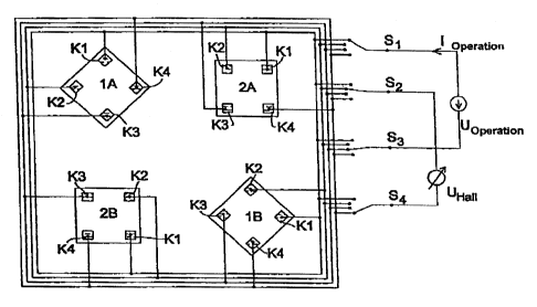
The general structure of a Hall sensor array with two pairs
of Hall sensor elements will now be described making refer-
ence to Fig. 1.
On a semiconductor substrate, which is preferably p-doped,
four rectangular active semiconductor regions are introduced,
these usually being n-doped. Contact electrodes Kl, K2, K3,
K4, which are generally obtained by n+-doping, are preferably
arranged in the corners of the n-doped active region. The
contact electrodes Kl, K2, K3, K4 in the n-doped active re-
gion are arranged diagonally opposite each other in pairs,
two contact electrodes I{1, K3 serving to feed in the operat-
ing current and the other two contact electrodes K2, K4 to
tap off the Hall voltage. The active regions constitute the
individual Hall sensor elements 1A, 2A, 1B, 2B. In the Hall
sensor array with four Hall sensor elements shown in Fig. 1
the Hall sensor elements lA, 1B and the Hall sensor elements
2A, 2B respectively constitute a Hall sensor element pair.
Fig. 1 s.hows an embodiment in which the two Hall sensor ele-
ment pairs are positioned in a square, the individual pairs
of Hall sensor elements being arranged diagonally. However,
the two Hall sensor elements of a pair in the Hall sensor ar-
ray can also be positioned one below the other or next to
each other.
In a preferred embodiment of the Hall sensor array according
to the present invention the contact electrodes KI, the con-
tact electrodes K2, the contact electrodes K3 and the contact
pCT application including amendments annexed to xQER
.
CA 02384583 2002-03-08
- 7 --
electrodes K4 of the individual Hall sensor elements 1A, 2A,
1B, 2B are respectively connected in a parallel arrangement
and are wired together without intermediate switches. in the
representation shown the contact electrodes K1 and the con-
tact electrodes K3 of the Hall sensor elements lA, 2,A, 1B, 2B
constitute the current feed contacts while the contact elec-
trodes K2 and the contact electrodes K4 of the Hall sensor
elements 1A, 2A, 1B, 25 provide the measu.rement terminals for
measuring a Hall voltage. The contact electrodes for feeding
in an operating current and the contact electrodes for meas-
uring a Hall voltage are so arranged in the individual Hall
sensor elements that the current direction of the impressed
operating current is in each case perpendicular to the direc-
tion of the tapped Hall voltage.
In the present invention the operating current directions in
the two Hall sensor elements of each pair are oriented at 90
to each other. The current directions of the second Hall sen-
sor element pair are offset at an angle of 45 to the current
directions of the first Hall sensor element pair.
In the practical implementation of the Hall sensor array ac-
cording to the present invention the angle at which the
operating current directions in the two Hall sensor elements
of each pair are oriented to one another can deviate from the
ideal value of 90 and lie in a range of e.g. 80 to 100 ,
angles in this range being regarded as angles of essentially
90 in the sense of the present invention. This applies also
to the angle by which the current directions of the second
Hall sensor element pair are offset relative to the current
directions of the firat Hall sensor element pair, which can
be chosen to be e.g. in the range 40 to 50 and thus effec-
tively equal to 45 . it should be noted, however, that the
PCT application including amencimenta annexed to XPER
a
CA 02384583 2002-03-08
- $ -
offset compensation of the Hall sensor array which is
achieved may decrease with increasing deviation from the
ideal angles considered as optimal, namely 900 and 45 .
The rigidly interwired contact electrodes Kl, K2, K3, K4 of
the Hall sensor elements 1A, 2A, 1B, 2B are connected to
switches Sl, S2, S3, S4, each of which can be switched be-
tween four positions, i.e. between the contact electrodes Kl,
K2, K3, K4. With the switches S1, 32, S3, S4 the contact
electrodes K1, TG2, K3, K4 can respectively be switched over
together to act as power supply terminals for supplying an
operating current Zoperation or as measurement terminals for
measuring a Hall voltage Uxa11 _
A further embodiment of the Hall sensor array according to
the present invention (not shown explicitly) can provide more
than two pairs of Hall sensor elements. In this case, too,
the operating current directions in the two Hall sensor ele-
ments of each pair are oriented substantially at 90 to each
other. Here, too, the two Hall sensor elements of each pair
must be geometrically the same and be close to one another
relative to the dimensions of the Hall sensor elements and
they can be arranged one under the other, next to each other
or along a diagonal in the complete sensor array. The current
directions of the two or more Hall sensor element pairs are
respectively oriented at an angle of essentially 90 /n to one
another, n being the total number of Hall sensor element
pairs which are used and n 2 2. For example, if three Hall
sensor element pairs are used, the current directions of the
individual Hall sensor element pairs are offset at an angle
of approx. 30 to each other. The element pairs of the sensor
array are arranged either next to each other or along the di-
PCT application including amendments annexed to IPER
s
CA 02384583 2002-03-08
- g ~
agonal, the pairs of Hall sensor elements being as close to
one another as possible.
In this arrangement, too, the contact electrodes for supply-
ing an operating current IopCtation (or a supply voltage) and
also the contact electr4des for tapping the Hall voltage UHa11
are connected in a parallel arrangement and rigidly wired to-
gether without intervening switches.
Through the Hall sensor array with two pairs of Hall sensor
elements, see Fig. 1, or with several pairs of Hall sensor
elements accoxding to the present invention the geometric
placing of the Hall sensor elements already results in a pre-
compensated offset signal in each measurernent phase. This
15, means e.g. that a subsequent amplifier can be operated with
higher amplification since it cannot so easily become satu-
rated. Through the cyclic changeover (e.g. spinning current
operation) of the operating current directions and a suitable
correctly signed and weighted summation or subtraction of the
signals of the individual measurement phases, the precompen-
sated sensor signal offset contribution which still remains
in the individual measurement phases during spinning current
operation is reduced further since the sensor signal offset
contributions due to inhomogeneities and stresses in the
semiconductor material are substantially eliminated.
The specified geometric arrangement of the sensors is advan-
tageous here since the offset contribution of a single Hall
sensor element with only four terminals is smaller than that
of a Hall sensor element with a different geometry, e.g. with
eight contact electrodes. The resulting offset contribution
which remains after cyclic changeover and weighting is there-
fore also smaller. With its geometric arrangement for the
PCT application inc].uding amendIeents annexed to IPER
s
CA 02384583 2002-03-08
- 10 -
Hall sensor array and employing the spinning current method
the arrangement according to the present invention provides a
Hall voltage with an extremely small offset contribution.
This Hall voltage is also independent of the crystal direc-
tion used in the Hall sensor array manufacturing process and
of the orientation of the Hall sensor elements to this crys-
tal direction_
The Hall sensor array is usually implemented as a monolithic
integrated component, which can also accommodate not only the
Hall sensor array but also a current supply for the Hall sen-
sor elements as well as an electronic evaluation circuit for
the Hall voltage. Traditional silicon semiconductor technol-
ogy employing known bipolar or MOS manufacturing processes
generally provides the basis for manufacturing this circuit
arrangement. With the arrangement according to the present
invention the known disadvantages of silicon as a Hall sensor
element material, i.e. a low Hall sensitivity and the big in--
fluence of the piezo effect, which leads to the sensor signal
offset contribution, and also the influence of :lnhomogenei-
ties in the semiconductor material, can substantially be
overcome.
With the parallel connection of the respective contact elec-
trodes Kl, K2, K3, K4 of the individual Hall sensor elements,
which has been described above, only four output terminals
are provided in the Hall sensor array treated here. With
relatively simple circuitry it is possible to switch between
these from one measurement phase to the next and to connect
them to the evaluation electronics. With this fixed wiring it
is possible not only to achieve the advantages as regards
offset compensation described above but also to keep the cir-
cuitry simple, thus making possible a simpler and therefore
PCT application i.nclud3.ng amendments annexed to IPER
a
CA 02384583 2002-03-08
~ - 11 -
cheaper fabrication of these Hall sensor arrays compared with
traditional Hall sensors.
To clarify the concept according to the present invention
some examples of other alternative arrangements of the Hall
sensor elements according to the present invention are de-
sczibed below. It should be noted that the Hall sensor ele-
ments of a pair must be geometrically identical to each
other, whereas, on the other hand, the Hall sensor elements
of different pairs may have different geometries. Thus addi-
tional optimization can be achieved for individual applica-
tions or areas of application of the Hall sensor array.
In Fig. 2a the Hall sensor element pairs lA, 1H and 2A, 2B
are respectively arranged next to one another and the Hall
sensor elements of both pairs have the same geometric form.
In Fig. 2b the Hall sensor element pairs 1A, 1S and 2A, 2B
are respectively arranged next to one another and the Hall
sensor elements of both pairs have different geometric forms.
In Fig. 2c the Hall sensor element pairs 1A, 1B and 2A, 2H
are respectively arranged diagonally and the Hall sensor ele-
ments of both pairs have different geometric forms.
A further advantageous possibility for the geometric arrange-
ment of the individual Hall sensor element pairs is to place
the Hall sensor elements so that the midpoints of the indi-
vidual Hall sensor elements lie on a circle.
An example of the geometric arrangement for two pairs of Hall
sensor elements 1A, 1B and 2A, 2B is shown in Fig. 3a. Con-
necting lines L1, L2 represent the imaginary connection be-
PCT application including amendments annexed to IPER
s
CA 02384583 2002-03-08
- 12 -
tween the geometric midpoints of the two Hall sensor elements
of a pair. The connecting lines Li, L2 of the two pairs of
Hall sensor elements 1A, 1B and 2A, 28 intersect at a point
M, which represents the geometric midpoint of the whole Hall
sensor array. In this geometric arrangement the midpoints of
the individual Hall sensor elements 1A, ].B and 2A, 2B lie
symmetrically on an imaginary circle U with midpoint M.
Fig. 3b shows an example of a geometric arrangement for three
pairs of Hall sensor elements. Connecting lines Ll, L2, L3
represent the imaginary connection between the geometric mid-
points of the two Hall sensor elements of a pair. The con-
necting lines Li, L2, L3 of the three pairs of Hall sensor
elements lA, 18, 2A, 2B, 3A, 3B intersect at a point M, which
represents the geometric midpoint of the whole Hall sensor
array. Xn this geometric arrangement the midpoints of the in-
dividual Hall sensor elements 1A, 1B, 2A, 28, 3A, 3B lie sym-
metrically on an imaginary circle U with midpoint M.
All the Hall sensor arrays described above provide the advan-
tages as regards simplified circuitry demands and improved
offset properties described herein.
PCT application including amendments annexed to IPER