Note: Descriptions are shown in the official language in which they were submitted.
CA 02385031 2002-03-14
WO 01/20664 PCT/SE00/01690
1
A SELF-ALIGNED METHOD FOR FORMING DEEP TRENCHES IN SHALLOW TRENCHES FOR
ISOLATION
OF SEMICONDUCTOR DEVICES
TECHNICAL, FIELD OF THE INVENTION
The present invention generally relates to the isolation of
semiconductor devices in integrated circuits by using isolation
structures, thus enabling increase of the packing density and
isolation.
More specifically, the invention relates to a method for
fabrication of a semiconductor structure comprising a shallow
isolation region and a deep trench isolation region, to the
i0 semiconductor structure itself, and to an integrated circuit
comprising such a semiconductor structure.
DESCRIPTION OF RELATED ART
All non-trivial integrated electronics involves connecting
isolated devices through specific electrical connection paths.
The device isolation scheme is therefore one of the critical
parts when fabricating integrated circuits. Many different
schemes have been developed during the years. Parameters like
minimum isolation spacing, surface planarity, defect density,
process complexity and electrical properties, i.e. DC and high
frequency properties, influence the choice of a scheme for the
particular application and process technology. Mesa isolation,
junction isolation and LOCOS (local oxidation of silicon)
isolation are common techniques in use, see e. g. Chapter 2 in
S. Wolf, "Silicon Processing for the VLSI ERA, Volume 2
Process integration", Lattice Press, Sunset Beach, 1990.
As feature sizes in modern, high-complexity integrated circuits
(ULSI, ultra large scale integration) decreases, there is a
need to reduce shortcomings, such as packing density, leakage
currents and latch-up between devices, associated with older
isolation technologies. Shallow and deep trench isolations have
therefore become very popular. Although demanding on the
CA 02385031 2002-03-14
WO 01/20664 PCT/SE00/01690
2
etching and refilling process steps, they offer vast
improvement in decreased area needed for the isolation between
circuit elements and e.g. storage capacitors in DRAM memory
technologies.
The trenches are formed by removing silicon by dry etching and
filling them with suitable dielectric or conductive materials.
Shallow trench isolation (STI), which is used to replace LOCOS
isolation, usually has a depth of a few tenths of a micron and
is used for isolation between device elements. Shallow trench
isolation is closer described in e.g. "Choices and Challenges
for Shallow Trench Isolation", Semiconductor International,
April 1999, p. 69. Deep trenches, usually with a depth larger
than a couple of microns, are mainly used to isolate different
devices and device groups (wells) in CMOS/BiCMOS technology, to
form vertical capacitors and to form high-conductive contacts
to the substrate, see C. Y. Chang and S. M. Sze (Eds); "ULSI
Technology", McGraw-Hill, New York, 1996, pp. 355-357 and WO
97/35344 (inventors: Jarstad and Norstrom). The trenches are
filled with oxide, polysilicon or other materials, and the
surface is planarised, either by dry etching of by chemical
mechanical polishing (CMP).
In U.S. patent 4,994,406 issued to Vasquez and Zoebel is
described a method to form shallow and self-aligned deep
isolation trenches on an integrated circuit. Although the deep
trench are being self-aligned to the edge of the device areas,
the structure uses a polysilicon nitride stack to form device
isolation using LOCOS, with large lateral encroachment, high
temperature budget, and a non-planar surface as a result.
U.S. patent 5,691,232 issued to Bashir discloses a method to
form shallow and deep trench isolation by combining the
formation of the two. First, a shallow trench is formed using a
first mask, and then a deep trench is formed using a second
mask. The whole structure is filled with oxide and planarised.
CA 02385031 2002-03-14
WO 01/20664 PCT/SE00/01690
3
Since the mask for the deep trench must be aligned against the
mask for the shallow trench, less packing density is achieved
and/or leakage current problems will occur when the structure
is scaled. Also, filling of narrow deep trenches usually
requires the use of polysilicon and back etching, not included
in this description.
In U.S. patent 5,895,253 issued to Akram is described a method
to form a deep trench within a shallow trench and how to fill it
with an insulator. The deep trench is self-aligned within the
shallow trench. This is made with only one mask step. After
forming the trench, it is filled in a common way. Although the
patent teaches how to place a deep trench self-aligned within
the shallow trench, the method uses only one mask step, and it
will not be possible to use shallow trenches without any deep
i5 trench. The width of the deep trench is set by the width of the
shallow trench opening and spacer widths. If different shallow
trench openings are used, the etching and filling of the deep
trenches will become difficult or even impossible.
SUN~IARY OF THE INVENTION
It is consequently an object of the present invention to provide
a method in the fabrication of an integrated circuit,
particularly an integrated circuit for radio frequency
applications, for forming shalicw and deep trenches for
isolation of semiconductor devices comprised in said circuit,
while overcoming at least some of the problems associated with
the prior art.
It is a further object of the invention to provide a
fabrication method that permits deep trenches to be placed
inside shallow trench regions, with adjustable distance from
the edge of the shallow trench to the deep trench, still
allowing the formation of shallow trench areas without any deep
trenches inside.
CA 02385031 2002-03-14
WO 01/20664 PCT/SE00/01690
4
It is yet a further object of the invention to provide such a
method having enhanced scalability characteristics enabling an
increased packing density.
It is still a further object of the invention to provide such a
method having increased integration flexibility and which is
compatible with several technologies.
These objects among others are, according to one aspect of the
invention, fulfilled by a method comprising the following steps:
- providing a semiconductor substrate;
- optionally forming a first dielectric layer on said
substrate;
- forming at least one shallow trench in said first dielectric
layer or in said substrate by using a first mask formed on
said first dielectric layer, said shallow trench extending
into said substrate;
- forming a second dielectric layer of a predetermined
thickness, 2x, on the structure obtained subsequent to the
step of forming the at least one shallow trench;
- forming at least one opening in said second dielectric layer
by using a second mask formed on said second dielectric layer
and with an edge of said second mask aligned to an edge of
said shallow trench with a maximum misalignment of half the
predetermined thickness of said second dielectric layer, i.e.
+/- x, said opening extending within the shallow trench to
the bottom thereof, whereby a spacer of a width equal to the
predetermined thickness, 2x, is formed in said shallow trench
and along said edge thereof; and
- forming a deep trench in said opening by using said second
dielectric layer as a hard mask, said deep trench extending
further into said substrate and being self-aligned to said
shallow trench.
CA 02385031 2002-03-14
WO 01/20664 PCT/SE00/01690
Furthermore it is an cbject of the present invention to provide
a semiconductor structure resulting from above said fabrication
method.
According to a second aspect of the present invention there is
5 thus provided a semiconductor structure comprising a
semiconductor substrate; at least one shallow trench extending
vertically into said substrate; a deep trench laterally within
said shallow trench, said deep trench extending vertically
further into said substrate, wherein said deep trench is self-
aligned to said shallow trench with a controlled lateral
distance between an edge of the shallow trench and an edge of
the deep trench, and the lateral extensions of the shallow and
deep trenches, respectively, are independently chosen.
An advantage of the present invention is that the distance
between the deep and shallow trench edges is fixed and
determined by the thickness of the deposited second dielectric
layer, thus easily controllable.
Another advantage of the invention is that the distance between
the deep and shallow trench edges is minimized in order to
obtain an increased packing density of the integrated circuit,
still providing a step between them in order to prevent stress
arising from deep trench processing to interfere with active
areas.
Further advantages and characteristics of the present invention
will be disclosed in the following detailed description of
embodiments.
BRIEF DESCRIPTION OF THE DRAWINGS
The present invention will become more fully understood from the
detailed description of embodiments of the present invention
given hereinbelow and the accompanying Figs. 1-11 which are
CA 02385031 2002-03-14
WO 01/20664 PCT/SE00/01690
6
given by way of illustration only, and thus are not limitative
of the invention.
Figs. 1-3 and 5-8 are highly enlarged cross-sectional views of a
portion of a semiconductor str~~cture during processing according
to the present invention.
Fig. 4 is a view from above ~f a portion of a semiconductor
structure during processing according to the present invention.
Figs. 9-11 are SEM images of gross-sections of a portion of a
semiconductor structure during processing according to the
present invention.
DETAILED DESCRIPTION OF EMBODIMENTS
In the following description, for purposes of explanation and
not limitation, specific de~~ails are set fourth, such as
particular hardware, applications, techniques, etc. in order to
provide a thorough understanding of the present invention.
However, it will be apparent tc one skilled in the art that the
present invention may be practiced in other embodiments that
depart from these specific details. In other instances, detailed
descriptions of well-known methods, protocols, devices, and
circuits are omitted so as not ~o obscure the description of the
present invention with unnecessary details.
Witr reference to Figs. 1-I- an inventive embodiment of a
process sequence, which includes formation of shallow and deep
trenches, filling of the trenches and planarisation, is
described in detail.
Prior to formation of isolation, sub-collectors, wells or any
other device regions may ha-;e been formed in the starting
material. However, at the stage where the present inventive
process is to be started, the surface of a silicon substrate is
clean and any layers on top of the silicon have been removed.
CA 02385031 2002-03-14
WO 01/20664 PCT/SE00/01690
7
With reference to Fig. 1 the formation of a hard mask for a
shallow trench is described. The masking layer for the shallow
trench is formed by oxidizing silicon surface 10 to form a layer
12 of thermal silicon dioxide of typically 100 A thickness.
Next, an approximately 2000 A thick silicon nitride layer 14 is
deposited by chemical vapor deposition (CVD). Other combinations
of thicknesses and/or masking materials are possible.
With reference next to Fig. 2, the formation of a shallow trench
is considered. A photo resist 16 is applied on the nitride layer
14, and is exposed using a first mask, so called moat mask,
which leaves openings were the shallow trench is to be etched.
The etching, which preferably is non-isotropic, is performed by
reactive ion etching (RIE), through the nitride/oxide layers 12,
14 and into the silicon substrate 10 to form a vertical shallow
trench 18. The preferred depth of trench 18 is 0.2-0.7 Vim, or
more typically 0.3-0.6 ~.un, from the silicon surface 10a. The
photo resist 16 is removed subsequent to the etching of shallow
trench 16.
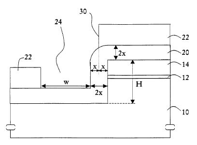
With reference next to Figs. 3 and 4 the formation of a hard
mask for a deep trench is described.
A silicon oxide layer 20 of thickness 2x is deposited,
preferably conformly, e.g. by CVD, on top of the structure,
i.e. remaining portions of the nitride layer 14 and in the
shallow trench 18. It is preferred that the oxide layer 20 is
deposited conformly as otherwise margins for subsequent masking
and etching will be reduced. Photo resist 22 is applied, and is
exposed using a second mask, so called trench mask, which,
together with portion of oxide layer 20, define an opening 24
with a width w for the deep trench.
The layouts of the first and second masks, respectively, are
illustrated in Fig. 4, which shows the semiconductor structure
from above. The edges of the shallow trench and of the opening
CA 02385031 2002-03-14
WO 01/20664 PCT/SE00/01690
8
that will constitute the lateral definition of the deep trench
are indicated by 26 and 28, receptively.
The openings) of the trench mask may be placed anywhere inside
the shallow trench regions. The width of the deep trench can be
chosen by using different mask dimensions. It is usually
preferred to use trenches of fixed lateral dimensions
(thicknesses), preferably of about 1 ~m or less, as problems
otherwise will occur with a non-uniform etch and difficulties
to refill and planarise the deep trench.
One feature of the present invention is the alignment of the
mask edge 30 to the shallow trench edge 20, which makes it
possible to place the deep trench self-aligned with a distance
set by the oxide thickness 2x, which in a preferred example is
between 1000 and 4000 A, and typically 2500 A.
Preferably, the height H of shallow trench 18, oxide layer 12
and nitride layer 14 (i.e. the total etching depth when forming
shallow trench 18) and the thickness 2x of silicon oxide layer
fulfill the following relation:
H > 2x
20 In Figs. 3 and 4 are shown the details of the mask alignment
and the oxide thickness. Assuming that the oxide is 1000
conform (uniform in thickness at steps) with a thickness of 2x,
the trench mask 30 is positioned with an overlap x from the
silicon nitride edge 26, which position was given by the moat
mask. A modern stepper can align the mask with a precision
better, or even much better, than 1000 A.
Next with reference to Fig. 5 the formation of an oxide spacer
32, is considered. The oxide layer 20 is etched by reactive-ion
etching (RIE) to define the trench opening 33 extending to the
bottom surface 18a of the shallow trench. Simultaneously,
sidewall oxide spacer 32 at the shallow trench edge is formed
CA 02385031 2002-03-14
WO 01/20664 PCT/SE00/01690
9
of portion of layer 20, which has a width of 2x. By controlling
she oxide thickness 2x, the distance from the shallow trench
edge to the deep trench opening can be adjusted. On top of the
nitride layer 14, the oxide layer 20 is protected by the photo
resist mask, and this oxide will later serve as a hard mask for
these areas during the following etch step. The oxide layer 20
also is retained at portions of the shallow trench area, where
~:o deep trenches will be formed. After etching the photo resist
is removed.
'rlith reference next to Fig. 6, a deep trench 34 is formed by
etching, using the oxide layer 20 and the spacer 32 as a hard
~~ask. The oxide spacer 32 of ~.aidth 2x defines the distance from
deep trench 34 to the active area. The depth of the deep trench
is at least a few microns, and more preferably at least 5
microns.
:-kith reference now to Fig. 7, the oxide hard mask 20, 32 for the
patterning of the deep trench 32 is removed in e.g. HF.
Subsequent filling and planarisation of trench areas can be
accomplished in several ways known from the literature. As an
_llustrative example, the processing is continued by performing
a liner oxidation, which purpose is to perform corner rounding
at the sharp edge of the trenches, in order to reduce stress
and unwanted electrical effects. This is accomplished by
Growing a thin (200-300 A) thermal oxide 36 at high temperature
(>1000 °C). Since the spacer has been removed, a small "bird's
beak" 38 will be formed in the oxide layer 12 under the nitride
layer 14, which will further add to the corner rounding, see
Fig 7.
Next, with reference to Fig. 8, the trench is filled in a
conventional manner with a 2000 A thick layer 38 of TEOS and
with 15000 A of polysilicon 40. The polysilicon is then etched
back to remove all polysilicon from the shallow trench areas.
CA 02385031 2002-03-14
WO 01/20664 PCT/SE00/01690
Alternatively, the polysilicon is planarised by chemical
mechanical polishing before the polysilicon is etched back from
the shallow trench areas. Hereby, the recess of the polysilicon
5 fill in the deep trench is reduced. Consequently, a thinner
oxide can be deposited in the subsequent step to fill the
shallow trench.
Alternatively, a dielectric is used to fill the trenches
instead of polysilicon. Finally, the remaining shallow trench
10 is filled with e.g. CVD oxide 42 or a high density plasma (HDP)
oxide, and planarised, either by dry etching methods or by
chemical mechanical polishing. The resulting structure is shown
in Fig. 8. The processing continues further with forming of the
active devices etc., which is not shown in the Figures, and
will not be further described in this description.
With reference next to Figs. 9-11, SEM (scanning electron
microscope) images of cross-sections of a portion of the
semiconductor structure during processing according to the
present invention will be briefly discussed.
Structures as obtained prior to trench filling are shown in
Figs. 9 and 10. Note that the oxide/nitride layers on top are
not distinctly visible. In Fig. 9 the scanning electron
micrograph shows shallow trench areas without any deep trench
(left-most and right-most structures) and another shallow trench
area with two deep trenches self-aligned to the edges of the
shallow trench area (in the middle). The framed area indicated
by 44 corresponds to the structure shown in Figs. 1-3 and 5. In
Fig. 10 the micrograph shows device areas 46 for two bipolar
transistors 48, 50 as indicated in the Figure, where the deep
trench close to the collector contact area 52 is self-aligned to
the shallow trench isolation edge.
CA 02385031 2002-03-14
WO 01/20664 PCT/SE00/01690
11
Finally, Fig. 11 shows a SEM image of the structure subsequent
to the back etching when the polysilicon is removed from the
shallow trench areas. In the Figure the structures resulting
from the etching are indicated by 54 and the 2000 A thick TEOS
layer on top of the nitride/oxide layers and in the trench
areas is indicated by 56.
In summary, the present invention uses an additional mask
(trench mask) step and makes it compatible with shallow trench
isolation, to create a planar surface. Deep trenches may be
placed anywhere within shallow trench areas. Furthermore, by
forming an oxide spacer at the shallow trench step, the deep
trench can be formed self-aligned to the shallow trench. The
distance from the deep trench to the active area is controlled
by the hard mask oxide thickness. This maximizes packing
density and prevents the trench from reaching active areas,
which may lead to leakage currents, reduced breakdown voltage
or other unwanted effects.
Thus, the present invention exhibits i.a. following advantages:
- The STI overlap between deep trench and active device areas
(i.e. distance between deep trench edge and shallow trench
edge, 2x) is minimized and easily controllable.
- The separation of the deep trench from active areas
determined by the STI edge is self-aligned and prevents
stress arising from deep trench processing to interfere with
active areas.
- The separation is determined by deep trench hard mask
thickness (and possibly combined with STI stack height, i.e.
depth of shallow trench).
- The trench localization is fixed and determined by the
additional mask (trench mask).
CA 02385031 2002-03-14
WO 01/20664 PCT/SE00/01690
12
- The additional mask is positioned on oxide spacer created for
hard mask definition to accommodate for any misalignment
(spacer width 2x gives an allowable misalignment of +/- x)
- Removal of oxide spacer of ter deep trench etch to allow for
simultaneous corner rounding of deep trench and STI close to
active area (bird's beak).
It will be obvious that the invention may be varied in a
plurality of ways . Such variations are not to be regarded as a
departure from the scope of the invention. All such
modifications as would be obvious to one skilled in the art are
intended to be included within the scope of the appended claims.