Note: Descriptions are shown in the official language in which they were submitted.
CA 02385084 2002-03-14
1
DESCRIPTION
LIGHT-RECEIVING ELEMENT AND PHOTODETECTOR USING THE SAME
TECHNICAL FIELD
The present invention relates to a light-receiving
element for continuously detecting a light intensity and a
barycenter thereof for the spectrum of a long-wavelength band
(e. g., 1.3-1.55,ctm band) used in an optical communication
field, a photodetector employing such a light-receiving
element, and an optical demultiplexer using such a
photodetector.
BACKGROUND ART
An optical demultiplexer (for example, Light Detecting
System PSS-100 commercially available by Shimazu Seisakusho)
has been known in which the light collected by a collective
lens is reflected by a mirror, the reflected light is
demultiplexed by a dittraction grating, and the demultiplexed
lights are detected by a photodetector. The photodetector
employed in this optical demultiplexer is a light-receiving
element array and is used as a spectrum monitor for
wavelength.
In this conventional photodetector, the barycenter of a
light intensity is monitored by dividing the spectrum of one
wavelength by means of an array of light-receiving elements
(e.g., five elements). Therefore, the resolution of the
photodetector is determined by an array pitch of the light
receiving elements. In this manner, the conventional
photodetector may merely obtain the resolution corresponding
CA 02385084 2002-03-14
2
to the array pitch of the light-receiving elements, so that
it is difficult for the conventional photodetector to further
increase its resolution. It should be noted that the
barycenter of a light intensity means herein the barycenter
of spectrum distribution of a wavelength.
In order to resolve the problems described above, the
inventors of this application have thought that a
semiconductor position sensor for detecting the position of a
light spot is used as a light-receiving element array of the
photodetector in the optical demultiplexer. Because the
semiconductor position sensor is a non-divided type of
element different from the light-receiving element array
described above, the semiconductor position sensor may detect
continuously and spatially the barycenter of a light
intensity.
As a conventional semiconductor position sensor, the
sensor has been known in which a p-type resistor layer is
provided on the top surface of a high-resistance Si substrate
(i-type layer), on the bottom surface thereof a n-type layer
is provided, and two electrodes are provided oppositely on
the p-type resistor layer.
Because surface layers form a p-n junction in this
semiconductor position sensor, a photocurrent is generated
due to a photoelectric effect when an incident light impinges
upon the p-type resistor layer. The photocurrent generated
at the position upon which an incident light impinges is
divided into two currents, respective magnitude thereof being
in reverse proportion to respective resistances from the
light impinging position to respective two electrodes, so
that the light impinging position may be detected by
CA 02385084 2002-03-14
3
monitoring each current derived from respective two
electrodes.
The conventional semiconductor position sensor uses a Si
substrate as described above, and then has a poor sensitivity
in a long-wavelength band for an optical communication.
Therefore, in a case that the conventional semiconductor
position sensor is used for a light-receiving element array
of an optical demultiplexer, it is difficult to detect the
barycenter of a light intensity of light having a long
wavelength band.
DISCLOSURE OF THE INVENTION
An object of the present invention is to provide a
light-receiving element used in a photodetector of an optical
demultiplexer, which may detect the barycenter of a light
intensity of light including a long-wavelength band.
Another object of the present invention is to provide a
photodetector of an optical demultiplexer , which uses such a
light-receiving element.
A further object of the present invention is to provide
an optical demultiplexer having an increased resolution using
such a photodetector.
According to the present invention, a semiconductor
position sensor using III-V group compound semiconductor
having a good sensitivity in a long-wavelength band (e. g.,
1.55,u m band) for an optical communication is used as a
light-receiving element in order to monitor the spectrum of
the long-wavelength band.
A first aspect of the present invention is a light-
receiving element for detecting a light intensity and a
CA 02385084 2002-03-14
4
barycenter thereof for an incident light of a long-wavelength,
the light-receiving element comprising a semiconductor layer
of III-V group compound semiconductor ; a first conductivity-
type of resistor layer provided on the top surface of the
semiconductor layer ; a second conductivity-type, opposite to
the first conductivity-type, of substrate provided on the
bottom surface of the semiconductor layer ; and at least one
pair of opposing electrodes provided on the resistor layer.
A second aspect of the present invention is a
photodetector for detecting a light intensity and a
barycenter thereof for each of lights demultiplexed from an
incident light, the incident light including a plurality of
wavelengths, the photodetector comprising one or more light-
receiving elements described above.
A third aspect of the present invention is an optical
demultiplexer for demultiplexing an incident light including
multiplexed wavelengths, the optical demultiplexer comprising
an optical means for demultiplexing the incident light into a
plurality of lights ; and a photodetector for receiving the
plurality of light demultiplexed by the optical means. An
array of light-receiving elements described above may be used
for the photodetector.
BRIEF DESCRIPTION OF THE DRAWINGS
Fig.lA is a plan view of a light-receiving element in
accordance with the present invention,
Fig.lB is a cross-sectional view taken along the X-Y
line in Fig,lA.
Fig.2 is a diagram of a circuit for measuring the
position upon which an incident light impinges using a
CA 02385084 2002-03-14
current from an light-receiving element.
Fig.3 is a diagram of a time-division type of
photodetector.
Fig.4 is a diagram of a photodetector for detecting a
5 light intensity and the barycenter thereof for each of
demultiplexed lights.
Fig.5 is a plan-view of the photodetector shown in Fig.4.
Fig.6 is a diagram of another photodetector for
detecting a light intensity and the barycenter thereof for
each of demultiplexed lights.
Fig.7 is a diagram of an optical demultiplexer in
accordance with the present invention.
Fig.8 is a diagram illustrating the structure for
detecting each barycenter of k, wavelengths of C-band and k2
wavelengths of L-band.
Fig.9 shows an example in which two lines of light-
receiving elements each line having the same number of
elements are integrated in one semiconductor chip.
BEST MODE FOR CARRYING OUT THE INVENTION
First Embodiment
Referring to Figs.lA and 1B, there is shown a light-
receiving element in accordance with the present invention,
i.e. a light-receiving element 8 for monitoring one
wavelength. Fig.lA is a plan view, and Fig.lB is a cross-
sectional view taken along the X-Y line in Fig,lA. In the
light-receiving element 8, an InGaAs layer (i-type layer) 12
and a p-type InP layer 14 are stacked on an n-type InP
substrate 10. Electrodes 16a and 16b are formed on both
sides of the top surface of the p-type layer 14, and an
CA 02385084 2002-03-14
6
electrode (not shown) is formed on the bottom surface of the
n-type substrate 10.
The basic operation of the light-receiving elements 8
will now described. An incident light impinged upon the
light-receiving element is photoelectric-converged into a
photocurrent which flows in the p-type layer 14 toward the
electrodes 16a and 16b. As a result, a current is derived
from each of the electrodes 16a and 16b, the magnitude
thereof being dependent on the distances from the light
impinging position to respective electrodes 16a and 16b.
That is , the photocurrent I is divided into two currents in
reverse proportion to respective resistances from the light
impinging position to respective electrodes 16a and 16b. It
is assumed herein that the distance between the electrodes
16a and 16b is L~,,, and the distance between the light
impinging position and the electrade 16a is L$.
If the sheet resistance of the p-type layer 14 is
uniform, then the currents Ia and Ib derived from the
electrodes 16a and 16b are represented by the following
formulas.
I$ =I X ( Lab -La ) /Lab ( 1 )
Ib =I X L$ /Lab ( 2 )
The ratio of Ia to Ib and the ratio of the subtraction (I$ -
Ib) to the summation (Ia +Ib) are calculated as follows.
Ia /Ib =Lab /La -1 ( 3 )
( Ia -Ib ) / ( Ia +Ib )
=1- ( 2La /L~b ) ( 4 )
It is appreciated that respective ratios of Ia /Ib and
(I$ -Ib )/(Ia +Ib ) are the values irrelevant to a light
intensity and a variation thereof. Therefore, if respective
CA 02385084 2002-03-14
7
ratios of Ia /Ib and ( Ia -Ib ) / ( Ia +Ib ) in the formulas ( 3 ) and
(4) are measured, then the distance L, may be obtained. As a
result, the light impinging position may be precisely
detected irrelevantly to the variation of a light intensity.
In the light-receiving element of the present embodiment,
the material of InGaAs system having a high photo sensitivity
for a long-wavelength is used, so that a high performance
detection of the light impinging position may be possible for
a long-wavelength for which the material of Si system has a
poor sensitivity. As the material of InGaAs system, III-V
group compound semiconductor such as GaAs, AlGaAs, InAs,
InGaAsP, and the like may be used. Also, Ge may be used in
an infrared wavelength. The summation of the currents Ia and
Ib is equal to the photocurrent I, so that the intensity of
an incident light may be monitored from the photocurrent I.
Referring to Fig.2, there is shown a circuit for
measuring the position upon which an incident light impinges
using the current Ia and Ib derived from the electrodes 16a
and 16b of the light-receiving element 8. The currents Ia
and Ib are amplified by preamplifiers 1 and 2, respectively,
and the amplified currents are summed in an adder 3 to obtain
(I$ +Ib ) as well as are substrated in a substracter 5 to
obtain ( Ia -Ib) . Then, the division ( Ia -Ib ) / ( Ia +Ib ) is
calculated in a divider 5 to measure the light impinging
position based on the formula (4).
While the circuit shown in Fig.2 employs a method for
detecting the light impinging position based on the formula
(4), the light impinging position may be measured by
calculating the division Ia /Ib based on the formula (3).
Second Embodiment
CA 02385084 2002-03-14
8
A time-division type of photodetector in accordance with
the present invention will now be described, the
photodetector detecting a light intensity and a barycenter
thereof for each of N lights which are demultiplexed from an
incident light including multiplexed N time-divisioned
wavelength by a diffraction grating.
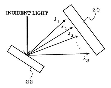
Fig.3 shows a photodetector 20 for monitoring the
demultiplexed N lights of wavelengths ~ 1, ~ 2, ..., ~l N. While
the structure of the photodetector 20 is basically the same
as that of the light-receiving element 8 shown in Fig.l, the
light-receiving area of the photodetector is formed so large
as to receive all the demultiplexed lights. In Fig.3, the
incident light including N time-divisioned wavelength is
demultiplexed into N lights by a diffraction grating 22. The
demultiplexed lights including wavelengths ~l 1, ~ z, .... ~l N,
respectively, impinge upon the photodetector 20.
When each of the demultiplexed lights impinges upon the
photodetector 20, the photodetector may operate in a time-
divisional manner to detect the barycenter of a light
intensity for each of N demultiplexed lights. Also, each
light intensity of N demultiplexed lights may be detected
from respective photocurrents as illustrated with reference
to Fig. 1.
Third Embodiment
A photodetector in accordance with the present invention
will now be described, the photodetector detecting a light
intensity and a barycenter thereof for each of N lights which
are demultiplexed from an incident light including
multiplexed N wavelength by a diffraction grating.
Fig.4 shows a photodetector 30 for monitoring the
CA 02385084 2002-03-14
9
demultiplexed N lights of wavelengths ~l " ~l z. ~.~. ~ N~ The
photodetector 30 is structured by N light-receiving elements
D1, Dz, ..., DN arrayed in one dimension. Each light-receiving
element is a light-receiving element as illustrated with
reference to Fig.l. Fig.S shows a plan-view of the
photodetector 30. Respective light-receiving elements are
arrayed so that the electrodes 16a and 16b of respective
element are lined up in an arraying direction of the elements.
In the present embodiment, the incident light including
N wavelengths is demultiplexed into N lights by a diffraction
grating 22, and the demultiplexed N lights impinge upon N
light-receiving elements, respectively. As a result, the
barycenter of a light intensity of each of N demuitiplexed
lights may be detected. Also, each intensity of N
demultiplexed lights may be detected from a photocurrent of
each light-receiving element as illustrated with reference to
Fig. 1.
Forth Embodiment
Another example of a photodetector in accordance with
the present invention will now be described, the
photodetector detecting a light intensity and a barycenter
thereof for each of N demultiplexed lights which are
demultiplexed from an incident light including multiplexed N
wavelength by a diffraction grating.
Fig.6 is a diagram for illustrating this photodetector.
In this photodetector, an incident light is split into two
lights by a half mirror 40. One split light is demultiplexed
into N lights by a diffraction grating 42, and each
barycenter of the light intensities thereof is detected by a
first photodetector 30 shown in Fig.5. The other split light
CA 02385084 2002-03-14
is demultiplexed into N lights by a dittraction grating 44,
and respective light intensities of N demodulated lights are
detected by a second photodetector 46 consisting of N
photodiodes PD1, PDz, ..., PDN each positioned at the focal
5 point of demultiplexed light.
In this embodiment, the second photodetector 46 may be
fabricated so that the light-receiving area thereof is
smaller than that of the first photodiode 30, resulting in
the reduction of noise therein. As a result, the second
10 photodetector 46 is suitable for detecting the light
intensity of a weak incident light.
Fifth Embodiment
An optical demultiplexer in accordance with the present
invention will now be described, the optical demultiplexer
using the photodetector in the second or third embodiment.
Fig.7 shows an optical demultiplexer in an optical
communication system based on a wavelength multiplexed
transmission, which may be used for demultiplexing a
wavelength multiplexed incident light into a plurality of
lights each having a different wavelength, and for detecting
each light intensity and barycenter thereof for respective
demultiplexed lights. The optical demultiplexer comprises
components such as one input optical fiber 50, a collimator
lens 52, a diffraction grating 54, and an optical detector 56,
which are accommodated in three tubular members fitted to
each other. The input optical fiber 50 is fixedly coupled to
a window 60 for fixing the fiber by means of a fiber coupling
member 62, the window 60 being an end face of a transparent
tube 58 for accommodating the fiber. The collimator lens 52
is fixed to an end of an intermediate tube 64. The
CA 02385084 2002-03-14
11
diffraction grating 54 is fixed to a window 68, the window 68
being an end face of a tube 66 for accommodating the
diffraction grating. In this optical demultiplexer, the
tubes 58 and 66 are fitted to both ends of the intermediate
tube 64 so as to be movable in the direction of light axis
and rotatable around the light axis for active alignment.
According to this optical demultiplexer, the light from
the input optical fiber 50 impinges upon the diffraction
grating 54 via the collimator lens 52. The light is
demultiplexed by the diffraction grating 54, and the
demultiplexed lights pass through the collimator lens 52 to
be detected by the photodetector 56.
The photodetector 56 may detect each light intensity and
a barycenter thereof for respective demultiplexed lights, as
explained in the embodiments 2 and 3.
As in the photodetector illustrated in the embodiment 4,
the structure may be employed in which a wavelength
multiplexed light is split into two lights to detect the
barycenter of a light intensity by the first photodetector 30
and a light intensity by the second photodetector 46.
Sixth Embodiment
Fig.8 shows the case that, in an optical communication
system, an incident light includes k1 wavelengths (k1 is an
integer equal to or larger than 1) of C-band and k2
wavelengths ( k2 is an integer equal to or larger than 1 ) of
L-band, the k1 and k2 wavelengths being multiplexed. The
incident light is demultiplexed into k1 lights of C-band and
k2 lights of L-band by a diffraction grating 70, respectively.
Respective barycenters of the light intensities of (kl+k2)
demultiplexed lights may be detected by a first photodetector
CA 02385084 2002-03-14
12
(not shown) consisting of k1 light-receiving elements for C-
band and a second photodetector (not shown) consisting of k2
light-receiving elements for L-band.
When the first photodetector for C-band and the second
photodetector for L-band are formed on separate semiconductor
chips, respectively, it is difficult that the relative
position and the parallelism between semiconductor chips are
implemented with high accuracy. Therefore, it is preferable
that the first and second photodetectors are integrated in
one chip. If the incident angles of lights of C and L-bands
to the diffraction grating 70 are preferably selected, then
the demultiplexed lights of C and L-bands may be collected on
two adjacent lines. The first and second photodetectors are
arrayed in two lines on the positions upon which the
demultiplexed lights impinge. Herein, the incident light of
C-band impinges upon the diffraction grating at a smaller
angle to the normal of the diffraction grating in comparison
with the incident light of L-band.
The arrangement of light-receiving element in one
semiconductor chip is not limited to a line of k1 elements of
C-band and a line of kZ elements of L-band, but two lines of
elements each line having the same number of elements may be
arranged. For example, two lines of elements each line
having k1 element ( i.e. , k1 elements X 2 lines ) in the case of
kl~ k2 may be provided in one semiconductor chip, or two lines
of elements each line having k2 element (i.e., k2 elementsX2
lines) in the case of k1 ~ k2 may be provided in one
semiconductor chip. Fig.9 shows an example in which two
lines of light-receiving elements 8 each line having the same
number of elements are integrated in one semiconductor chip
CA 02385084 2002-03-14
13
72.
The incident light including two bands, i.e. C-band and
L-band, has been explained hereinbefore. Generally, for the
incident light including k bands, k lines of light-receiving
elements may be arranged in two dimensions to detect the
demultiplexed lights.
The photodetector having described-above structure may
be used for the light demultiplexer shown in Fig.7.