Note: Descriptions are shown in the official language in which they were submitted.
CA 02385364 2002-03-19
WO 01/22542 PCT/DK00/00521
MULTI - WAVELENGTH LASER SYSTEM
The present invention relates to a system and a method providing multi-
wavelength
emitting optical integrated planar waveguide device with large wavelength
span, having
tight control over absolute and especially relative positions of the emitted
wavelengths, as
well as narrow line widths.
Since the onset of interest in the research area known as Integrated Optics,
the aim of
research has been towards fabricating highly functional optical integrated
circuits (OIC's)
with a high level of integration of state-of-the art components.
A vast number of different materials systems and technologies are used for the
fabrication
of these OIC~s. Typically used technologies for OIC's are based either on
glass-, polymer-
or semiconductor materials, each of these technologies having pros and cons.
However,
common to all OIC's is the ability to produce and/or manipulate light signals,
which
typically are launched into an optical fibre either for telecommunication
purposes, test-
measurement- or sensor applications.
Within optical telecommunication, OIC's such as dense wavelength division
multiplexers
(DWDM's) and optical add/drop multiplexers are expected to play an increasing
role in the
future as more and more standard ITU (International Telecommunication Union)
channels
are transmitted through single fibres. The spacing of ITU channels varies when
technology evolves making it possible to have more channels within less
wavelength
span. At the time, standard minimum ITU channel spacing is 100GHz or 50GHz.
These
components perform operations on the transmitted signals that would otherwise
be very
hard to achieve using an all-fibre solution. Furthermore, the OIC's are likely
to be smaller,
cheaper and more stable than bulk optics solutions. Other uses for OIC's
include e.g.
small gyroscopes and electrical field sensors.
For telecommunication-, measurement-, and sensor-applications, the light
sources
typically used are lasers, as these emit at definite wavelengths with narrow
line widths,
making it possible to transmit more standard ITU channels through a fibre, or
to make
more precise measurements. Furthermore, the coherence and phase of the laser
light is
extensively used in as well telecommunication as in several OIC's such as ring
resonators
SUBSTITUTE SHEET (RULE 26)
CA 02385364 2002-03-19
WO 01/22542 PCT/DK00/00521
2
and Mach-Zehnder switches. Thus, there is a promising market for lasers, and
especially
multi-wavelength lasers.
To fully exploit the transmission possibilities of the fibres and the OIC's, a
conglomerate of
individual lasers each emitting at a specific wavelength is required, which
will be an
expensive as well as a bulky solution. Therefore, an integrated optical device
emitting at
multiple definite wavelengths that can be individually modulated is likely to
be highly
attractive as light source in high bit-rate DWDM networks. For testing of
OIC's for DWDM
networks, and the networks themselves a simple integrated optical device
without
modulators emitting at a range of wavelengths on the ITU communication grid
will prove
to be very useful.
Such multi-wavelength emitting laser devices need to possess certain qualities
for them to
qualify as sources in the above-mentioned applications, such as temperature-
and
channel stability, narrow line widths as well as single-mode and single
polarisation
operation.
Besides these qualities it will be advantageous if the multi-wavelength
emitting devices
can be fabricated in a technology, which facilitates good interfacing to the
optical fibres.
Matching the fibre and the device material systems ensures optimal coupling of
the optical
signal from the device to the fibre and vice versa.
Multi-wavelength emitting devices have been fabricated in the past, in a
number of
different technologies.
One way to come about such a device is by splicing together a number of
separate fibre
lasers, each emitting at a predetermined wavelength. Such a solution
facilitates excellent
coupling of light from the laser structure to fibre networks. Furthermore,
this method
provides easy amplification of the laser signals around 1550 nm by using the
non-
absorbed pump light to pump an erbium doped fibre amplifier in conjunction
with the
lasers.
J. Hubner et al. "Five wavelength DFB fibre laser source for WDM systems",
Electronics
Letters, Vol. 33, No. 2, January 1997, pp. 139 - 140, discloses a five
wavelength fibre
laser source. The disclosed method consists of fabricating five separate
lasers in erbium
SUBSTITUTE SHEET (RULE 26)
CA 02385364 2002-03-19
WO 01/22542 PCT/DK00/00521
3
doped fibres, and subsequently splicing together the separate fibre lasers
into one multi-
wavelength emitting device. The individual lasers show a peak power of 150 NW
and a
line width of less than 15 kHz when pumped by 60 mW of 1480 nm light. Using
this
approach, the authors achieved polarisation and longitudinal single mode
operation of the
lasers.
Using UV-exposure and a single phasemask to inscribe the Bragg gratings into
the cores
of the fibres, J. Hubner et al. achieved varying Bragg laser wavelengths by
applying stress
to the fibres during Bragg grating fabrication. When no stress is applied to
the fibre during
grating inscription, the resulting Bragg wavelength is given by the phasemask
period
(assuming the laser is operated without applied stress). On the other hand, if
the fibre is
stretched during grating inscription the effective inscribed grating period
will decrease
when the stress is released, hence decreasing the wavelength at which the
grating will
reflect. This technique allows the authors a tuning range of approximately 5
nm, with a
reproducibility of around 0.2 nm.
Multi-wavelength emitting devices can also be fabricated in semiconductor
materials,
where passive and active sections can be made, making it possible to form
passive
waveguides as well as lasers in the active regions. Distributed feedback (DFB)
lasers can
be formed in the active regions, with direct injection into passive
waveguides. Tailoring the
passive waveguide structure to multiplex the signals from the separate lasers
into a single
waveguide facilitates easy coupling of the output wavelengths into a fibre.
Modulation of
the laser outputs becomes very easy as the lasers are modulated by the current
sources.
Furthermore, due to the high refractive index contrast typically experienced
in such
semiconductor structures the size of such a structure can be made particularly
small.
K. Aiki et al. "Frequency multiplexing light source with monolithically
integrated distributed-
feedback diode lasers", Appl. Phys. Lett., Vol. 29, No. 8, October 1976, pp.
506 - 508,
discloses a method of fabricating an array of six GaAs-GaAIAs DFB diode
lasers,
multiplexed into one output waveguide. Liquid-phase epitaxy (LPE) was used to
successively grow differently doped layers, forming an active sandwich
structure where
the lasers were to be fabricated. Six third order gratings with varying period
were
subsequently made one at a time on the surface, using a holographic exposure
setup with
a sliding slit, and subsequent chemical etching. Following the grating
formation, all except
the grating regions were completely etched away down to the substrate, and
passive
SUBSTITUTE SHEET (RULE 26)
CA 02385364 2002-03-19
WO 01/22542 PCT/DK00/00521
4
GaAIAs layers were regrown using LPE, followed by the formation of a passive
waveguide
structure, multiplexing the separate laser outputs into one waveguide.
This fabrication method allowed the authors to obtain a laser wavelength
separation of 2
nm ~ 0.5 nm around approximately 864 nm, and a spectral width of the lasers of
approximately 0.03 nm. Due to the abrupt transition from the lasers to the
passive
waveguides a very low coupling efficiency of approximately 30% was obtained,
contributing to an over-all quantum efficiency as measured at the terminal of
approximately 0.3%.
In order to reduce the coupling loss and back reflection from the interface
between a
multi-wavelength emitting device and fibre the multi-wavelength emitting
device should be
made in a fibre compatible material regarding refractive index, e.g., silica.
Furthermore,
the refractive index profile of the waveguides and hence the mode profile
should be fibre
compatible.
D. L. Veasey et al. "Arrays of distributed-Bragg-reflector waveguide lasers at
1536 nm in
Yb/Er codoped phosphate glass", Appl. Phys. Lett., Vol. 74, No. 6, February
1999, pp.
789 - 791, discloses a method of fabricating an array of integrated waveguide
lasers in a
phosphate glass substrate. The waveguides were formed by K+/Na' ion exchange
in an
Erbium/Ytterbium co-doped phosphate glass, using 3 - 8 Nm wide line apertures.
The
DBR structure was formed using a thin highly reflective dielectric mirror on
the pump input
facet, and a surface relief Bragg grating in the other end. This Bragg grating
is initially
formed in a thin layer of photoresist using a holographic exposure setup, and
development. Covering the top of the developed photoresist structure with
chromium, the
photoresist structure is transformed into the surface of the waveguides using
reactive ion
etching.
This approach allowed the authors to obtain lasers with stable longitudinal
single mode
operation, line widths less than 500 kHz, and output powers of 80 mW. By
varying the
aperture widths from 5 Nm to 8 Nm and measuring the position of the
corresponding laser
wavelengths it was found that the wavelength span ranged from approximately
1536.0 nm
at 5 Nm width, to approximately 1536.3 nm at 8 Nm width. The wavelength span
of
approximately 0.3 nm over 3 p.m of wavelength width, corresponds to less than
50 GHz,
which compares to the spacing between two adjacent ITU channels.
SUBSTITUTE SHEET (RULE 26)
CA 02385364 2002-03-19
WO 01/22542 PCT/DK00/00521
Kitagawa et al. "Single frequency Er3+-doped silica-based planar waveguide
laser with
integrated photo-imprinted Bragg reflectors", Electronic Letters, Vol 30, No.
16, pp. 1311
- 1312, August 1994, relates to two identical planar waveguide lasers, formed
in doped
5 silica glass. The lasers are formed by making waveguide cores of Er3+-doped
silica,
embedded in silica claddings. The waveguide cores has dimensions 8 x 7 p.m and
are
formed using standard deposition and etching techniques. Using UV writing
through a
phase mask, two spatially separated Bragg gratings are induced in the core,
forming a
DBR laser cavity. Single frequency (or mode) operation with an output of 340
p.W is
obtained at 1546 nm, for pump powers less than 300 mW. The presented lasers
emit at
the same single wavelength and do therefore not apply as a multi-wavelength
emitting
device source for IOC uses. The reference contains no possibilities for
varying the laser
wavelength of the lasers. Moreover, the geometrical parameters of the
waveguide are
considered unfavourable. An 8 x 7 pm cross section area will typically support
several
transverse modes.
Single mode waveguides are required in order to obtain efficient transmission
in
waveguides and fibres, as well as good coupling from waveguides to fibres.
Also, the
combination of the waveguide cross section dimensions and the refractive index
step
should be optimised to ensure optimum mode overlap between the signal mode at
15xx
nm (28 <_ xx <_ 68), and the pump mode at 980 nm, alternatively 1480 nm. This
helps
optimising gain in the active medium.
Having a multi-wavelength emitting device formed as a series of spliced DFB
fibre lasers
is disadvantageous, since an isolator is often needed in between each of the
lasers, thus
increasing cost and complexity. Furthermore, the number of cascaded lasers is
limited by
the requirement of uniform output power at the different laser wavelengths.
Due to pump
power absorption in the lasers and the isolators, the output power from the
lasers further
down the line will decrease, ultimately limiting the number of lasers to a
maximum of
approximately eight lasers.
It is another disadvantage of multi-wavelength emitting device formed as a
series of
spliced DFB fibre lasers, that each laser is fabricated individually. This
introduces some
uncertainties in the relative laser frequencies of a series of lasers.
SUBSTITUTE SHEET (RULE 26)
CA 02385364 2002-03-19
WO 01/22542 PCT/DK00/00521
6
It is a disadvantage of multi-wavelength emitting devices formed in
semiconductor
materials that the index of refraction of these materials is much higher than
the refractive
index of silica fibres, giving rise to very high coupling losses as well as
back reflections,
which might disturb the stability of the lasers.
The method of using phosphate glass for multi-wavelength emitting devices
poses a
number of disadvantages:
While the refractive index of a typical phosphate glass is considerably
smaller than that of
semiconductor materials, it is still somewhat larger than that of standard
silica fibres, thus
giving rise to coupling loss and back reflections which also might disturb the
stability of the
lasers.
There is a reduction of the wavelength span originating from the phosphate
glass host,
which effectively prevents amplification above approximately 1544 nm. This low
upper-
limit for amplification excludes a very large range of ITU channels, thereby
significantly
limiting the applicability of such devices.
Furthermore, the only possibility of varying the laser wavelengths
considerably in order to
cover a large span of ITU channels is to vary the physical grating period,
which increases
the complexity and cost of the device.
In the device of D. L. Veasey et al., the very small span of approximately 0.3
nm is most
likely due to the nature of the graded refractive index profile obtained in
the ion exchange
process.
Another disadvantage of the device of D. L. Veasey et al. is, that DBR lasers,
fabricated
using the presented method are prone to be easily affected by external
influences, as the
grating and the waveguides are directly accessible on the upper surface of the
device.
SUMMARY OF THE INVENTION
It is an object of the present invention to provide a multi-wavelength
emitting laser device
wherein it is possible to span several standard ITU channels by varying the
transverse
dimensions of waveguides having the same grating period.
SUBSTITUTE SHEET (RULE 26)
CA 02385364 2002-03-19
WO 01/22542 PCT/DK00/00521
7
It is another object of the present invention to provide a multi-wavelength
emitting laser
device where Bragg gratings can be imprinted with a single exposure session
using
coherent actinic radiation. Thus, Bragg gratings can be made simultaneously in
several
waveguide cores, which gives a high degree of precision, making it possible to
precisely
control the position of the emitted wavelengths.
It is a further object of the present invention to provide a multi-wavelength
emitting laser
device in which the Bragg gratings are UV written. This allows for a fine-
tuning of the
emitted wavelengths in a post-processing step using a focused beam of actinic
radiation
and scanning the previously fabricated Bragg gratings.
It is a still further object of the present invention to provide a multi-
wavelength emitting
laser device where the macroscopic variations in the silica layers across the
substrate,
and macroscopic variations in the photolithography and etching steps, can be
neglected
since the lasers are placed in close proximity.
It is a still further object of the present invention to provide a multi-
wavelength emitting
laser device that eliminates local temperature fluctuations from external
influences by
employing silicon as a substrate, which has thermal conductivity two orders of
magnitude
larger than silica. This ensures consistent laser channel spacing.
It is a still further object of the present invention to provide a multi-
wavelength emitting
laser device having a high mechanical stability, achieved by the high out-of-
plane bending
stiffness property of the silicon substrate.
According to the present invention, the above-mentioned objects are complied
with by
providing waveguide lasers having a well-defined refractive index profile. At
any cross
section of the laser cavity, the overlap between the index profile and a
transverse mode of
a laser mode at least partly determines the effective refractive index neft
experienced by
the laser mode. The index profile is typically determined by the shape of the
waveguide
core surrounded by a cladding. Hence, according to the present invention, by
providing a
well-defined index profile, a change in one of the transverse dimensions of
the waveguide
core will give rise to a large change in the overlap between the index profile
and a
transverse mode of the radiation. Thus, the variation of the transverse
dimensions of the
waveguide core translates directly into a substantial variation of the
effective refractive
SUBSTITUTE SHEET (RULE 26)
CA 02385364 2002-03-19
WO 01/22542 PCT/DK00/00521
8
index, neff, as experienced by laser modes of interest. Throughout the present
description
and claims, the cross-sectional or transverse dimensions of the waveguide
core, such as
its width or height, will be referred to as the width of the waveguide core
since it preferably
is the width, which is varied.
The overlap between a mode of the electromagnetic field and the waveguide core
depends on the index profile n(x, y). A measure of the mode overlap can be
found by
defining a confinement factor, r1, as
__ ~~~~ ~n(x'Yr'~x~Y)~dY
J~.~~~n(x~Y)n(x~Y)~dY ,
where v(x, y) is the modal distribution of the electromagnetic field. The
confinement factor
hence expresses the degree to which the mode of the electrical field is
confined within the
waveguide core. (Ladouceur and Love: "Silica-based Buried Channel Waveguides
and
Devices", Chapman 8~ Hall, London 1996 and Sales and Teich: "Fundamentals of
Photonics", Wiley 8~ Sons, New York 1991 )
For highly confined modes the confinement factor has a value close to 1
(unity) while the
value approaches 0 (zero) in the case of very weakly confined modes. This
corresponds
to situations where the effective refractive index ne" approaches the
refractive index of the
core (ri ~ 1 ) and the refractive index of the cladding (rt ~ 0),
respectively. The confinement
factor is influenced by the index difference between the core and the
cladding, as welt as
the detailed shape of the index profile n(x,y). According to the present
invention, the
confinement factors of the waveguides used, depends strongly on the width of
the
waveguide. Such a situation can typically be found in waveguides where the
index profile
changes abruptly between core and cladding (step-like index profile). However,
depending on various parameters such as the specific waveguide design,
materials,
method of fabrication and the laser mode, a number of different index profiles
may give
favourable confinement factors, where dr~/dw lies within a desired interval.
Regarding planar waveguide lasers, it is important to be aware of the
distinction of a
single mode waveguide laser and a single mode waveguide. Single mode waveguide
laser relates to a single longitudinal and single transversal laser mode and
hence to the
wavelength spectrum as in the normal terminology. Single mode waveguide,
however,
SUBSTITUTE SHEET (RULE 26)
CA 02385364 2002-03-19
WO 01/22542 PCT/DK00/00521
9
relates to the transverse spatial modes supported by the waveguide, since a
waveguide
as such does not support discrete longitudinal modes.
The wavelength of a laser is typically determined by the spectrum of the gain
medium and
the spectrally dependent reflectivity of one or more reflective members
establishing the
laser cavity. Often a reflective member with a spectrally narrow reflectivity
at a well-
defined wavelength is used to fine tune the laser wavelength. The spectrally
dependent
reflectivity of a reflective member may depend upon the effective refractive
index at the
position of the reflective member, and according to the present invention,
adjusting the
core width will adjust the laser wavelength.
Thus, in a first aspect, the present invention provides a laser system
comprising a first
and a second laser,
the first laser comprising:
- a first substrate holding a first waveguide structure, said first waveguide
structure
having a core and a cladding region, wherein the core region comprises an
active
region holding one or more dopants,
- a first and a second reflective member each being formed in the core region
so as to
form a laser cavity with the active region, wherein the laser cavity supports
a first laser
mode, said first laser mode experiencing a first effective refractive index,
neff,, at the
position of the first reflective member, and wherein the core region has a
width, w,, at
the position of the first reflective member,
the second laser comprising:
a second substrate holding a second waveguide structure, said second waveguide
structure having a core and a cladding region, wherein the core region
comprises an
active region holding one or more dopants,
- a third and a fourth reflective member each being formed in the core region
so as to
form a laser cavity with the active region, wherein the laser cavity supports
a second
laser mode, said second laser mode experiencing a second effective refractive
index,
new, at the position of the third reflective member, and wherein the core
region has a
width, w2, at the position of the third reflective member,
SUBSTITUTE SHEET (RULE 26)
CA 02385364 2002-03-19
WO 01/22542 PCT/DK00/00521
the laser system being characterised in that neff, is different from new and
that the first and
second waveguide structures are adapted to provide, at the positions of the
first and third
reflective members, a dependency of the effective refractive indices upon the
core widths,
ne~,(w,) and nerrz(wz), satisfying dneff,/dw, > 2x10 ~m-' and dnerr2/dw2 >
2x10 pm-'.
5
For a waveguide in a standard Cartesian right-hand co-ordinate system (x,y,z),
having
propagation direction along the z-axis, the refractive index distribution in
the plane normal
to the direction of propagation n(x,y) determines the mode profile of the
optical field.
Given n(x,y), the distribution of the electromagnetic field can be calculated
from Maxwell's
10 equations using a variety of numerical methods well-known from the
literature, such as
the finite difference- or finite element methods. Varying n(x,y), for example
by varying the
waveguide width, makes it possible to calculate the influence of the width on
the mode
overlap with the waveguide core, or alternatively the effective refractive
index variation.
Thus, dneff/dw (where dw is the differential variation of the width, and dne~
is the
corresponding differential variation in the effective refractive index) can be
calculated. In
this way, a refractive index distribution or profile, n(x,y), that yields a
response dneff/dw in
a desired interval can be determined.
Having fabricated an array of closely spaced waveguides of varying width, the
corresponding experimental curve Oneff-...+,/OW~,~+,, where i is an arbitrary
waveguide in the
array, can be measured for example by creating Bragg gratings in the
waveguides and
measure the corresponding Bragg wavelength which is directly proportional to
the
effective refractive index. Another way to determine the Oneff-i,i+,/~Wi,i+,
curve is through the
use of SNOM (Scanning Nearfield Optical Microscopy). This technique can be
used to
obtain the n(x,y) distribution which then can be fed into a finite difference
calculation
scheme that gives the effective refractive index.
According to a second aspect, the present invention provides a laser system
comprising a
first and a second laser,
the first laser comprising:
- a first substrate holding a silica-based first waveguide structure, said
first waveguide
structure having a core and a cladding region, wherein the core region
comprises an
active region holding one or more dopants,
SUBSTITUTE SHEET (RULE 26)
CA 02385364 2002-03-19
WO 01/22542 PCT/DK00/00521
11
- a first and a second reflective member each being formed in the core region
so as to
form a laser cavity with the active region, wherein the first waveguide
structure has a
first core width, w,, at the position of the first reflective member, and,
wherein the laser
cavity supports a first laser mode, said first laser mode experiencing a first
effective
refractive index, neff,, at the position of the first reflective member,
wherein neff~ is
associated with a first refractive index profile, and
the second laser comprising:
- a second substrate holding a silica-based second waveguide structure, said
second
waveguide structure having a core and a cladding , wherein the core region
comprises
an active region holding one or more dopants, and
- a third and a fourth reflective member each being formed in the core region
so as to
form a laser cavity with the active region, wherein the second waveguide
structure has
a second core width, w2, at the position of the third reflective member, and,
wherein
the laser cavity supports a second laser mode, said second laser mode
experiencing
a second effective refractive index, nerr2, at the position of the third
reflective member,
wherein new is associated with a second refractive index profile,
characterised in that neff, is different from new, w, is different from w2,
and that nerrz - neff~
W 2 w l
is larger than 2x10 ~m~'.
Typically, a predetermined difference, new - neff~, between the refractive
indices is desired,
and hence the ratio ne~z nee' expresses the change in the transverse
dimensions of
Wz -W~
the waveguide necessary to achieve this predetermined difference. By providing
lasers
with a large ratio, the present invention allow lasers to have desired
differences between
the refractive indices while having approximately the same dimensions.
According to both the first and the second aspect of the present invention,
the effective
refractive indices preferably determine the laser wavelength of the first and
second laser.
Hence, the variation of neff ensures that the lasers can be significantly
detuned while
SUBSTITUTE SHEET (RULE 26j
CA 02385364 2002-03-19
WO 01/22542 PCT/DK00/00521
12
having similar dimensions. In order to achieve a large flexibility in the
relative laser
wavelengths, dneff,/dw,, dnerrz/dw2 and neff2 - neffl , respectively, are
preferably within the
W 2 W 1
range 2 x 10~' - 20 x 10~ Vim-', such as within the range 3 x 10~ - 15 x 10~
pm-', such as
within the range 4 x 10~' - 10 x 10~ Vim-', such as within the range 5 x 10~ -
8 x 10~' ~m-',
such as within the range 6 x 10~ - 7 x 10~° pm-'.
To achieve such large variations of neff in the width, it is essential to
realise that the index
profile must be well-defined and have a size and shape being commensurate to
the size
and shape of the transverse laser mode. The index profile should be adjusted
so as to
make the confinement factor strongly dependent upon the transverse dimensions
of the
waveguide. Preferably, the waveguides of the first and second lasers have at
least
substantially the same index profile, meaning that n(x,y) have at least
substantially the
same shape whereas one is somewhat broader than the other due to the different
widths.
In the prior art, the nature of the diffused index profiles of the waveguides
give rise to a
very low change of effective refractive index for different waveguide widths,
and thus a
very low laser wavelength span for practical waveguide widths.
The laser cavities in the system may be single-mode laser cavities emitting
laser light at
well-defined centre frequencies. Preferably, the relative width of the first
and second laser
is adjusted so that the centre frequencies are separated by the interval 125 -
1000 GHz,
such as 75 -125 GHz, such as 37.5 - 62.5 GHz, such as 18.75 - 31.25 GHz, such
as
9.375 -15.615 GHz, such as 7.5 -12.5 GHz, such as within the interval 1 - 7.5
GHz.
The centre frequencies of the light emitted from the laser cavities are
preferably within the
frequency range corresponding to wavelengths within the region from 500nm to
2000 nm,
such as within the region 750nm to 900nm or 1300nm to 1650nm, preferably
within the
range 1528 - 1620 nm or 1300 - 1400 nm or 1000 - 1150 nm.
Preferably, the waveguides are glass based such as based on silica or other
glass types.
The substrates holding the lasers may be made of silicon, and the substrates
may form
part of the same silicon substrate. A cladding layer, or parts of such,
separating the
substrate and the waveguide core may be fabricated by thermally oxidising the
silicon
substrate.
SUBSTITUTE SHEET (RULE 26)
CA 02385364 2002-03-19
WO 01/22542 PCT/DK00/00521
13
In order for the waveguide cores to act as active regions, they are preferably
doped with
one or more dopants selected from the group consisting of: germanium,
aluminium,
phosphorous, erbium, neodymium and ytterbium.
A major advantage of the laser systems according to the first and second
aspects of the
present invention is that the waveguides forming the lasers can be positioned
side by side
in close proximity, even while the wavelengths are tuned by the waveguide
dimensions.
The waveguide cores each define a centre axis, and preferably, the shortest
distance
between those axis is larger than 10 Vim, such as larger than 50 p.m or 60 pm,
such as
larger than 70 um or 80 Vim, preferably larger than 100 Vim, such as larger
than 125 pm,
150 pm or 250 Vim.
The reflective members forming the cavities can be formed by refractive index
modulations in the core regions. These index modulations may define a
substantially
periodic grating structure in the core regions, possibly in the form of a
Bragg grating.
Typically, the grating period determines the spectrally dependent reflectivity
of the grating
and hence the laser wavelength. However, the grating period experienced by a
laser
mode depends on the effective refractive index experienced by the mode. Hence,
according to the present invention, gratings having the same physical grating
period will
provide different reflectivity when formed in waveguides having different
widths. Thus,
gratings with identical physical pitch can be formed in all lasers whereby the
same mask
can be used to define the grating for each laser. Thereby, the relative
precision between
the laser wavelengths is not influenced by the normal uncertainties of the
relative
precision of different phase mask periods.
Preferably, the systems further comprises a light source for pumping the
active region of
the first and/or second laser, wherein said light source has a wavelength
within the range
of 930 - 990 nm, 1470 - 1490 nm or 750 - 850 nm. The power emitted from the
pumped
laser cavities is preferably within the range 0.005 - 100 mW.
Alternatively, the above-mentioned objects are complied with by providing in a
third
aspect a single-mode laser emitting light around a centre wavelength, ~,, said
laser
comprising
SUBSTITUTE SHEET (RULE 26)
CA 02385364 2002-03-19
WO 01/22542 PCT/DK00/00521
14
- a substrate holding a waveguide structure, said waveguide structure having a
core
and a cladding region, wherein the core region comprises an active region
holding one
of more dopants,
- a first and a second reflective member each being formed in the core region
so as to
form a laser cavity with the active region, wherein the core region has a
width, w, at
the position of the first reflective member,
the laser being characterised in that the waveguide structure is adapted to
provide a
dependency of the centre wavelength upon the core width, w, at the position of
the first
reflective member, ~,(w), satisfying d7~,/dw >_ 0.2 nm/um. Again, in order to
span a large
range of wavelengths for applicable widths, d7Jdw is preferably within the
range 0.2 - 2
nm/~m, such as within the range 0.3 - 1.5 nm/~.m, such as within the range 0.4
- 1 nm/~m,
such as within the range 0.5 - 0.8 nm/~m, such as within the range 0.6 - 0.7
nm/~m.
The substrates holding the laser may be made of silicon. A cladding layer, or
parts of
such, separating the substrate and the waveguide core may be fabricated by
thermally
oxidising the silicon substrate.
In order for the waveguide core to act as an active region, it is preferably
doped
with one or more dopants selected from the group consisting of: germanium,
erbium, aluminium, neodymium, and ytterbium. In a preferred embodiment, the
active region consists of erbium co-doped Germanium-silica (germanosilicate),
since
the large gain bandwidth of this material allows for laser operation up to
approximately
1620 nm.
The first and second reflective members forming the cavity may be formed by
refractive
index modulations in the core region. These index modulations may define a
substantially
periodic grating structure in the core region, possibly in the form of a Bragg
grating.
Preferably, the laser cavity is pumped with a pump wavelength within the range
of 930 -
990 nm, 1470 - 1490 nm or 750 - 850 nm, and will typically emit fight with
centre
wavelength within range 1528 - 1620 nm or 1300 - 1400 nm or 1000 - 1150 nm.
The
power emitted from the laser cavity when pumped is preferably within the range
0.005 -
100 mW.
SUBSTITUTE SHEET (RULE 26)
CA 02385364 2002-03-19
WO 01/22542 PCT/DK00/00521
A plurality of single mode lasers as described above can be comprised in a
multi-
wavelength emitting device wherein the single-mode lasers have different
widths at the
positions of their first reflective members whereby each single-mode laser
emit light with
5 different centre frequencies. The predetermined centre frequencies are
preferably
separated by predetermined frequency intervals such as by the interval 125 -
1000GHz or
75 - 125 GHz, such as 37,5 - 62,5 GHz, such as 18,75 - 31,25 GHz, such as
9,375 -
15,615 GHz, such as 7,5 - 12,5 GHz or 1 - 7,5 GHz.
10 As discussed previously, the refractive index profile is typically
determined by the
transverse dimensions, the width, of the waveguide core. However, the index
profile may
be modified using other methods such as irradiation with actinic radiation.
Such
modifications may be carried out in post-processing steps at selected parts of
the
waveguide structure.
The refractive index profile is preferably determined in the fabrication of a
laser. Hence in
a fourth aspect, the present invention provides a method of fabricating a
laser according
to the third aspect of the invention. Thus, in a fourth aspect, the present
invention
provides a method of fabricating a laser emitting light at a predetermined
wavelength, said
method comprising the steps of:
forming a first waveguide structure having a core and a cladding region,
providing an active region within the core region, and
forming a first and a second reflective member in the core region so as to
form a laser
cavity with the active region, said laser cavity being adapted to support a
laser mode, the
core having a width w at the position of the first reflective member,
the method being characterised in that
at the position of the first reflective member, a refractive index profile of
the waveguide
structure is formed by adjusting the core width, w, so as to provide a
predetermined
spatial overlap with a profile of the laser mode so as to obtain the
predetermined
wavelength of the laser mode.
SUBSTITUTE SHEET (RULE 26)
CA 02385364 2002-03-19
WO 01/22542 PCT/DK00/00521
16
The predetermined overlap at least partly determines an effective refractive
index, neff,
experienced by the laser mode at the position of the first reflective member,
and the index
profile is preferably adapted to provide, at the position of the first
reflective member, a
dependency of the effective refractive index upon the core width, neff(w),
satisfying
dneff/dw > 2x10 pm-'.
Preferably, the reflective members are Bragg gratings, hence, the step of
forming the first
and second reflective members preferably comprises the step of forming the
first reflective
member by forming a Bragg grating in the core region. The Bragg grating may be
a UV
written or a corrugated grating.
In a fifth aspect, the present invention provides a method of adjusting the
relative
wavelengths of two or more lasers, such as in a system according to the first
or second
aspect. Thus, in a fifth aspect, the present invention provides a method of
adjusting
relative wavelengths of a first and a second laser, said method comprising the
steps of:
providing the first laser comprising:
- a first substrate holding a first waveguide structure, said first waveguide
structure
having a core and a cladding region defining a refractive index profile for
the first
waveguide structure, the core region comprising an active region holding one
or more
dopants,
- a first and a second reflective member each being formed in the core region
so as to
form a first laser cavity with the active region, said first laser cavity
being adapted to
support a first laser mode,
wherein, at the position of the first reflective member, a refractive index
profile is formed
by adjusting a core width, w,, so as to provide a first predetermined spatial
overlap with a
profile of the first laser mode so as to obtain a predetermined first
wavelength, ~.,, of the
laser mode,
providing the second laser comprising:
- a second substrate holding a second waveguide structure, said second
waveguide
structure having a core and a cladding region defining a refractive index
profile for the
second waveguide structure, the core region comprising an active region
holding one
or more dopants,
SUBSTITUTE SHEET (RULE 26)
CA 02385364 2002-03-19
WO 01/22542 PCT/DK00/00521
17
- a third and a fourth reflective member each being formed in the core region
so as to
form a second laser cavity with the active region, said second laser cavity
being
adapted to support a second laser mode,
where in, at the position of the third reflective member, a refractive index
profile is formed
by adjusting a core width, w2, so as to provide a second predetermined spatial
overlap
with a profile of the second laser mode so as to obtain a predetermined second
wavelength, ~,2, of the laser mode, and
adjusting the core widths w, and w2 so as to provide a predetermined relation
between the
first and the second wavelength.
Preferably, the core widths w, and w2 and the predetermined relation between
the first
and the second wavelength fulfil ~z ~' >_ 0.2 nm/~m, in order for the lasers
to span a
Wz -W~
large range of wavelengths for applicable widths. Optionally, ~z ~' is within
the range
Wz -W
0.2 - 2 nm/~m, such as within the range 0.3 - 1.5 nm/p.m, such as within the
range 0.4 - 1
nm/pm, such as within the range 0.5 - 0.8 nm/pm, such as within the range 0.6 -
0.7
nm/~,m.
Preferably, at least the first and third reflective members are Bragg
gratings, having at
least substantially the same period, whereby the tuning of the wavelengths are
primarily
carried out by adjusting the width. Thereby, it is possible to apply the same
mask when
writing the different gratings, thereby eliminating any uncertainties in
grating periods.
BRIEF DESCRIPTION OF THE FIGURES
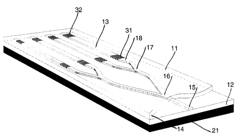
Figure 1 shows a schematic view of an array of 6 buried waveguide lasers, made
in a
combination of doped and un-doped silica and placed on a silicon substrate.
Approximately 12 Nm buffer glass separates the waveguide cores from the
silicon
substrate, and the surface of the top cladding. The individual waveguide
lasers are
spaced by 125 Nm centre-to-centre, and have increasing width. The laser
resonator
structures are defined by Bragg gratings imprinted directly into the waveguide
cores,
using a suitable phasemask (not shown), covering all the waveguides, and
actinic
radiation. The spatial positions of the Bragg gratings in the individual
lasers are illustrated
SUBSTITUTE SHEET (RULE 26)
CA 02385364 2002-03-19
WO 01/22542 PCT/DK00/00521
18
by the alternating closely spaced light and dark areas in the waveguide cores
in opposite
ends. The dimensions are exaggerated for reasons of clarity.
Figure 2A (circle + arrow indicates which axis values should be read ofd shows
a Bragg
wavelength as function of waveguide width, ~,B(w). The curve 42 shows ~,B(w)
for one
polarisation, obtained for waveguides fabricated according to the present
invention. For
consistent fabrication process parameters this curve can be used to design
laser
structures according to Figure 1 having waveguide widths resulting in
equidistantly
spaced output laser wavelengths e.g. placed on the ITU grid. For comparison, a
corresponding curve 41 shows measured laser wavelengths as function of
waveguide
width as obtained from Veasey et al.'. The two curves are shown on the same
scale, with
shifted vertical origins. Note the minute slope of the curve published in
Veasey et al.
Figure 2B shows the effective refractive index as function of waveguide width,
ne"(w), for
the same cases as Figure 2A. Curve 44 is obtained for waveguides fabricated
according
to the present invention and corresponds to curve 42 of Figure 2A. Curve 43 is
obtained
from Veasey et al. and corresponds to curve 41 of Figure 2A.
Figure 3 shows a schematic view of an array of 4 buried planar waveguide
lasers. The
individual lasers are pumped from a single fibre (not shown) butt-coupled to a
single
waveguide which is split using 3 dB power splitters into 4 waveguides coupled
to the array
of 4 waveguide lasers through adiabatic tapers. The Bragg gratings at the far
end are
made highly reflective and spectrally broad compared to the Bragg gratings at
the near
end, thus the laser outputs are predominantly from the near end. The laser
outputs are
multiplexed together by the power splitters into the input waveguide and
collected by the
pump fibre.
Figure 4 shows a measured output spectrum from a four-channel waveguide laser
array
made according to the present invention in a configuration corresponding to
the one
shown in Figure 3. The waveguide laser array structure was designed to 50 GHz
channel
1 D. L. Veasey et al. "Arrays of distributed-Bragg-reflector waveguide lasers
at 1536 nm in
Yb/Er codoped phosphate glass", Appl. Phys. Lett., Vol. 74, No. 6, February
1999, pp.
789 - 791
SUBSTITUTE SHEET (RULE 26)
CA 02385364 2002-03-19
WO 01/22542 PCT/DK00/00521
19
spacing (= 0.41 nm) by selecting four appropriate widths from the design curve
exhibited
on Figure 2A.
Figure 5 shows measured laser output peak positions as function of temperature
corresponding to the spectral trace in Figure 4. As the temperature is
increased the peaks
move towards higher wavelengths with 10.5 pm/°C, however, the spacing
between the
individual channels show no dependence on temperature within the measurement
precision (10 pm) in the temperature interval.
Figure 6 shows a schematic view of an array of 4 buried planar waveguide
lasers coupled
to a 1-to-4 splitter/combiner tree as in Figure 3. This embodiment differs
from the one
depicted in Figure 3 by the employed taper sections inside the waveguide laser
cavities.
Small taper sections are introduced inside each cavity, tapering the cavity
width to a mean
width identical to all the waveguide laser array cavities. This approach helps
equalising
the gain inside the cavities, resulting in a more uniform power output in the
emitted laser
wavelengths. The Bragg wavelengths are not affected by this approach, as the
Bragg
wavelengths are determined by the waveguide width at the grating positions.
The
waveguide widths at the grating positions are not affected by the tapers added
inside the
cavities.
Figure 7 shows the derivative of the design curve exhibited in Figure 2A. To
successfully
fabricate an array of waveguide lasers spanning a large number of standard ITU
channels
using the method according to the present invention, the obtained design curve
must fulfil
two distinct requirements. First, it is mandatory that a wide wavelength range
be
encompassed by the curve. Second, it is crucial that the design curve, ~,B(w),
is a
monotonically increasing function of the waveguide widths w, and that the
derivative is a
softly varying function. A wide wavelength range is needed to encompass a
large number
of standard ITU channels. The softly varying derivative is required, such that
the
incremental waveguide width needed to step from a given ITU channel to the
next ITU
channel neither is too small, nor too large. If very small incremental widths
are required
the spectral position of the laser outputs and hence channel spacing are very
easily
influenced by process fluctuations in the fabrication process.
SUBSTITUTE SHEET (RULE 26)
CA 02385364 2002-03-19
WO 01/22542 PCT/DK00/00521
DETAILED DESCRIPTION
The present invention concerns a multi-wavelength emitting laser device based
on silica-
on-silicon planar optical waveguides. Moreover, it allows for a large span of
the emitted
wavelengths by variation of the dimensions of the employed waveguides, and for
5 subsequent tuning of the emitted wavelengths by forming Bragg gratings in
the
waveguides using actinic radiation. Said Bragg gratings can be individually
tuned using a
focused beam of actinic radiation. It also provides a multi-wavelength
emitting laser
device with superior thermal and mechanical stability towards external
influences.
10 With reference to Figure 1, these features are achieved by burying, in a
planar silica
structure 12 + 14 on a silicon substrate 21, closely spaced parallel nearly
rectangular
silica waveguides with predetermined variation in widths translating into a
predetermined
variation in effective refractive indices. The waveguide cores 13 are co-doped
at least with
germanium and erbium, and preferably also aluminium and ytterbium.
Furthermore, Bragg
15 gratings 31 and 32 are imprinted into the waveguides by irradiating the
waveguides with
coherent actinic radiation through a phasemask. Those Bragg gratings
constitute a laser
resonator structure in each of the waveguides, emitting in different
predetermined
wavelengths.
20 The basic structure of the waveguide is traditional and consists of
substrate 21 -
undercladding 12 - waveguide cores - topcladding 14 reflowed over the cores.
Some
general features of the waveguide structure, its properties and the Bragg
gratings will now
be given, and a more detailed description of the fabrication process will be
given later on.
The waveguide cores are placed on a silica buffer layer 12 of sufficient
thickness, to
render coupling of optical energy from the waveguides to the substrate 21
negligible. For
typical waveguides having a refractive index step of approximately 10-z
compared to the
silica buffer layer 12, a thickness of 10 Nm or more is preferred for the
buffer layer. The
silica buffer layer 12 is obtained by thermally oxidising the silicon
substrate, or
alternatively, by depositing using a suitable silica deposition method a layer
of silica on at
least one side of the silicon substrate.
Silicon has thermal conductivity two orders of magnitude larger than silica,
and can
therefore eliminate local temperature fluctuations from external influences,
ensuring
SUBSTITUTE SHEET (RULE 26)
CA 02385364 2002-03-19
WO 01/22542 PCT/DK00/00521
21
consistent laser channel spacing. Furthermore, mechanical stability is
obtained by the
high out-of-plane bending stiffness property of the silicon substrate 21.
Preferably, the waveguide cores 13 are co-doped at least with germanium and
erbium,
and in most cases also with aluminium and ytterbium, in order to create
amplifying
waveguides when the device is pumped around 980 nm or 1480 nm. For typical
waveguide cores having a refractive index step of approximately 10-2 compared
to
thermally oxidised silicon the preferred height of the waveguide cores is
approximately
3pm or more.
In order to establish the waveguides, the cores are covered with a top
cladding layer 14 of
reflowable boron and phosphorous doped silica glass having a refractive index
close to
that of the silica buffer 12. Alternatively, the waveguide cores are first
covered first with a
thin layer of undoped silica glass and subsequently with a layer of reflowable
boron and
phosphorous doped silica glass. Both glasses having a refractive index close
to that of the
silica buffer. It is preferred that the thickness of the first undoped layer
of silica glass is
less than approximately 2 Nm. As another alternative, a top cladding 14
entirely made
from undoped silica is used, having a refractive index close to that of the
silica buffer 12.
The total thickness of the top cladding as measured from the top of a
waveguide core to
the surface of the top cladding is at least approximately 10 Nm.
The waveguides should be closely spaced, although not so close that
significant
exchange of optical energy takes place between neighbouring waveguides. For
typical
waveguides having a refractive index step of approximately 10'2 compared to
the silica
buffer layer, a waveguide separation of more than approximately 50 Nm is
preferred. For
easy coupling of a multitude of waveguide lasers to a multitude of fibres a
separation of
the waveguides corresponding to the fibre separation in a fibre ribbon is
preferred.
As mentioned earlier, Bragg gratings are imprinted into the waveguides by
irradiating the
waveguides with coherent actinic radiation through a phasemask. This is to
establish laser
cavities in the amplifying waveguide cores. The reflected wavelengths are
determined by
the effective refractive index pertaining to a mode in the waveguide, and by
the
phasemask period, according to the equation:
~.a - neff(w) X n (1 ).
SUBSTITUTE SHEET (RULE 26)
CA 02385364 2002-03-19
WO 01/22542 PCT/DK00/00521
22
~,B is the reflected wavelength (and hence the laser wavelength), ne"(w) the
effective
refractive index of a waveguide of width w, and A is the phasemask period.
The width w of a waveguide is defined as the width of the etched core profile
before
deposition and annealing of the topcladding, hence the width as determined by
the
phasemask in the UV writing procedure. More precisely, w is the width of the
waveguide
core measured in a direction substantially parallel to the substrate and
normal to the
waveguide centre axis, in a height corresponding to half the height of the
core layer. In
most cases in this text, the width will refer to the width at the position of
the DBR gratings,
31 and 32 in Figure 1.
The effective refractive index, neff, is the refractive index experienced by
light propagating
in some transverse mode through the waveguide. The electromagnetic (EM) field
strength
of a transverse mode will typically reach into the surrounding cladding.
Thereby, the
effective refractive index experienced will be a combination of the refractive
index n~~e of
the core and n~,add~"9 of the cladding region. If the core is narrow, a large
part of the EM
field strength of a transverse mode will reach into the cladding region and
hence neff will
be highly influenced by n~~adding~ Adjusting the width w of the core thereby
means adjusting
the contributions from n~~e and n~~adding~ and thereby neff(w).
Two lasers being equal except from a difference Ow in the waveguide width w
(and hence
a difference one" in the effective refractive index neff(w)) at the position
of the grating, will
have a difference ~~,8 in their laser wavelength ~,8. This property, a change
ow leads to a
change One" and thereby ~~,8, is an inherent property of the waveguide
materials and
geometry. The dependency of ~,B and neff on the width of the waveguide is
illustrated in
Figure 2A and B respectively (unless otherwise stated, reference to Figure 2A
and B will
be to the curves 42 and 44, where circle + arrow indicates that values should
be read off
the left axis) which shows ~,B(w) and neff(w) as function of waveguide width,
~,B(w), curve
for one polarisation, obtained for waveguides fabricated according to the
present
invention. Since the waveguides used in curves 42 and 44 in Figure 2A and B
all have the
same grating pitch A, the dependency neff(w) is analogous to ~,B(w) (formula
1) and, for
use in defining the waveguide properties, a more fundamental entity. The
background of
Figure 2A and B will be described in greater detail later on.
SUBSTITUTE SHEET (RULE 26)
CA 02385364 2002-03-19
WO 01/22542 PCT/DK00/00521
23
In order to characterise the ability to tune wavelength by adjusting the width
of a
waveguide, we define dne~/dw, the derivative of ne~,(w), as the important
parameter
expressing the change in laser wavelength for a given change in the width, of
the
waveguide laser, at the position of the Bragg gratings. It is preferable that
dneff/dw is of
considerable size in order to be able to span a broad wavelength band by
varying only the
width. On the other hand, a too large value of dneff/dw, which is proportional
to the slope
of the curve in Figure 2B, may be disadvantageous because of a
hypersensitivity of the
reflected wavelength upon the width.
As seen from Figure 2B, the slope of the curve becomes small as the width
increases to
above 12um. This is because, as the width of the waveguide core and of the
relevant
transverse mode becomes comparable in size, the contribution from n~,add~~9
becomes
insignificant, and ne" ~ n~~e for all practical purposes. A similar effect
will arise in the other
end of the curve, when the width of the core becomes small, and the
contribution from
n~~e becomes insignificant.
The present invention concerns planar waveguide lasers, where at least one of
the
reflecting means constituting the laser resonator is a Bragg grating, which
are
characterised by their value of dne~Jdw, such as to optimise wavelength tuning
by varying
the width w. Figure 7 shows a plot 71 of d~.B/dw = A x dne~/dw as a function
of w. It is
seen that d~,~/dw is larger than 0.2 nm/~m for the given widths. Since in the
given case
the grating pitch was A = 1071 nm, the corresponding minimum value of dne~/dw
is 1.9 x
10~ pm-'. The highest value of d~,~/dw found in the prior art, Veasey et al.,
is ~ 0.1 nm/pm
corresponding to dne~/dw = 1.0 x 10~ ~m~' (A = 1015.6 nm). The reason for
these
differences belongs to the difference in refractive index profile of the
waveguide core,
which will be described in further detail later.
Preferably dneff/dw is in the interval between 1.0 x 10~ p.m-' and 20.0 x 10~'
pm-' in order to
ensure a reasonable wavelength span for varying widths and on the other hand a
reasonable sensitivity of the tuning.
By exploiting and optimising the above relations, it is obtained that
variation of waveguide
widths w of the well-defined nearly rectangular waveguides give rise to a
large variation in
the effective refractive index neff(w), and hence laser wavelength ~.8, making
it possible to
span several standard ITU channels. In other word, waveguide lasers with Bragg
gratings
SUBSTITUTE SHEET (RULE 26)
CA 02385364 2002-03-19
WO 01/22542 PCT/DK00/00521
24
having the same spatial periodicity can be tuned by varying their width, which
is a very
convenient and easy way of tuning the laser wavelength.
It is possible to employ a phasemask that contains several (N) parallel
gratings of varying,
definite period, A,, AZ, ... AN, co-ordinated with several groups of closely
spaced
waveguides on the wafer, each group consisting of waveguides having varying
widths.
Due to the close spacing, it is possible to align the phasemask to the
underlying
waveguides to form a multitude of groups containing a multitude of lasers all
with distinct
predetermined wavelengths. Such an arrangement can span an even wider range of
standard ITU channels, since tuning properties of the grating pitch and the
waveguide
width are combined.
The laser frequency of individual lasers may be separated by any interval
larger than the
linewidth of a single mode, so as to agree with the spacing of ITU channels.
Typical ITU
standards are 100 GHz and 50 GHz for each channel, corresponding to wavelength
intervals of 0.82 nm and 0.41 nm respectively. However, it is feasible with
the multi-
wavelength emitting laser device of the present invention to have centre
frequencies of
single modes separated by 25 GHz, 12.5 GHz or 10.0 GHz or any frequency
interval in
between the mentioned intervals. Since an ITU channel allows for small (12.5%)
variations these frequency separations translates into intervals 75 - 125 GHz,
37.5 - 62.5
GHz, 18.75 - 31.25 GHz, 9.375 - 15.615 GHz and 7.5 - 12.5 GHz
By placing the waveguides in close proximity, macroscopic variations in the
silica layers
across the substrate can be neglected. Thereby, the variation of the waveguide
widths
translates directly into a variation of the effective refractive index of the
waveguides. Also,
it is obtained in that macroscopic variations in the photolithography and
etching steps,
utilised in the definition of the waveguide cores, can be neglected. Further,
it is obtained in
that a large number of waveguides can fit under a standard phasemask at one
time, and
that Bragg gratings can be imprinted with a single exposure session using
coherent
actinic radiation. Thus, Bragg gratings can be made simultaneously, with a
high degree of
precision, in several well-defined waveguides, making it possible to precisely
control the
position of the emitted wavelengths.
SUBSTITUTE SHEET (RULE 26)
CA 02385364 2002-03-19
WO 01/22542 PCT/DK00/00521
Using UV-writing, it is furthermore obtained that the precise position of the
emitted
wavelengths can be fine-tuned in a post processing step, using a focused beam
of actinic
radiation, scanning the previously fabricated Bragg gratings.
5 The multi-wavelength emitting laser resonator structures can be realised in
several ways,
with the laser resonator structures are made either as distributed Bragg-
reflector or
distributed feedback types. Some of these will be discussed, with reference to
Figure 1, 3
and 6. In most cases, the Bragg gratings 31 and 32 are formed by exposure with
coherent
actinic radiation through a suitable phasemask. In some cases one of the
gratings can be
10 replaced by a highly reflective dielectric mirror. Typically, the waveguide
structure is high
pressure loaded with deuterium or hydrogen previous to the exposure.
In a first embodiment, the laser resonator structures is of the distributed
Bragg-reflector
type, where one Bragg grating 32 is substituted by another highly reflective
means, such
15 as a dielectric mirror (not shown), positioned at the facets on one end of
the waveguides.
The other Bragg grating 31 is then formed by exposure of the waveguides with
coherent
actinic radiation through a suitable phasemask.
In a second embodiment, the multi-wavelength emitting laser resonator
structure is of the
20 distributed Bragg-reflector type, where the Bragg-reflector 32 in one end
has very high
reflectance and is very broad band. The Bragg-reflector 31 at the other end
then exhibit
lower reflectance and only reflects in a very narrow wavelength range around
each of the
predetermined wavelengths.
25 Having formed the multi-wavelength emitting waveguide laser resonator
structure, it is
often desirable to multiplex the laser outputs together. This is shown in
Figure 3, where
the multiplexing is carried out by power splitters 16 and 17 into the input
waveguide 15.
The waveguide are coupled to the multiplexers through adiabatic tapers 18.
In a third preferred embodiment, the multi-wavelength emitting waveguide laser
resonator
structure is formed using two sampled Bragg gratings, having constant but
slightly
different spacing between reflection peaks in their respective spectra. A
sampled grating
consists of a number of short grating sections with equal length L1 separated
an equal
distance L2 from each other. Sampled gratings offer multi-peak reflection with
good
control over the spectral distance between the peaks. By slightly varying the
effective
SUBSTITUTE SHEET (RULE 26)
CA 02385364 2002-03-19
WO 01/22542 PCT/DK00/00521
26
refractive index at the position of one of the sampled gratings, the
reflection peak
spectrum wilt move slightly. As the reflection peak spectrum moves, different
peaks in the
two reflection spectra will overlap at different times, selecting different
laser wavelengths.
In this way a large number of ITU channels can be obtained by slight variation
of the
effective refractive index through the waveguide width at the position of one
of the
sampled gratings.
In a fourth embodiment, shown in Figure 6, the multi-wavelength emitting
waveguide laser
resonator structure is formed using any of the above reflector configurations.
In order for
the laser cavities to be of the same size, tapered parts 19 are defined close
to the gratings
31 and 32. This permits equal volumes of amplifying waveguide core 13 in the
cavities at
the same time as a variation in the waveguide width w at the position of the
gratings for
tuning purposes. This tapering can be favourable because the output power to
some
degree depends on the size of the active regions, and it is desired to have
equal output
powers from the lasers.
The optical waveguide structure 11 holding an array of planar waveguide lasers
is
prepared by a combination of different standard clean room thin film
techniques, such as
thermal oxidation of silicon, Plasma Enhanced Chemical Vapour Deposition
(PECVD) of
doped and un-doped silica, photolithography and Reactive Ion Etching (RIE) of
silica.
First, a standard silicon wafer 21 is RCA-cleaned and thermally oxidised to
give an oxide
layer 12 with a thickness of at least 10 Nm. The resulting oxide is to be used
as buffer
cladding for the waveguide cores. Second, using PECVD an approximately 5 Nm
thick
layer of aluminium- and erbium-doped germanosilicate core glass is deposited
on the top
of the silica buffer layer, and subsequently annealed. The PECVD process uses
silane,
germane and nitrous oxide as precursors for the deposition of the
germanosilicate.
Aluminium and erbium are supplied from a liquid source containing AI- and Er-
chelate
dissolved in an organic solution. The liquid flow is metered, flash-evaporated
and
subsequently driven into the PECVD reactor with a carrier gas.
Waveguide cores 13 are defined in the core glass layer using standard
photolithography
and RIE. Finally, the etched cores are covered with an approximately 12 Nm
thick
cladding layer 14 of boron- and phosphorous doped silica, which is
subsequently
annealed. By employing a top cladding structure composed of a first thin layer
of undoped
SUBSTITUTE SHEET (RULE 26)
CA 02385364 2002-03-19
WO 01/22542 PCT/DK00/00521
27
silica glass followed by a layer of boron- and phosphorous-doped glass, inter-
diffusion of
dopants between the doped top cladding layer and the core is minimised, hence
maintaining the advantageous nearly rectangular refractive index profile. The
melting
point for the doped core material is so high that the final annealing of the
topcladding does
not alter the nearly rectangular index profile of the core significantly.
Note, that the glass layers 12 and 14, and waveguide cores 13 described above
may be
formed by other means, and may contain further dopants. For example, the
silica layers
can be deposited using flame hydrolysis deposition, and may be doped using
e.g. solution
doping. Also the dopant ytterbium may conveniently be added to the core glass
structure.
The Bragg gratings 31 and 32, used to define the laser cavities are imprinted
into the
waveguide cores using 248 nm excimer UV-laser light through a zero-order
pulled
phasemask with a fixed periodicity of 1071 nm. Any type of actinic light can
in principle be
applied for writing. The used 3 mm wide and 50 mm long phasemask covers the
waveguide array during exposure. By scanning the UV beam, exposure is
performed in
both ends of the waveguide cores 13 constituting the waveguide array 11,
leaving a
region unexposed in the centre.
Prior to the exposure session, the wafer with the completed waveguide
structure 11 is
high-pressure deuterium loaded to significantly enhance photosensitivity of
the core glass.
After the Bragg gratings 31 and 32 have been fabricated in the exposure
session, the
waveguide laser array is post annealed at approximately 200 degrees centigrade
for
typically half an hour to stabilise the gratings by removing short-lived
unstable
components of the UV-induced refractive index change.
A single waveguide laser fabricated according to the above described method,
have given
output of 0.4 mW at 1553 nm for a pumping power of 265 mW at 979 nm.
In order to obtain a precisely defined constant channel spacing between the
laser outputs
it is necessary to know the Bragg wavelength as function of the waveguide
width, ~,B(w).
This function, of which an example is displayed in Figure 2A, has a number of
constant
parameters such as the waveguide height and the refractive index step, as well
as more
subtle parameters from the fabrication process, such as the exact waveguide
core shape
and e.g. annealing influences.
SUBSTITUTE SHEET (RULE 26)
CA 02385364 2002-03-19
WO 01/22542 PCT/DK00/00521
28
Although, in principle, it is possible to calculate ~,B(w) by calculating
neff(w), it is preferred
that ~,B(w) is determined experimentally. This is done by imprinting weak
Bragg gratings
into an array of waveguide cores of increasing width w, and then for each
waveguide
measure the Bragg wavelength. The resulting ~,B(w) 42 as shown in Figure 2A is
then
used as a design function pertaining to the applied waveguide fabrication
process and the
used phasemask. However, it is straightforward to obtain a new ~.e(w) using
the same
waveguide fabrication process by using a phasemask with a different period A.
From ~,B(w) the waveguide widths resulting in a constant channel spacing are
inferred. A
new photomask can then be designed holding a pattern defining waveguides of
correct
width resulting in the desired laser structures. Therefore, a curve ~,B(w) is
called a design
curve.
The invention is further illustrated by the following examples of preparation
of a design
curve ~.e(w), and another example where said design curve ~.B(w) is used to
fabricate a
four-channel laser device having a multiplexed nearly equidistantly channel
spacing of 50
GHz. Also an example of temperature tuning and temperature stability of the
laser output
will be shown.
Example 1
A design curve 42 as given in Figure 2A showing the Bragg wavelength ~,B(w) as
function
of waveguide width, or alternatively Figure 2B showing neff(w), is needed for
the
fabrication of waveguide laser structures emitting at predetermined
wavelengths.
For this purpose a buried waveguide structure was made holding an array of 30
waveguide lasers designed conceptually as depicted in Figure 1. The individual
cavities
(formed in the waveguide cores 13) of the array were spaced 125 Nm centre-to-
centre,
and had nominal widths from 4 Nm to 12.7 Nm in constant step of 0.3 Nm. A
single set of
Bragg gratings 31 were imprinted into the waveguide cores 13, thus the Bragg
gratings 32
were omitted. The Bragg gratings 31 were made using UV-exposure (248 nm)
through a
zero-order pulled phasemask with a fixed periodicity of 1071 nm. Spectrally
broad light
from an erbium-doped fibre based amplified spontaneous emission (ASE) light
source
was successively coupled to each of the waveguide cores 13 using a butt-
coupled fibre.
SUBSTITUTE SHEET (RULE 26)
CA 02385364 2002-03-19
WO 01/22542 PCT/DK00/00521
29
Light transmitted through the waveguide core 13 and the grating 31 was
collected at the
opposite end using another butt-coupled fibre, and subsequently fed to a
spectrum
analyser where the position of the transmission dip was recorded, ultimately
yielding the
curve 42 on Figure 2A. The curve 42 shows the versatility of the fabrication
method
according to the present invention. By varying the widths of the waveguide
cores 13 from
4 Nm to 12.7 Nm a Bragg wavelength span of more than 5 nm is obtained, making
it
possible to span several standard ITU channels.
Example 2
For the purpose of demonstrating the applicability of the method according to
the present
invention, a four-channel planar waveguide laser array with integrated power
splitters/combiners was designed, using the design curve from example 1, and
fabricated.
In a silicon substrate 21 an approximately 12 Nm thick buffer layer 12 of
thermal oxide
was grown, as shown in Figure 3. An approximately 5 Nm thick layer of erbium
and
aluminium doped germanosilicate core glass was deposited using PECVD and
subsequently annealed. Waveguide widths that should render it possible to
fabricate an
array of lasers with 50 GHz channel spacing were inferred from the curve 42 on
Figure
2A. The 4 waveguides 13 in the laser array design were coupled through
adiabatic tapers
18 to a 1-to-4 y-splitter/combiner tree 16 and 17, ending in one waveguide 15.
The
waveguide laser array and splitter/combiner structure was transferred into the
erbium and
aluminium germanosilicate using a combination of standard clean room
photolithography
and RIE. Finally, the etched structure was covered by a layer 14 of top
cladding glass,
and annealed.
Prior to Bragg grating fabrication, the entire structure was deuterium loaded
to
significantly increase the photosensitivity of the core glass. Bragg gratings
with lengths
and strengths of approximately 10 mm (reflection > 99.9 %, 1 nm wide) 31, and
10 mm
(reflection approximately 95 %, 3 dB width of < 0.3 nm) 32 were imprinted into
the
waveguides 13, as described in example 1, leaving a 10 mm region in between
unexposed. The comparatively high reflectance of the Bragg gratings 32 was
made so
that laser power was primarily emitted from the individual laser through the
gratings 31,
and into the 1-to-4 splitter/combiner structure and fnally to the waveguide 15
back into the
launching fibre. The collected resulting laser output was then separated from
the pump
using a fibre WDM and analysed by an optical spectrum analyser.
SUBSTITUTE SHEET (RULE 26)
CA 02385364 2002-03-19
WO 01/22542 PCT/DK00/00521
The spectral output, when the laser array is pumped at 980 nm, is shown in
Figure 4,
where the peaks 51, 52, 53, and 54 each represents an output from 1 of 4 of
the lasers in
the planar waveguide laser array. The widths of the waveguides 13 were
designed to give
an equidistant channel spacing of 50 GHz. Examining the position of the 4
peaks 51 - 54
5 yields that the channel spacing is almost constant, with a channel spacing
of 51.1 GHz
between peaks 51 and 52, 45.3 GHz between peaks 52 and 53, and finally 41.4
GHz
between peaks 53 and 54.
Example 3
For the purpose of demonstrating the excellent temperature stability and
temperature
10 tuning possibilities of a planar waveguide laser array fabricated according
to the present
invention, the 4-channel laser array described in example 2 was put to test.
The waveguide laser array was placed on a temperature controllable mount, and
a
pump/collecting fibre was butt-coupled to the single waveguide 15, and through
a fibre
WDM leading the collected laser outputs to an optical spectrum analyser. The
15 temperature of the mount was linearly vamped from 13.5 to 76 degrees
centigrade, and
temperature as well as corresponding peak positions for each of the 4 laser
outputs was
recorded. The results of this measurement are shown in Figure 5, where the
laser
wavelength position of each of the 4 laser outputs from the array is plotted
as function of
mount temperature.
The curves on Figure 5 show excellent channel spacing stability as the
temperature is
raised. The spacing between the individual channels show no dependence on
temperature within the measurement precision (10 pm) in the temperature
interval from
13.5 to 76 degrees centigrade. As the temperature of the mount is raised, the
output
peaks from the laser array move linearly towards higher laser wavelengths with
a rate of
10.5 pm/degree centigrade. As the channel spacing between each of the laser
outputs
remain constant, this collective translation of the outputs can be used to
precisely position
the outputs from the laser array on a number of consecutive ITU channels.
In the table below are listed ITU wavelengths for the ITU channels
(frequencies) 193.00
THz to 193.20 THz, as well as laser wavelengths at two different temperatures
for the
device discussed in the present example.
ITU - Laser output
wavelengths
(nm)
THz Wavelength (nm) @ 16 "C @ 57.7 "C
SUBSTITUTE SHEET (RULE 26)
CA 02385364 2002-03-19
WO 01/22542 PCT/DK00/00521
31
193.00 1553.329 1553.292
193.05 1552.926 1552.866 1552.948
193.10 1552.524 1552.520 1552.578
193.15 1552.122 1552.152 1552.158
193.20 1551.721 1551.736
The presented numbers in the table clearly show that it is possible to
position the outputs
from the planar waveguide laser array on the ITU grid and, furthermore, to
select between
different sets of channels, depending upon the temperature.
SUBSTITUTE SHEET (RULE 26)