Note: Descriptions are shown in the official language in which they were submitted.
CA 02385429 2002-05-08
1
METHOD AND SYSTEM FOR TRANSMITTING INFORMATION
IN AN OPTICAL COMMUNICATION SYSTEM USING
DISTRIBUTED AMPLIFICATION
TECHNICAL FIELD OF THE INVENTION
The present invention relates generally to optical
communication systems, and more particularly to a method
and system for transmitting information in an optical
communication system using distributed amplification.
BACKGROUND OF THE INVENTION
Telecommunications systems, cable television systems
and data communication networks use optical networks to
rapidly convey large amounts of information between
remote points. In an optical network, information is
conveyed in the form of optical signals through optical
fibers. Optical fibers are thin strands of glass capable
of transmitting the signals over long distances with very
low loss.
Optical networks often employ wavelength division
multiplexing (WDM) to increase transmission capacity. In
a WDM network, a number of optical channels are carried
in each fiber at disparate wavelengths. Network capacity
is increased as a multiple of the number of wavelengths,
or channels, in each fiber.
The maximum distance that a signal can be
transmitted in a WDM or other optical network without
amplification is limited by absorption, scattering and
other loss associated with the optical fiber. To
transmit signals over long distances, optical networks
typically include a number of discrete amplifiers spaced
along each fiber route. The discrete amplifiers boost
CA 02385429 2011-03-21
2
received signals to compensate for transmission losses in
the fiber.
Signals may also be boosted in the fiber using Raman
effect amplification. In the Raman effect, optical
signals traveling in the fiber are amplified by the
presence of a lower wavelength pump light traveling in
the same fiber. The pump light may travel forward with
the signal or backwards in reverse of the signal.
Because forward pumping amplification causes cross talk
between channels in WDM systems due to cross gain
modulation (XGM), reverse pumping amplification is
typically used in connection with WDM and other
multichannel systems. This limits the use of Raman
effect amplification in multichannel systems to
unidirectional transmission fibers and prevents bi-
directional distributed amplification.
SUMMARY OF THE INVENTION
The present invention provides an improved method
and system for transmitting information in an optical
communication system using distributed amplification. In
a particular embodiment, phase, frequency or other non-
intensity modulated information signals are used to
transmit data across an optical link which allows for
forward, or co-pumping, and backward, or counter-pumping,
distributed Raman amplification (DRA) while still
providing a superior signal-to-noise ratio.
CA 02385429 2011-03-21
2a
Certain exemplary embodiments can provide a method for
transmitting information in an optical communication system,
comprising: generating a plurality of optical information
signals each comprising a wavelength distinct carrier signal
having the non-intensity characteristic modulated with a data
signal; multiplexing the plurality of optical information
signals to generate a wavelength division multiplexed (WDM)
signal, the WDM signal having a minimum channel spacing that
is greater than (N+0.4)B and less than (N+0.6)B, where B
comprises the symbol rate of the WDM signal and N is an
integer; transmitting the WDM signal over an optical link;
and amplifying the WDM signal over a length of the optical
link with a plurality of co-launched amplification signals
traveling in a same direction as the WDM signal in the
optical link.
Certain exemplary embodiments can provide an optical
communication system, comprising: an optical sender operable
to generate a plurality of optical information signals each
comprising a wavelength distinct carrier signal having the
non-intensity characteristic modulated with a data signal,
multiplex the plurality of optical information signals to
generate a wavelength division multiplexed (WDM) signal and
transmit the WDM signal over the optical link, the WDM signal
having a minimum channel spacing that is greater than
(N+0.4)B and less than (N+0.6)B, where B comprises the symbol
rate of the WDM signal and N is an integer; an optical link
operable to transmit the WDM signal; and a distributed
amplifier comprising a pump laser operable to co-launch an
amplification signal traveling in a same direction as the WDM
signal, the co-launch amplification signal operable to
amplify the WDM signal over a length of the optical link.
CA 02385429 2011-03-21
2b
Other embodiments provide a method and system for
transmitting information in an optical communication system
including modulating an non-intensity characteristic of an
optical carrier signal with a data signal to generate an
optical information signal. The optical information signal is
CA 02385429 2002-05-08
3
transmitted over an optical link. The optical
information signal is amplified over a length of the
optical link with a co-launched amplification signal
traveling in the optical link in a same direction as the
optical information signal.
More specifically, in accordance with a particular
embodiment of the present invention, the optical
information signal is amplified with the co-launched
amplification signal by DRA. In this and other
embodiments, the optical information signal may be
multiplexed with other optical information signals to
generate a wavelength division multiplexed (WDM) signal
for transmission over the optical link. The non-
intensity modulation characteristic may comprise the
phase and/or frequency of the carrier signal.
In accordance with another aspect of the present
invention, the optical information signal may be
remodulated with a transmission clock frequency using an
intensity modulator to generate a multimodulated signal.
The multimodulated signal is transmitted over the optical
link and amplified over the length of the optical link
with the co-launched amplification signal.
Technical advantages of the present invention
include providing an improved method and system for
transmitting information in an optical communication
system using distributed amplification. In a particular
embodiment, phase or frequency modulation is used to
transmit data over an optical fiber to allow bi-
directional DRA without cross talk between channels due
to cross-gain modulation (XGM). As a result, signals may
be transmitted over longer distances with high signal-to-
noise ratios and DRA may be used in connection with long-
haul optical transmission systems.
CA 02385429 2002-05-08
4
Another technical advantage of one or more
embodiments of the present: invention includes providing a
bi-directional multichannel optical communication system
using distributed amplification. In particular, data is
transported using non-intensity modulation to allow data
transmission in the forward and reverse directions of DRA
pump lasers. Accordingly, amplification of bi-
directional communication systems are improved and
distances over which data may be communicated bi-
directionally is increased.
Still another technical advantage of one or more
embodiments of the present invention include providing an
optical transmission system with improved power
tolerance. In particular, data is modulated using phase
or frequency shift keying to eliminate XGM with the
resulting signal being remodulated with the transmission
clock using intensity modulation. As a result, non-
linear and chromatic effects creating signal recovery
problems at phase edges are minimized while still
allowing for forward. and/or reverse DRA and high signal-
to-noise ratios.
Other technical advantages of the present invention
will be readily apparent to one skilled in the art from
the following figures, description and claims.
BRIEF DESCRIPTION OF THE DRAWINGS
For a more complete understanding of the present
invention and its advantages, reference is now made to
the following description taken in conjunction with the
accompanying drawings, wherein like numerals represent
like parts, in which:
CA 02385429 2002-05-08
FIGURE 1 is a block diagram illustrating an optical
communication system using distributed amplification in
accordance with one embodiment of the present invention;
FIGURE 2 is a block diagram illustrating the optical
5 sender of FIGURE 1 in accordance with one embodiment of
the present invention;
FIGURES 3A-C are diagrams illustrating non-intensity
modulated signals for transmission in the optical
communication system of FIGURE 1 in accordance with
several embodiments of the present invention;
FIGURE 4 is a block diagram illustrating the optical
sender of FIGURE 1 in accordance with another embodiment
of the present invention;
FIGURE 5 is a diagram illustrating the optical
waveform generated by the optical sender of FIGURE 4 in
accordance with one embodiment of the present invention;
FIGURE 6 is a block diagram illustrating the optical
receiver of FIGURE 1 in accordance with one embodiment of
the present invention;
FIGURE 7-is a diagram illustrating the frequency
response of the asymmetric Mach-Zender interferometer of
FIGURE 6 in accordance with one embodiment of the present
invention;
FIGURES 8A-C are block diagrams illustrating the
demultiplexer of FIGURE 1 in accordance with several
embodiments of the present invention;
FIGURE 9 is a flow diagram illustrating a method for
communicating data over an optical communication system
using distributed amplification in accordance with one
embodiment of the present invention;
FIGURE 10 is a block diagram illustrating a bi-
directional optical communication system using
CA 02385429 2002-05-08
6
distributed amplification in accordance with one
embodiment of the present invention;
FIGURE 11 is a block diagram illustrating the
optical sender and receiver of FIGURE 1 in accordance
with another embodiment of the present invention;
FIGURE 12 is a block diagram illustrating the
modulator of FIGURE 11 in accordance with one embodiment
of the present invention;
FIGURE 13 is a flow diagram illustrating a method
for tuning the modulation depth of an optical signal
based on receiver side information in accordance with one
embodiment of the present invention;
FIGURE 14 is a block diagram illustrating an optical
communication system distributing a clock signal in an
information channel in accordance with one embodiment of
the present invention; and
FIGURE 15 is a block diagram illustrating an optical
receiver for extracting a clock signal from a
multimodulated signal in accordance with one embodiment
of the present invention.
DETAILED DESCRIPTION OF THE INVENTION
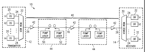
FIGURE 1 illustrates an optical communication system
10 in accordance with one embodiment of the present
invention. In this embodiment, the optical communication
system 10 is a wavelength division multiplexed (WDM)
system in which a number of optical channels are carried
over a common path at disparate wavelengths. It will be
understood that the optical communication system 10 may
comprise other suitable single channel, multichannel or
bi-directional transmission systems.
Referring to FIGURE 1, the WDM system 10 includes a
WDM transmitter 12 at a source end point and a WDM
CA 02385429 2002-05-08
7
receiver 14 at a destination end point coupled together
by an optical link 16. The WDM transmitter 12 transmits
data in a plurality of optical signals, or channels, over
the optical link 16 to the remotely located WDM receiver
14. Spacing between the channels is selected to avoid or
minimize cross talk between adjacent channels. In one
embodiment, as described in more detail below, minimum
channel spacing (df) comprises a multiple of the
transmission symbol and/or bit rate (B) within 0.4 to 0.6
of an integer (N). Expressed mathematically:
(N+0.4)B<df<(N+0.6)B. This suppresses neighboring
channel cross talk. It will be understood that channel
spacing may be suitably varied without departing from the
scope of the present invention.
The WDM transmitter 12 includes a plurality of
optical senders 20 and a WDM multiplexer 22. Each
optical sender 20 generates an optical information signal
24 on one of a set of distinct wavelengths X 1, k 2 ... kn
at the channel spacing. The optical information signals
24 comprise optical signals with at least one
characteristic modulated to encode audio, video, textual,
real-time, non-real--time or other suitable data. The
optical information signals 24 are multiplexed into a
single WDM signal 26 by the WDM multiplexer 22 for
transmission on the optical link 16. It will be
understood that the optical information signals 24 may be
otherwise suitably combined into the WDM signal 26. The
WDM signal is transmitted in the synchronous optical
network (SONET) or other suitable format.
The WDM receiver 14 receives, separates and decodes
the optical information signals 24 to recover the
included data. In one embodiment, the WDM receiver 14
includes a WDM dernultiplexer 30 and a plurality of
CA 02385429 2002-05-08
8
optical receivers 32. The WDM demultiplexer 30
demultiplexes the optical information signals 24 from the
single WDM signal 26 and sends each optical information
signal 24 to a corresponding optical receiver 32. Each
optical receiver 32 optically or electrically recovers
the encoded data from the corresponding signal 24. As
used herein, the term each means every one of at least a
subset of the identified items.
The optical link 16 comprises optical fiber or other
suitable medium in which optical signals may be
transmitted with low loss. Interposed along the optical
link 16 are one or more optical amplifiers 40. The
optical amplifiers 40 increase the strength, or boost,
one or more of the optical information signals 24, and
thus the WDM signal 26, without the need for optical-to-
electrical conversion.
In one embodiment, the optical amplifiers 40
comprise discrete amplifiers 42 and distributed
amplifiers 44. The discrete amplifiers 42 comprise rare
earth doped fiber amplifiers, such as erbium doped fiber
amplifiers (EDFAs), and other suitable amplifiers
operable to amplify the WDM signal 26 at a point in the
optical link 16.
The distributed amplifiers 44 amplify the WDM signal
26 along an extended length of the optical link 16. In
one embodiment, the distributed amplifiers 44 comprise
bi-directional distributed Raman amplifiers (DRA). Each
bi-directional DRA 44 includes a forward, or co-pumping
source laser 50 coupled to the optical link 16 at a
beginning of the amplifier 44 and a backward, or counter-
pumping source laser 52 coupled to the optical link 16 at
an end of the amplifier 44. It will be understood that
the co-pumping and counter-pumping source lasers 50 and
CA 02385429 2002-05-08
9
52 may amplify disparate or only partially overlapping
lengths of the optical link 16.
The Raman pump sources 50 and 52 comprise
semiconductor or other suitable lasers capable of
generating a pump light, or amplification signal, capable
of amplifying the WDM signal 26 including one, more or
all of the included optical information signals 24. The
pump sources 50 and. 52 may be depolarized, polarization
scrambled or polarization multiplexed to minimize
polarization sensitivity of Raman gain.
The amplification signal from the co-pumping laser
52 is launched in the direction of travel of the WDM
signal 26 and thus co-propagated with the WDM signal 26
at substantially the same speed and/or a slight or other
suitable velocity mismatch. The amplification signal
from the counter-pumping laser 52 is launched in a
direction of travel opposite that of the WDM signal 26
and thus is counter-propagated with respect to the WDM
signal 26. The amplification signals may travel in
opposite directions simultaneously at the same or other
suitable speed.
The amplification signals comprise one or more high
power lights or waves at a lower wavelength than the
signal or signals to be amplified. As the amplification
signal travels in the optical link 16, it scatters off
atoms in the link 16, loses some energy to the atoms and
continues with the same wavelength as the amplified
signal or signals. In this way, the amplified signal
acquires energy over many miles or kilometers in that it
is represented by more photons. For the WDM signal 26,
the co-pumping and counter-pumping lasers 50 and 52 may
each comprise several different pump wavelengths that are
CA 02385429 2002-05-08
used together to amplify each of the wavelength distincts
optical information signals 24.
In one embodiment, as described in more detail
below, a non-intensity characteristic of a carrier signal
5 is modulated with the data signal at each optical sender
20. The non-intensity characteristic comprises phase,
frequency or other suitable characteristic with no or
limited susceptibility to cross talk due to cross-gain
modulation (XGM) from a forward pumping distributed
10 amplifier or a bi-directional pumping distributed
amplifier. The non-intensity modulated optical
information signal may be further and/or remodulated with
a clock or other non-data signal using an intensity
modulator. Thus, the non-intensity modulated optical
information signal may comprise intensity modulation of a
non-data signal.
In a particular embodiment, as described in more
detail below, the WDM signal 26 comprises phase or
frequency modulated optical information signals 24 which
are amplified using the bi-directional DRAB 44 with no
cross talk between the channels 24 due to XGM. In this
embodiment, the bi-directional DRAs 44 provide
amplification at a superior optical signal-to-noise ratio
and thus enable longer transmission distances and
improved transmission performance.
FIGURE 2 illustrates details of the optical sender
20 in accordance with one embodiment of the present
invention. In this embodiment, the optical sender 20
comprises a laser 70, a modulator 72 and a data signal
74. The laser 70 generates a carrier signal at a
prescribed frequency with good wavelength control.
Typically, the wavelengths emitted by the laser 70 are
selected to be within the 1500 nanometer (nm) range, the
CA 02385429 2002-05-08
11
range at which the minimum signal attenuation occurs for
silica-based optical fibers. More particularly, the
wavelengths are generally selected to be in the range
from 1310 to 1650 nm but may be suitably varied.
The modulator 72 modulates the carrier signal with
the data signal 74 to generate the optical information
signal 24. The modulator 72 may employ amplitude
modulation, frequency modulation, phase modulation,
intensity modulation, amplitude-shift keying, frequency-
shift keying, phase-shift keying and other suitable
techniques for encoding the data signal 74 onto the
carrier signal. In addition, it will be understood that
different modulators 72 may employ more than one
modulation system in combination.
In accordance with one embodiment, modulator 74
modulates the phrase, frequency or other suitable non-
intensity characteristic of the carrier signal with the
data signal 74. As previously described, this generates
a non-intensity optical information signal 24 with poor
susceptibility to cross talk due to XGM in long-haul and
other transmission systems using bi-directional DRA or
other distributed amplification. Details of the carrier
wave, frequency modulation of the carrier wave and phase
modulation of the carrier wave are illustrated in FIGURES
3A-C.
Referring to FIGURE :3A, the carrier signal 76 is a
completely periodic signal at the specified wavelength.
The carrier signal 76 has at least one characteristic
that may be varied. by modulation and is capable of
carrying information via modulation.
Referring to FIGURE 3B, the frequency of the carrier
signal 76 is modulated with a data signal 74 to generate
a frequency modulated optical information signal 78. In
CA 02385429 2002-05-08
12
frequency modulation, the frequency of the carrier signal
76 is shifted as a function of the data signal 74.
Frequency shift keying may be used in which the frequency
of the carrier signal shifts between discrete states.
Referring to FIGURE 3C, the phase of the carrier
signal 76 is modulated with a data signal 80 to generate
a phase modulated optical information signal 82. In
phase modulation, the phase of the carrier signal 76 is
shifted as a function of the data signal 80. Phase shift
keying may be used in which the phase of the carrier
signal shifts between discrete states.
FIGURE 4 illustrates an optical sender 80 in
accordance with another embodiment of the present
invention. In this embodiment, data is phase or
frequency modulated onto the carrier signal and then
remodulated with intensity modulation synchronized with
the signal clock to provide superior power tolerance in
the transmission system.
Referring to FIGURE 4, the optical sender 80
includes a laser 82, a non-intensity modulator 84 and
data signal 86. The non-intensity modulator 84 modulates
the phase or frequency of the carrier signal from the
laser 82 with the data signal 86. The resulting data
modulated signal is passed to the intensity modulator 88
for remodulation with the clock frequency 90 to generate
a dual or otherwise multimodulated optical information
signal 92. Because the intensity modulation based on the
clock is a non-random, completely periodic pattern,
little or no cross talk due to XGM is generated by the
DRAB 44 so long as there is a slight velocity mismatch in
the forward pumping direction. FIGURE 5 illustrates the
waveform of the dual modulated optical information signal
92.
CA 02385429 2002-05-08
13
FIGURE 6 illustrates details of the optical receiver
32 in accordance with one embodiment of the present
invention. In this embodiment, the optical receiver 32
receives a demultiplexed optical information signal 24
with the data modulated on the phase of the carrier
signal with phase shift keying. It will be understood
that the optical receiver 32 may be otherwise suitably
configured to receive and detect data otherwise encoded
in an optical information signal 24 without departing
from the scope of the present invention.
Referring to FIGURE 6, the optical receiver 32
includes an asymmetric interferometer 100 and a detector
102. The interferometer :100 is an asymmetric Mach-Zender
or other suitable interferometer operable to convert a
non-intensity modulated optical information signal 24
into an intensity modulated optical information signal
for detection of data by the detector 102. Preferably,
the Mach-Zender interferometer 100 with wavelength
dependent loss and good rejection characteristics for the
channel spacing.
The Mach-Zender interferometer 100 splits the
received optical signal into two interferometer paths 110
and 112 of different lengths and then combines the two
paths 110 and 112 interferometrically to generate two
complimentary output signals 114 and 116. In particular,
the optical path difference (L) is equal to the symbol
rate (B) multiplied by the speed of light (c) and divided
by the optical index of the paths (n). Expressed
mathematically: L=Bc/n.
In a particular embodiment, the two path lengths 110
and 112 are sized based on the symbol, or bit rate to
provide a one symbol period, or bit shift. In this
embodiment, the Mach-Zender interferometer 100 has a
CA 02385429 2002-05-08
14
wavelength dependent loss that increases the rejection of
neighboring channels when channel spacing comprises the
symbol transmission rate multiple within 0.4 to 0.6 of an
integer as previously described.
The detector 102 is a dual or other suitable
detector. In one embodiment, the dual detector 102
includes photodiodes 120 and 122 connected in series in a
balanced configuration and a limiting amplifier 124. In
this embodiment, the two complimentary optical outputs
114 and 116 from the Mach-Zender interferometer 100 are
applied to the photodiodes 120 and 122 for conversion of
the optical signal to an electrical signal. The limiting
electronic amplifier 124 converts the electrical signal
to a digital signal (0 or 1) depending on the optical
intensity delivered by the interferometer 100. In
another embodiment, the detector 102 is a single detector
with one photodiode 122 coupled to output 116. In this
embodiment, output 114 is not utilized.
FIGURE 7 illustrates the frequency response of the
asymmetric Mach-Zender interferometer 100 in accordance
with one embodiment of the present invention. In this
embodiment, channel spacing comprises the symbol
transmission rate multiple within 0.4 to 0.6 of an
integer as previously described. As can be seen, optical
frequency of neighboring channels is automatically
rejected by the asymmetric Mach-Zender interferometer 100
to aid channel rejection of the demultiplexer 30. It
will be understood that the asymmetric Mach-Zender
interferometer may be used in connection with other
suitable channel spacings.
FIGURES 8A-C illustrate details of the demultiplexer
30 in accordance with one embodiment of the present
inventionõ In this embodiment, phase or frequency
CA 02385429 2002-05-08
modulated optical information signals 24 are converted to
intensity modulate optical information signals within the
demultiplexer 30 of the WDM receiver 14 and/or before
demultiplexing or between demultiplexing steps. It will
5 be understood that the demultiplexer 30 may otherwise
suitably demultiplex and/or separate the optical
information signals 24 from the WDM signal 26 without
departing from the scope of the present invention.
Referring to FIGURE 8A, the demultiplexer 30
10 comprises a plurality of demultiplex elements 130 and a
multi-channel format converter 131. Each demultiplex
element 130 separates a received set of channels 132 into
two discrete sets of channels 134. Final channel
separation is performed by dielectric filters 136 which
15 each filter a specific channel wavelength 138.
The multichannel format converter 131 converts phase
modulation to intensity modulation and may be an
asymmetric Mach-Zender interferometer with a one-bit
shift to convert non-intensity modulated signals to
intensity modulated signals as previously described in
connection with interferometer 100 or suitable optical
device having a periodical optical frequency response
that converts at least two phase or frequency modulated
channels into intensity modulated WDM signal channels.
The intensity-conversion interferometer may be prior to
the first stage demultiplex element 130, between the
first and second stages or between other suitable stages.
The other demultiplex elements 130 may comprise filters
or non-conversion Mach-Zender interferometers operable to
filter the incoming set of channels 132 into the two sets
of output channels 134.
In a particular embodiment, the multichannel format
converter 131 is an asymmetric Mach-Zender interferometer
CA 02385429 2002-05-08
16
with a free spectral range coinciding with the WDM
channel spacing or its integer sub-multiple. This allows
all the WDM channels to be converted within the Mach-
Zender interferometer simultaneously. In this
embodiment, a channel spacing may be configured based on
the channel bit rate which defines the free spectral
range. Placement of the intensity-conversion Mach-Zender
interferometer in the demultiplexer 30 eliminates the
need for the interferometer 100 at each optical receiver
32 which can be bulky and expensive. In addition, the
demultiplexer 30 including the Mach-Zender and other
demultiplexer elements 130 may be fabricated on a same
chip which reduces the size and cost of the WDM receiver
14.
Referring to FIGURE 8B, the demultiplexer 30
comprises a plurality of wavelength interleavers 133 and
a multichannel format converter 135 for each set of
interleaved optical information signals output by the
last stage wavelength interleavers 133. Each wavelength
interleaver 133 separates a received set of channels into
two discrete sets of interleaved channels. The
multichannel format converters 135 may be asymmetric
Mach-Zender interferometers with a one-bit shift to
convert non-intensity modulated signals to intensity
modulated signals as previously described in connection
with interferometer 100 or other suitable optical device.
Use of the wavelength interleavers as part of the WDM
demultiplexing in front of the format converters allow
several WDM channels to be converted simultaneously in
one Mach-Zender interferometer even if the free spectral
range of the interferometer does not coincide with an
integer multiple of the WDM channel spacing. FIGURE 8C
illustrates transmissions of four Mach-Zender
CA 02385429 2002-05-08
17
interferometers for a particular embodiment of the
demultiplexer 30 using wavelength interleavers 133 in
which the free spectral range is three quarters of the
channel spacing. In this embodiment, the four Mach-
Zender interferometers may be used to convert all of the
WDM channels.
FIGURE 9 illustrates a method for transmitting
information in an optical communication system using
distributed amplification in accordance with one
embodiment of the present invention. In this embodiment,
data signals are phase-shift keyed onto the carrier
signal and the signal is amplified during transmission
using discrete and distributed amplification.
Referring to FIGURE 9, the method begins at step 140
in which the phase of each disparate wavelength optical
carrier signal is modulated with a data signal 74 to
generate the optical information signals 24. At step
142, the optical information signals 24 are multiplexed
into the WDM signal 26. At step 143, the WDM signal 26
is transmitted in the optical link 16.
Proceeding to step 144, the WDM signal 26 is
amplified along the optical link 16 utilizing discrete
and distributed amplification. As previously described,
the WDM signal 26 may amplified at discrete points using
EDFAs 42 and distributively amplified using bi-
directional DRAs 44. Because the data signals are
modulated onto the phase of the carrier signal, cross
talk between channels from XGM due to forward pumping
amplification is eliminated. Accordingly, the signal-to-
noise ratio can be maximized and the signals may be
transmitted over longer distances without regeneration.
Next, at step 1.45, the WDM signal 26 is received by
the WDM receiver 14., At step 146, the WDM signal 26 is
CA 02385429 2002-05-08
18
demultiplexed by the demultiplexer 30 to separate out the
optical information signals 24. At step 147, the phase
modulated optical information signals 24 are converted to
intensity modulated signals for recovery of the data
signal 74 at step 148. In this way, data signals 74 are
transmitted over long distances using forward or bi-
directional pumping distributed amplification with a low
bit-to-noise ratio.
FIGURE 10 illustrates a bi-directional optical
communication system 150 in accordance with one
embodiment of the present invention. In this embodiment,
the bi-directional communication system 150 includes WDM
transmitters 152 and WDM receivers 154 at each end of an
optical link 156. The WDM transmitters 152 comprise
optical senders and a multiplexer as previously described
in connection with the WDM transmitter 12. Similarly,
the WDM receivers 154 comprise demultiplexers and optical
receivers as previously described in connection with the
WDM receiver 14.
At each end point, the WDM transmitter and receiver
set is connected to the optical link 156 by a routing
device 158. The routing device 158 may be an optical
circulator, optical filter, or optical interleaver filter
capable of allowing egress traffic to pass onto the link
156 from WDM transmitter 1.52 and to route ingress traffic
from the link 156 to WDM receiver 154.
The optical link 156 comprises bi-directional
discrete amplifiers 160 and bi-directional distributed
amplifiers 162 spaced periodically along the link. The
bi-directional discrete amplifiers 160 may comprise EDFA
amplifiers as previously described in connection with
amplifiers 42. Similarly, the distributed amplifiers 162
may comprise DRA amplifiers including co-pumping and
CA 02385429 2002-05-08
19
counter-pumping lasers 164 and 166 as previously
described in connection with DRA amplifiers 44.
In operation, a WDM signal is generated and
transmitted from each end point to the other end point
and a WDM signal is received from the other end point.
Along the length of the optical link 156, the WDM signals
are amplified using bi-directional-pumped DRA 162.
Because data is not carried in the form of optical
intensity, cross talk due to XGM is eliminated. Thus,
DRA and other suitable distributed amplification may be
used in long-haul and other suitable bi-directional
optical transmission systems.
FIGURE 11 illustrates an optical sender 200 and an
optical receiver 202 in accordance with another
embodiment of the present invention. In this embodiment,
the optical sender 200 and the optical receiver 204
communicate to fine-tune modulation for improved
transmission performance of the optical information
signals 24. It will be understood that modulation of the
optical information signals 24 may be otherwise fine-
tuned using downstream feedback without departing from
the scope of the present invention.
Referring to :FIGURE 11, the optical sender 200
comprises a laser 210, a modulator 212, and a data signal
214 which operate as previously described in connection
with the laser 70, the modulator 72 and the data signal
74. A controller 216 receives bit error rate or other
indication of transmission errors from the downstream
optical receiver 202 and adjust the modulation depth of
modulator 212 based on the indication to reduce and/or
minimize transmission errors. The controller 216 may
adjust the amplitude, intensity, phase, frequency and/or
other suitable modulation depth of 'modulator 212 and may
CA 02385429 2002-05-08
use any suitable control loop or other algorithm that
adjusts modulation alone or in connection with other
characteristics toward a minimized or reduced
transmission error rate. Thus, for example, the
5 controller 216 may adjust a non-intensity modulation
depth and a depth of the periodic intensity modulation in
the optical sender 80 to generate and optimize
multimodulated signals.
The optical receiver 202 comprises an interferometer
10 220 and a detector 222 which operate as previously
described in connection with interferometer 100 and
detector 102. A forward error correction (FEC) decoder
224 uses header, redundant, symptom or other suitable
bits in the header or other section of a SONET or other
15 frame or other transmission protocol data to determine
bit errors. The FEC decoder 224 corrects for detected
bit errors and forwards the bit error rate or other
indicator of transmission errors to a controller 226 for
the optical receiver 202.
20 The controller 226 communicates the bit error rate
or other indicator to the controller 216 in the optical
sender 200 over an optical supervisory channel (OSC) 230.
The controllers 216 and 226 may communicate with each
other to fine-tune modulation depth during initiation or
setup of the transmission system, periodically during
operation of the transmission system, continuously during
operation of the transmission system or in response to
predefined trigger events. In this way, modulation depth
is adjusted based on received signal quality measured at
the receiver to minimize chromatic dispersion, non-linear
effects, receiver characteristics and other unpredictable
and/or predictable characteristics of the system.
CA 02385429 2002-05-08
21
FIGURE 12 illustrates details of the modulator 212
in accordance with one embodiment of the present
invention. In this embodiment, the modulator 212 employs
phase and intensity modulation to generate a bi-modulated
optical information signal. The phase and intensity
modulation depth is adjusted based on receiver-side
feedback to minimize transmission errors.
Referring to FIGURE 12, the modulator 212 includes
for phase modulation such as phase shift keying a bias
circuit 230 coupled to an electrical driver 232. The
bias circuit 230 may be a power supply and the electrical
driver 232 a broadband amplifier. The bias circuit 230
is controlled by the controller 216 to output a bias
signal to the electrical driver 232. The bias signal
provides an index for phase modulation. The electrical
driver 232 amplifies the data signal 214 based on the
bias signal and outputs the resulting signal to phase
modulator 234. Phase modulator 234 modulates the receive
bias-adjusted data signal onto the phase of the carrier
signal output by the laser 210 to generate a phase
modulated optical information signal 236.
For intensity modulation such as intensity shift
keying, the modulator 212 includes a bias circuit 240
coupled to an electrical driver 242. The bias circuit
240 is controlled by the controller 216 to output a bias
signal to the electrical driver 242. The bias signal
acts as an intensity modulation index. The electrical
driver 242 amplifies a network, system or other suitable
clock signal 244 based on the bias signal and outputs the
resulting signal to the intensity modulator 246. The
intensity modulator 246 is coupled to the phase modulator
234 and modulates the receive bias-adjusted clock signal
onto the phase modulated optical information signal 236
CA 02385429 2002-05-08
22
to generate the bi-modulated optical information signal
for transmission to a receiver. It will be understood
that phase and intensity modulation at the transmitter
may be otherwise suitably controlled based on receiver-
side feedback to minimize transmission errors of data
over the optical link.
FIGURE 13 illustrates a method for fine tuning
modulation depth of an optical information signal using
receiver side information in accordance with one
embodiment of the present invention. The method begins
at step 250 in which. an optical carrier is modulated with
a data signal 214 at the optical sender 200. Next, at
step 252, the resulting optical information signal 24 is
transmitted to the optical receiver 202 in a WDM signal
26.
Proceeding to step 254, the data signal 214 is
recovered at the optical receiver 204. At step 256, the
FEC decoder 224 determines a bit error rate for the data
based on bits in the SONET overhead. At step 258, the
bit error rate is reported by the controller 226 of the
optical receiver 202 to the controller 216 of the optical
sender 200 over the OSC 230.
Next, at decisional step 260, the controller 216
determines whether modulation is optimized. In one
embodiment, modulation is optimized when the bit error
rate is minimized. If the modulation is not optimized,
the No branch of decisional step 260 leads to step 262 in
which the modulation depth is adjusted. Step 262 returns
to step 250 in which the data signal 214 is modulated
with the new modulation depth and transmitted to the
optical receiver 202. After the modulation depth is
optimized from repetitive trails and measurements or
other suitable mechanisms, the Yes branch of decisional
CA 02385429 2002-05-08
23
step 260 leads to the end of the process. In this way,
transmission performance is improved and transmission
errors minimized.
FIGURE 14 illustrates an optical communication
system 275 distributing a clock signal in an information
channel in accordance with one embodiment of the present
invention. In this embodiment, pure clock is transmitted
in channels to one, more or all nodes in the optical
system 275.
Referring to FIGURE 14, optical system 275 includes
a WDM transmitter 280 coupled to a WDM receiver 282 over
an optical link 284. The WDM transmitter 280 includes a
plurality of optical senders 290 and a WDM multiplexer
292. Each optical sender 290 generates an optical
information signal 294 on one of a set of discrete
wavelengths at the channel spacing. In the clock channel
296, the optical sender 290 generates an optical
information signal 294 with at least one characteristic
modulated to encode the clock signal. In the data
channels 297, the optical sender 290 generates an optical
information signal 294 with at least one characteristic
modulated to encode a corresponding data signal.
The optical signals 294 from the clock and data
channels 296 and 297 are multiplexed into a signal WDM
signal 298 by the WDM multiplexer 292 for transmission on
the optical link 284. Along the optical link 284, the
signal may be amplified by discrete and/or distributed
amplifiers as previously described.
The WDM receiver 282 receives, separates and decodes
the optical information signals 294 to recover the
included data and clock signals. In one embodiment, the
WDM receiver 282 includes a WDM demultiplexer 310 and a
plurality of optical receivers 312. The WDM
CA 02385429 2002-05-08
24
demultiplexer 310 demultiplexes the optical information
signals 294 from the single WDM signal 298 and sends each
optical information signal 294 to a corresponding optical
receiver 312.
Each optical receiver 312 optically or electrically
recovers the encoded data or clock signal from the
corresponding signal. 294. In the clock channel 296, the
clock signal is recovered and forwarded to the optical
receivers 312 in the data channels 297 for use in data
extraction and forward error correction. The
transmission of pure clock in an information channel
allows a more stable clock recovery with less jitter.
The stable clock may be used by forward error correction
to improve the bit error rate even in the presence of
jitter and poor optical signal quality.
FIGURE 15 illustrates an optical receiver 320 for
extracting a clock signal from a multimodulated signal in
accordance with one embodiment of the present invention.
In this embodiment, the optical receiver 320 receives a
demultiplexed optical information signal with data phase
modulated onto a carrier signal that is then remodulated
with intensity modulation synchronized with the network,
system or other suitable clock as described in connection
with the optical sender 80. The optical receiver 320
extracts the clock information from the optical signal
and uses the stable clock to recover data from the phase
modulated signal of the channel. Thus, each channel can
recover its own clock.
Referring to FIGURE 15, the optical receiver 320
includes an interferometer 322 and a detector 324 as
previously described in connection with the optical
receiver 32. The interferometer 322 receives the
miltimodulated signal and converts the phase modulation
CA 02385429 2002-05-08
into intensity modulation for recovery of the data signal
330 by the detector 324.
A clock recovery element 326 comprises a photodiode
and/or other suitable components to recover the clock
5 signal before phase-to-intensity conversion of the data
signal. The clock recovery element 326 may comprise a
phase lock loop, a tank circuit, a high quality filter
and the like. The clock. recovery element 326 receives
the multimodulated signal and recovers the clock signal
10 332 from the intensity modulation.
The data signal 330 and the recovered clock signal
332 are output to a digital flip flop or other suitable
data recovery circuit 334. In this way, the optical
receiver 320 extracts the clock information from the
15 optical signal before the phase-to-intensity conversion
of the data signal and provides a stable clock recovery
with less jitter even with poor optical signal quality
corresponding to a bit error rate in the range of le-2.
Although the present, invention has been described
20 with several embodiments, various changes and
modifications may be suggested to one skilled in the art.
It is intended that the present invention encompass such
changes and modifications as fall within the scope of the
appended claims.