Note: Descriptions are shown in the official language in which they were submitted.
CA 02386136 2004-10-13
.. ~ 1 _'
IMAGE-FCJRMING MACHINE WITH A
PULSE DENSITGMETER
FIELD OF THE INVENTION
This invention relates generally to image-forming machines with
densitometers. More particularly, this invention relates to
electrophotographic
image-forming machines with online densitometers.
BACKGROUND OF 1'HE IMIB~TION
Electrophotographic (EP).image-forming machines are used to transfer
images onto paper or otter medium. An EP image-forming machine usually
has a photoconductor with a film, which is electrostatically charged and
optically exposed to form an electrostatic latent image vn the surFace. Toner
is deposited onto the photooonduc~or. The toner is charged, thus adhering to
the phatoconductor surface in areas corresponding to the electrostatic latent
image. The toner image is transferred to the paper ar other medium. The
paper is heated for the ton ar to fuse to the paper. Th~ photocondudor is then
refreshed - cleaned to remove any residual toner and charge -- malting it
ready for another image.
Many EP image-forming machines have a densitometer to assist with
operating and controlling the image-forming process. The densitumeter
determines the density of the toner on the photoconductor, from which
operating adjustments are made. The densitometer typicaiiy is a transmission
densitometer, which has an emitter arid a collector on opposite sides of the
photoconductor. The emitter may be made of a GaAIAS chip having a
CA 02386136 2002-04-02
2
wavelength of about 880 nm. The optical path passing between the emitter
and collector also passes through the photoconductor and any toner on it.
The densitometer provides a voltage reading corresponding to the amount of
light energy passing from the emitter to the collector. The voltage reading
also corresponds to the density of the photoconductar and any toner on it.
The densitometer usually works in conjunction with a process patch,
which is on the surtace of the photoconductor in an intertrame or edge area.
As the EP image-forming machine operates, the process patch is charged,
exposed,. and developed to provide the maximum toner density on the
process patch. The densitometer provides the density at the process patch
and at a place on the photoconductor without toner -- adjacent to the process
patch and outside the image frames. The voltage reading of the
photoconductor without toner is subtracted from the voltage reading of the
process patch (photoconductor and toner) to provide the density of toner on
the photoconductor process patch.
Photoconductors typically have three layers - a support underlayer
made of polyester or similar material, a center conductive layer, and an
electrographic surface or film. Older film designs are optically and
electrostatically sensitive, but are essentially not sensitive to the infrared
spectral region. The emitter and collector typically operate in the infrared
range; thus making these older films relatively impervious to the emissions of
the densitometer. While these films may experience some effect from the
densitometer, these effects are relatively unnoticeable in the output image.
Recent film designs are sensitive to densitometers in current use.
Newer films are sensitive to the infrared spectral region. Since densitometers
are responsive to infrared emissions, the emitters may cause artifacts -
unwanted images - to appear on the newer films and, consequently, the
output images from the machine. The types of artifacts vary. However,
densitometers generally make two types of artifacts. The first artifact
appears
as a small dark spot on the output image. When an image-forming machine
stops, the densitometer exposes (damages) the film in a small spot. The
second artifact appears as a dark line in the output image. With continuous
CA 02386136 2002-04-02
3
running, the densitometer exposes (damages) the film along a continuous
line. Artifacts are not acceptable for good image quality. These artifacts
usually are not permanent, taking several "refresh" cycles to clean. ~To avoid
artifacts, emitter and collector diodes may be chosen having a longer
wavelength so as not to expose the film. However, these diodes may cost
significantly more than diodes currently used
SUMMARY
This invention provides an image-forming machine with a pulse
densitometer that avoids the formation of artifacts on electrophotographic
films. The pulse densitometer may be used to provide pulsed emissions
essentially below the exposure threshold of electrophotographic films,
especially those sensitNe to the infrared spectral region.
In one aspect, the image-forming machine includes a photoconductor
having a film with an exposure threshold. One or more chargers, an exposure
machine, a toning station, and a density measurement device are positioned
adjacent to the photoconductor. The one or more chargers electrostatically
charge the film. The exposure machine optically exposes and forms an
electrostatic image on the film. The toning station applies toner onto the
film.
The toner has a charge to adhere to the electrostatic image. The density
measurement device provides one or more pulses to measure the toner
density, the photoconductor density, or a combination of the toner and
photoconductor densities. The pulses are essentially less than the exposure
threshold of the film.
In another aspect, the image-forming machine includes a
photoconductor having a film with an exposure threshold. One or more
chargers, an exposure machine, a toning station, and a densitometer are
positioned adjacent to the photoconductor. The one or more chargers
electrostatically charge the film. The exposure machine optically exposes and
forms an electrostatic image on the film. The toning station applies toner
onto
the film. The toner has a charge to adhere to the electrostatic image. The
densitometer has an emitter, a collector, and a pulse apparatus. The emitter
CA 02386136 2002-04-02
4
and collector are positioned oppositely next to the photoconductor. The
emitter provides one or more pulses in response to a drive signal. The one or
more pulses are essentially less than the exposure threshold of the film. The
one or more pulses measure the toner density, the photoconductor density, or
a combination of the toner and photoconductor densities. The pulse
apparatus is connected to provide the drive signal to the emitter according to
a duty cycle.
In yet another aspect, an on-line densitometer for an image-forming
machine has an emitter, a collector, and a pulse apparatus. The emitter
provides one or more pulses according to a drive signal. The collector is
positioned to receive the one or more pulses along an optical path with the
emitter. The pulse apparatus connected to provide the drive signal to the
emitter according to a duty cycle.
Other systems, methods, features, and advantages of the invention will
be or will become apparent to one skilled in the art upon examination of the
following figures and detailed description. All such additional systems,
methods, features, and advantages are intended to be included within this
description, within the scope of the invention, and protected by the
accompanying claims.
BRIEF DESCRIPTION OF THE FIGURES
The invention may be better understood with reference to the following
figures and detailed description. The components in the figures are not
necessarily to scale, emphasis being placed upon illustrating the principles
of
the invention. Moreover, like reference numerals in the figures designate
corresponding parts throughout the different views.
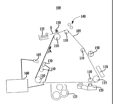
Figure 1 represents a block diagram of an electrophotographic image-
forming machine having an on-line pulse densitometer according to one
embodiment.
Figure 2 represents a block diagram of an on-line densitometer
according to one embodiment.
CA 02386136 2002-04-02
Figure 3 represents a chart of voltage signals used by an on-line
densitometer to measure density according to one embodiment.
DETAILED DESCRIPTION OF THE PREFERRED EMBODIMENTS
Figure 1 represents a block diagram of an electrophotographic (EP)
5 image-forming machine 100 with a pulse densitometer according to one
embodiment. A photoconductor 105 is operatively mounted on support rollers
110 and a motor driven roller 115, which moves the photoconductor 105 in the
direction indicated by arrow A. A primary charger 118, an exposure machine
120, a toning station 125, a transfer charger 130, a fusing station 140, and a
cleaner 150 are operatively disposed adjacent to the photoconductor 105. A
densitometer 160 has an emitter 165 and a collector 170, which are
oppositely positioned across the photoconductor 105. In one aspect, the
photoconductor 105 has a belt and roller-mounted configuration. However,
the photoconductor 105 may be mounted using a drum or other suitable
configuration. While a particular configuration and arrangement are shown for
the EP image-forming machine 100, the invention may use other
configurations and arrangements including those with additional or fewer
components.
Figure 2 represents a block diagram of the densitometer 160 according
to one embodiment. The emitter 165 may be an infrared emitting diode
(IRED) connected to a resistor 175 and a pulse oscillator 180. The emitter
also may be a light emitting diode (LED). In one aspect, the emitter 165 is
current limited by the resistor 175 and is driven by the pulse oscillator 180.
The collector 170 is connected to an operational amplifier 185, which has a
resister 195 forming a feedback loop. The collector 170 may be a silicon
photodiode or other photodiode. The densitometer may be a transmission
densitometer, a reflection densitometer, or other density measurement device.
While a particular pulse apparatus and arrangement are described for
the pulse oscillator 180, other pulse apparatus and arrangements may be
used to provide the duty cycle of the densitometer for the film. The emitter
CA 02386136 2002-04-02
6
165 also may have a blocking device or shutter (not shown) that blocks and
unblocks emissions from the emitter 165 in response to the duty cycle.
The emitter 165 and the collector 170 may be configured to operate
with the type of film used on the photoconductor 105. By pulsing the emitter
165 below the exposure threshold of the film, the amount of emissions from
the emitter 165 may not result in a significant exposure of the film even
though the film may have infrared or color sensitivity. The film may be any
film used in electrophotographic image-forming machines. The film may be
sensitive to the wavelength of the emitter 165. The film may be sensitive to
color (visible light), the infrared spectral region, and other electromagnetic
emissions.
The duty cycle, wavelength, and other features of the emitter 165 and
collector 170 may be selected to avoid artifacts on the film. While particular
configurations are described below including particular wavelengths and duty
cycles, other configurations with other wavelengths and duty cycles may be
used to prevent artifacts.
The emitter 165 may have any wavelength as long as the emissions
may be provided essentially below the exposure threshold of the film. In one
aspect, the wavelength of the emitter 165 is selected depending upon the
length of the pulses or duty cycle. In another aspect, higher wavelength
emitters (not shown) are used with longer pulses or higher duty cycles. The
emitter 165 may be made of GaAIAs or any other suitable material.
In this embodiment, the emitter 165 is an infrared emitting diode
(IRED). The emitter 165 may have a wavelength equal to or greater than
about 880 nm. In one aspect, the wavelength of the emitter is in the range of
about 940 nm through about 950 nm. The emitter 165 also rnay have a
shorter wavelength, even in the visible light range. If in the visible light
range,
the emitter 165 may be a light emitting diode (LED).
In this embodiment, the pulse osallator 180 and amplifier 185 are
connected to a sample-and-hold (SlH) circuit 190, which may be an integrated
circuit (IC). The SlH circuit 190 may be connected to a control device (not
shown) such as the logic and control unit (LCU) or other microprocessor of
CA 02386136 2002-04-02
7
the EP image-forming machine 100. The SIH circuit 190 provides a voltage
reading to the LCU corresponding to the density of the area read on the
photoconductor 105.
In use, the emitter 165 emits pulses in response to a drive signal
generated by the pulse oscillator 180. The drive signal activates and
deactivates the emitter 165 according to the duty cycle. The collector or
photodiode 170 is active, and may be always active, to receive incoming
pulse emissions from the emitter 165. The photodiode 170 receives the
pulses passing through the photoconductor 105. The amplifier 185 provides
an amplified output signal to the SIH circuit 190 in response to the pulses
received by the photodiode 170. The amplified output signal corresponds to
the density of the photoconductor 105 and any toner. In one aspect, the
density of a process patch (not shown) is measured. Other areas and
densities also may be measured.
The operation of the emitter 165 may be synchronized with the
operation of the S/H circuit 190. There may be time lags at the start of a
pulse associated with activating the drive signal, starting the pulse emission
and reception, and generating the amplified output signal. These time lags
occur during a ramp-up period following the start of the drive signal or
pulse.
Similarly, there may be time lags at the end of a pulse associated with
deactivating the drive signal, ending the pulse emission and reception, and
ending generation of the amplified output signal. These time lags occur
during, a ramp-down period following the end of the drive signal or pulse. The
presence of the amplified output signal during the ramp-up and ramp-down
periods may lessen the accuracy of the density reading. To reduce or
eliminate the effect of the ramp-up and ramp-down periods on the density
readings, the pulse oscillator 180 provides a synchronization signal to the
SIH
circuit 190. The synchronization signal properly times the pulses from the
emitter 165 with a hold function of the S/H circuit 190.
Figure 3 represents a chart of voltage signals used by an on-line
densitometer to measure density and shows the synchronization of the emitter
165 and the SIH circuit 190 according to one embodiment. The pulse
CA 02386136 2002-04-02
8
oscillator 180 generates a drive signal to measure a first density D~. The
drive
signal causes the emitter 165 to emit a pulse during time period T~. The
collector or photodiode 170 receives the incoming pulse emission, thus
providing an amplified output signal 301 from the amplifier 185 to the S/H
circuit 190. The voltage level of the amplified output signal 301 may be a
function of density. In one aspect, the amplified output signal 301 is
inversely
(elated to the density. In this aspect, a higher voltage level is less dense
than
a lower voltage level. In other words, as density increases (as sensed by the
light received by the collector 170) the voltage level decreases.
Responsive to the synchronization signal from the pulse oscillator 180,
the SIH circuit 190 takes a sample of the amplified output signal 301 during a
sample period T3 to obtain a hold signal 302. The sample period T3 is after
the ramp-up period T2, but before the ramp-down period T4. The hold signal
302 during sample period T3 corresponds to the first density D~.
The SIH circuit 190 provides an SIH output signal 303 to the LCU. The
SIH circuit holds the SIH output signal 303 at the hold signal 302 taken
during
time period T3 until the next density measurement is taken. The density
measurement of the second density DZ is taken in the same manner as the
density measurement of the first density D~. The second density D2 may be
lower than the first density D~ (i.e., the amplified output signal 301 has a
higher voltage at DZ than at D~). Accordingly, the S/H output signal is higher
for the second density D2 than the first density D~. The S/H circuit 190 holds
the S/H output signal 303 at this higher level until the next density
measurement. White the second density D2 is shown lower than the first
density D~, the second density DZ may be higher than the first density such as
when the photoconductor has the maximum amount of toner. The S/H output
signal 303 may decrease and may reach about zero volts. The duty cycle
also may control the timing of the density measurements for the first and
second densities D~ and D2.
The duty cycle represents the time duration of a pulse from the emitter
165. The duty cycle may be selected depending upon the spectral response
of the film on the photoconductor 105. Each film has an exposure threshold,
CA 02386136 2002-04-02
9
which includes the length of time when a pulse starts to produce or produces
an artifact or fogs an image on the film. In one embodiment, the duty cycle is
lower than the exposure threshold of the film. In ane aspect, the duty cycle
is
equal to or less than about five percent.
In addition, the duty cycle may be selected depending upon the
°settling time" of the S/H circuit 190. The settling time is the length
of time
required for the S/H circuit 190 to obtain a suitable hold signal 302. The
settling time includes the ramp-up time T2 and the sample time T3, and may
also include the ramp-down time T,,. The ramp-up time T2 may be reduced or
substantially eliminated by the selection of appropriate components for the
densitometer 160 such as the emitter 165, the collector 170, the amplifier
185,
and others. With an appropriate selection of components, the settling time
may be essentially the same as the sample time T3. In addition, the sample
time T3 also may be reduced with the appropriate component selection. The
duty cycle may be equal to or greater than the settling time. In one aspect,
the duty cycle is equal to or greater than one percent.
The duty cycle may be in the range of about one percent through about
five percent. When the emitter 165 is an infrared emitting diode (IRED), the
temperature increase of the IRED 165 may not be significant within that
range. The duty cycle may be preset by instructions in the S/H circuit 190, a
microprocessor, or a control device such as the LCU. The duty cycle may be
adjustable, set and changed, by the SIH circuit 190, the LCU, another
microprocessor, and the like. With an adjustable duty cycle, the EP image-
forming machine 100 may use different kinds of film.
Various embodiments of the invention have been described and
illustrated. However, the description and illustrations are by way of example
only. Many more embodiments and implementations are possible within the
scope of this invention and will be apparent to those of ordinary skill in the
art.
Therefore, the invention is not limited to the specific details,
representative
embodiments, and illustrated examples in this description. Accordingly, the
invention is not to be restricted except in light as necessitated by the
accompanying claims and their equivalents.