Note: Descriptions are shown in the official language in which they were submitted.
CA 02386172 2004-12-16
1
PATTERNED LAMINATES AND ELECTRODES WITH
LASER DEFINED FEATURES
BACKGROUND OF THE INVENTION
The present invention relates to laser ablation to pattern a metallic layer,
as
well as an electrode for an electrochemical biosensor.
Electrochemical biosensors are well known. They have been used to
determine the concentration of various analytes from biological samples,
particularly
from blood. Electrochemical biosensors are described in U.S. Patent
Nos. 5,413,690; 5,762,770 and 5,798,031; as well as in International
Publication
No. W099/13101.
An electrochemical biosensor typically includes a sensor strip. The sensor
strip includes a space that holds the sample to be analyzed, may include
reagents to
be released into the sample, and includes an electrode set. The electrode set
normally includes an insulating substrate, electrodes that contact the sample,
which
have contact pads for electrically connecting the electrodes to the
electronics of
electrochemical biosensor.
It is desirable for electrochemical biosensors to be able to analyze
electrolytes using as small a sample as possible, and therefore it is
necessary to
miniaturize the sensor strip, as well as its parts, including the electrodes,
as much as
possible. Usually screen printing techniques have been used to form
miniaturized
electrodes.
Electrodes formed by screen printing techniques can only be formed from
composition that are both electrically conductive and which are screen
printable.
Furthermore, screen printing techniques only allow for the reliable formation
of
structures and patterns having a feature size of approximately 75 pm or
greater. In
addition, screen printing is a wet chemical process. It would be desirable to
have a
new method of forming electrodes which allows for the use of different
composition,
and which can form features smaller than 75 Vim.
CA 02386172 2004-12-16
2
Laser ablation is a technique using a laser to cut or mold a material. This
technique usually uses a high power excimer laser, such as a krypton-fluoride
excimer laser with an illumination wavelength of 248 nm, to blast away surface
material. This technique has been used to ablate metals, polymers and even
biological material, such as the cornea of the human eye. Such systems are
well
known to those of ordinary skill in the art, and are described in U.S. Patent
Nos. 5,576,073 and 5,593,739.
SUMMARY OF THE INVENTION
In one aspect, the invention is a method of making a patterned laminate
comprising ablating through a portion of a metallic layer with a laser. The
metallic
layer comprises at least one member of gold, platinum, palladium and iridium.
Furthermore, the metallic layer is on, and in contact with, an insulating
substrate, for
example, a polymer.
In another aspect, the invention is a method of making a electrode set,
comprising ablating through a portion of a first metallic layer with a laser,
to form an
electrode pattern. The first metallic layer is on an insulating substrate.
In still another aspect, the invention is a method of making an electrode set
ribbon, comprising ablating through a portion of a first metallic layer with a
laser, to
form a plurality of electrode patterns. The first metallic layer is on an
insulating
substrate, for example, a polymer. The electrode set ribbon comprises a
plurality of
electrode sets.
In yet another aspect, the present invention is an electrode set, comprising a
first metallic layer, on an insulating substrate, comprising a plurality of
electrodes.
The first metallic layer has a feature size of less than 75 ~.m.
In yet another aspect, the present invention is a patterned laminate,
comprising a patterned metallic layer on, and in contact with, an insulating
substrate.
The metallic layer comprises at least one of gold, platinum,
CA 02386172 2002-03-28
WO 01/25775 PCT/LTS00/27197
3
palladium and iridium. Furthermore, the insulating substrate comprises a
polymer, and the patterned metallic layer has a feature size of less than
75 Vim.
An advantage of the present invention is that it allows for the possibility
of small feature sizes.
As used herein, the phrase "patterned laminate" means a multilayered
structure that includes an overlayer through which an underlying layer is
exposed, i.e. the overlayer has gaps and does not completely cover the
underlying layer. The gaps or areas of exposure form the "pattern" of the
patterned laminate. Furthermore, the term "pattern" means one or more
intentionally formed gaps having a feature size, for example, a single linear
gap having a constant width, where the smallest width is the feature size. Not
included in the term "pattern" are natural, unintentional defects.
As used herein, the phrase "feature size" is the smallest dimension of a
gap found in a pattern.
As used herein, the phrase "electrode pattern" is a pattern which when
formed in a metallic layer includes at least two, for example 2 to 60, or 3 to
20,
electrodes which are not electrically connected to each other, but each of
which includes its own contact pad.
As used herein, the phrase "metallic layer" refers to a layer made of a
material that is a metallic conductor of electricity, such as a pure metal or
alloys.
As used herein, the phrase "electrode set" is a set of at least two
electrodes, for example 2 to 60, or 3 to 20, electrodes. These electrodes may
be, for example, a working electrode and a reference electrode.
As used herein, the phrase "ablating" means the removing of material.
Other objects, features and advantages of the present invention will
become apparent from the following detailed description. It should be
understood, however, that the detailed description and the specific examples,
while indicating embodiments of the invention, are given by way of
illustration
only, since various changes and modifications within the spirit and scope of
CA 02386172 2004-12-16
4
the invention will become apparent to those skilled in the art from this
detailed
description.
In accordance with one aspect of the present invention there is a method of
making an electrode set comprising: ablating through a portion of a first
metallic layer
with a laser, to form, an interlacing electrode pattern defining said
electrode set;
wherein said first metallic layer is on a flexible insulating substrate.
In accordance with another aspect of the present invention there is a method
of making an electrode set ribbon, comprising: ablating through a portion of a
first
metallic layer with a laser, to form a plurality of electrodes with an
interlacing pattern;
wherein said first metallic layer is on a flexible insulating substrate; and
said
electrode set ribbon comprises a plurality of electrode sets.
In accordance with yet another aspect of the present invention there is an
electrode set, comprising a first metallic layer on a flexible insulating
substrate,
wherein a portion of the first metallic layer is laser ablated and in an
interlacing
electrode pattern.
In accordance with a further aspect of the present invention there is an
electrode set ribbon, comprising a first metallic layer on a flexible
insulating
substrate, wherein a portion of the first metallic layer is laser ablated and
in an
interlacing electrode pattern.
In accordance with one embodiment of the present invention there is an
electrode set, comprising: a first metallic layer, on a flexible insulating
substrate,
comprising a plurality of electrodes with an interlacing electrode pattern,
wherein said
first metallic layer has a feature size between said electrodes of less than
75 Nm.
In accordance with another embodiment of the present invention there is a
sensor strip, comprising: an electrode set having a first metallic layer on a
flexible
insulating substrate, wherein a portion of the first metallic layer is laser
ablated, and
the electrodes having contact pads, which are electrically connected to a
sensing
region of the electrodes.
CA 02386172 2004-12-16
4a
In accordance with yet another embodiment of the present invention there is
packaged sensor strips, comprising; a plurality of the sensor strips, a vial,
containing
said plurality of said sensor strips, and a stopper, sealing said vial, the
sensor strips
each including electrodes having contact pads, which are electrically
connected to a
sensing region of the electrodes, wherein each sensor strip comprises: an
electrode
set prepared by ablating through a portion of a first metallic layer with a
laser wherein
the first metallic layer is on a flexible insulating substrate, and the
electrodes having
contact pads, which are electrically connected to a sensing region of the
electrodes.
BRIEF DESCRIPTION OF THE DRAWINGS
The following drawings form part of the present specification and are included
to further demonstrate certain aspects of the present invention. The invention
may
be better understood by reference to one or more of these drawings in
combination
with the detailed description of specific embodiments presented herein:
Figure 1 illustrates an electrochemical sensor strip of the present invention;
Figure 2 illustrates an exploded view of an electrochemical sensor strip of
the
present invention, more clearing show each individual part;
Figure 3 illustrates an electrode set of the present invention;
Figure 4 illustrates another electrode set of the present invention;
Figure 5 illustrates still another electrode set of the present invention;
Figure 6 is a schematic of still another electrode set of the present
invention;
Figure 7 is a schematic of an electrode set ribbon of the present invention;
Figure 8 is a schematic of a device of the present invention for making an
electrode set ribbon of the present invention; and
Figure 9 is a block diagram of a process of the present invention for making a
sensor strip of the present invention.
CA 02386172 2004-12-16
4b
DETAILED DESCRIPTION OF THE INVENTION
Figure 1 illustrates the assembled electrochemical sensor strip 12, which
includes a base 1, the contact pads 9 and 9 that are part of the electrodes.
The
sensing region 10 of the electrodes is also illustrated.
Figure 2 illustrates an exploded view of a sensor strip 12, which includes a
base 1, adhesive foil 2 for holding the base to the electrode
CA 02386172 2002-03-28
WO 01/25775 PCT/US00/27197
substrate 3. The electrode set 16 is on the electrode substrate 3, and is
partially covered by a dielectric 5. A cover 8 is attached to one end of the
dielectric with adhesive tape 7. A small gap 13 in the dielectric, and a
space 14 in the adhesive tape, together with the cover and the electrodes,
5 form a pocket inside of which may be place reagent 6 used to aid in electro-
chemically detecting and quantifying an analyte. This pocket can act as a
capillary, drawing the fluid to be tested onto the sensing region 10 (not
shown)
of the electrodes. Alternatively, the cover may be absent, exposing the
sensing region of the electrodes, and the sample may be directly applied onto
this region.
Figure 3 illustrates an electrode set 16, including two electrodes 4 and
4. The electrodes have contact pads 9 and 9, which are electrically
connected to the sensing region 10 of the electrode. Also illustrated is
dielectric 5 which covers the first and second electrodes, exposing only the
sensing region and the contact pads.
Figures 4 and 5 illustrate two different electrode sets 16, which each
include a substrate 1, and first and second electrodes 4 and 4. The
electrodes are separated by a gap 18 that prevents electrical contact between
the two electrodes. For purposes of illustration, the regions of the
electrodes
which will become the sensing region 10, and the contact pads, 9 and 9, are
shaded. The gap 18 corresponds to the feature size of this electrode set,
since it is the smallest intentional feature. Figures 4 and 5 illustrate two
different electrode patterns, one having a simple straight gap (Figure 4), and
the other more complex and containing a rectilinear gap, forming a region of
interlacing fingers of the two electrodes (Figure 5).
Figure 6 is a schematic of an electrode set of the present invention,
including two electrodes 4 and 4. The sensing region 10 of the electrodes
contains interlacing fingers of the two electrodes, again a rectilinear gap.
Also
shown opposite the sensing region are the contact pads 9 and 9 of each
electrode. The gap between the electrodes corresponds to the feature size,
and may be 1 to 100 Vim, preferably less than 75 Vim, more preferably 5 to
50 Vim, most preferably 10 to 30 Vim. The gap passes completely through the
CA 02386172 2002-03-28
WO 01/25775 PCT/US00/27197
6
metallic layer so that the two electrodes are not electrically connected in
the
electrode set. The values for the dimensions illustrated in Figure 6 are for a
single specific embodiment, and these values may be selected as need for
the specific use. For example, the length of the electrode set may be 2.5 to
250 mm, the width may be 0.4 to 40 mm, the gap between the contact pads
may be 1 ~m to 5 mm, and the width of each contact pad may be 1 to 20 mm
The electrode pattern shown in Figure 6 (and other figures) is symmetric,
however this is not required, and irregular or asymmetric patters (or
electrode
shapes) are possible.
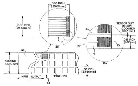
Figure 7 is a schematic of an electrode set ribbon 24. The ribbon
includes a plurality of panels 20, each of which includes a plurality of
electrode sets 16. Also shown is the original metallic laminate ribbon 22 that
is subject to laser ablation to form the electrode set ribbon 24. The width of
the ribbon is selected to accommodate the laser ablation system, and may be,
for example, 40 to 0.4 inches. The ribbon may be any length, and is selected
based on the desired number of electrode sets, and/or the ease of handling
and transport of the ribbons. The size of each individual panel is selected to
fit conveniently on the ribbon, and therefore each panel may contain 1 to 1000
electrode sets, preferably 2 to 20 electrode sets.
Figure 8 is a schematic of a device for producing electrode sets, in the
form of an electrode set ribbon 24. First a roll of metallic laminate ribbon
22 is
fed through guide rolls 28 into a laser ablator 26. In the laser ablator the
metallic layer of the metallic laminate ribbon is ablated with the laser, in
an
electrode pattern, to form the electrode set ribbon 24. The electrode set
ribbon 24 is then passed through more guide rolls 28, with a tension loop to
adjust the tension of the ribbon, and through an optional inspection
camera 30, which may be used to check for defects. Next, optionally, the
electrode set ribbon 24 may be laminated with an adhesive foil ribbon 32, in a
laminator 36, to form a laminated electrode set ribbon 34, which is then
guided through guide rolls 28, and rolled up.
Figure 9 is a block diagram of a process for making an electrochemical
sensor strip of the present invention. As shown, in step 110 the metallic
CA 02386172 2002-03-28
WO 01/25775 PCT/US00/27197
7
laminate ribbon 22 is ablated by laser ablation to form an electrode set
ribbon,
and then laminated with adhesive foil ribbon 32 to form a laminated electrode
set ribbon 34. In step 120 the laminated electrode set ribbon 34 is screen
printed with a UV curable dielectric 50, which forms the dielectric 5 (not
shown) of each sensor strip, forming a dielectric covered ribbon 38. In
step 130 the starting reagents 40 are compounded to form reagent 6, and
then in step 140 the reagent is applied onto the dielectric covered ribbon 38,
the ribbon is split into reels, each one panel wide, to form reagent covered
panel reels 44.
In step 150 the reagent covered panel reels 44 are covered with clear
polyester roll 52 attach through double sided adhesive tape roll 54, which
forms the clear cover 8 (not shown) and adhesive tape 7 (not shown) of each
sensor strip. The product of step 150, clear covered panel reels 46, are then
split into individual sensor reels, each one electrode set wide, and laminated
with a base substrate roll 56, in step 160, which forms the base 1 (not shown)
of each sensor strip, to form sensor reels 48. In step 170 the sensor reels
are
cut into individual sensor strips 12 (not shown) which are sorted and packed
into vials 60, each closed with a stopper 58, to give packaged sensor
strips 62. In steps 150 and 160, a liner is release in order to attach the
base
and cover.
A laser system capable of ablating the metallic layer, to form the
individual electrode sets, is well known to those of ordinary skill in the
art.
Examples include excimer lasers, with the pattern of ablation controlled by
lenses, mirrors or masks. An example of such a system is the LPX-400, or
LPX-200, both from LPKF LASER ELECTRONIC, GMBH of Garbsen,
Germany.
The metallic laminate is a metallic layer on the electrode substrate.
The metallic layer may contain pure metals or alloys, or other materials which
are metallic conductors. Examples include aluminum, carbon (such as
graphite), cobalt, copper, gallium, gold, indium, iridium, iron, lead,
magnesium, mercury (as an amalgam), nickel, niobium, osmium, palladium,
platinum, rhenium, rhodium, selenium, silicon (such as highly doped
CA 02386172 2004-12-16
8
polycrystalline silicon), silver, tantalum, tin, titanium, tungsten, uranium,
vanadium,
zinc, zirconium, mixtures thereof, and alloys or metallic compounds of these
elements. Preferably, the metallic layer includes gold, platinum, palladium,
iridium, or
alloys of these metals, since such noble metals and their alloys are
unreactive in
biological systems. The metallic layer may be any thickness, but preferably is
10 nm
to 1 mm, more preferably, 20 nm to 100 Vim, or even 25 nm to 1 pm. Figure 9
illustrates the process with a 50 nm gold film.
In the laser ablation process, the metallic layer may be ablated into an
electrode pattern. Furthermore the patterned metallic layer may be coated or
plated
with additional metal layers. For example, the metallic layer may be copper,
which is
then ablated with a laser, into an electrode pattern; subsequently, the copper
may be
plated with a titanium/tungsten layer, and then a gold layer, to form the
desired
electrodes. Preferably, however, only a single layer of gold is used, which is
directly
in contact with the electrode substrate, since it allows for the entire
elimination of wet
chemical steps for the formation of the electrode sets.
The electrode substrate is formed from an insulating material, so that it will
not provide an electrical connection between the electrodes of the electrode
set.
Examples include glass, ceramics and polymers. Preferably, the electrode
substrate
is a flexible polymer, such as a polyester or polyimide. An example of a
suitable
material would be the polyimide UPLEXTM from TECHNI-MET of Connecticut, which
is available pre-coated with gold, palladium or platinum; or ULTEMTM 1000
(polyetherimide) from GE, available coated with copper.
A UV curable dielectric and which is screen printable, may be used to form
the dielectric, for example the polymer composition 5018 dielectric
composition from
DuPontT"". The clear cover is a clear material that is inert to biological
fluids, for
example glass, polyethylene, polypropylene, polyvinylchloride, polyimide, or
polyester. The clear cover may have markings. The adhesive tape is also a
flexible
polymer having a surfaces
CA 02386172 2004-12-16
9
covered with an adhesive; these materials are also well known to those of
ordinary
skill in the art.
The base is a supporting structure, and is preferably made of flexible polymer
material, with a thickness sufficient to provide support to the sensor strip,
for example
polyester with a thickness of 6 mils. The adhesive foil may be made for the
same
types of compositions as the adhesive tape.
The reagent is optional, and may be used to provide electrochemical probes
for specific analytes. The starting reagents are the reactants or components
of the
reagent, and are often compounded together in liquid form before application
to the
ribbons or reels. The liquid may then evaporate, leaving the reagent in solid
form.
The choice of specific reagent depends on the specific analyte or analytes to
be
measure, and are well known to those of ordinary skill in the art. For
example, a
reagent for measurement of glucose in a human blood sample contains 62.2 mg
polyethylene oxide (mean molecular weight of 100-900 kilodaltons), 3.3 mg
NATROSOLTM 250 M, 41.5 mg AVICELTM RC-591 F, 89.4 mg monobasic potassium
phosphate, 157.9 mg dibasic potassium phosphate, 437.3 mg potassium
ferricyanide, 46.0 mg sodium succinate, 148.0 mg trehalose, 2.6 mg TRITONT"" X-
100 surfactant, and 2,000 to 9,000 units of enzyme activity per gram of
reagent. The
enzyme is prepared as an enzyme solution from 12.5 mg coenzyme PQQ and 1.21
million units of the apoenzyme of quinoprotein glucose dehydrogenase, forming
a
solution of quinoprotein glucose dehydrogenase. This reagent is described in
WO
99!30152, pages 7-10.
The processes and products described include disposable biosensors,
especially for use in diagnostic devices. However, also included are
electrochemical
sensors for non-diagnostic uses, such as measuring an analyte in any
biological,
environmental, or other, sample. Furthermore, also included is any patterned
laminate, preferably a patterned laminate of a noble metal (gold, platinum,
palladium,
iridium, alloys thereof) in direct contact with an insulating substrate, such
as a
polymer. Such laminates can have a variety of electrical function, including
use as
electrodes, electrical wires or connectors, microwave reflectors, etc.
Preferably,
these patterned laminates
CA 02386172 2002-03-28
WO 01/25775 PCT/US00/27197
have a feature size of 100 ~m or less, more preferably 1 to 100 Vim, even
more preferably 75 ~m or less, including 5 to 50 Vim, or even 5 to 20 Vim.