Note: Descriptions are shown in the official language in which they were submitted.
CA 02386348 2002-04-03
WO 01/53787 PCT/USO1/02013
FLEXIBLE FIBER OPTIC MICROBEND DEVICE,
SENSORS, AND METHOD OF USE
FIELD OF THE INVENTION
The present invention relates to fiber optic devices. In particular, it
relates to a
flexible microbend device that may be attached to an optical fiber and used in
a sensor
arrangement for measuring internal strain in a structure.
BACKGROUND OF THE INVENTION
Optical fibers are used to convey light between a light source and a light
detector. Light in the fiber can be modulated by bending or otherwise
distorting the
fiber. This produces a modulated signal which can be picked up and processed
by the
light detector.
Microbend devices may be used to induce distortions in a fiber causing the
light passing through the fiber to be modulated at a frequency corresponding
to the
force applied to the device. Typically, the device is applied to the fiber
such that it
surrounds the fiber.
One known device is a two jaw corrugated arrangement which squeezes an
optical fiber to modulate the light signal passing therethrough. Macedo et al.
(U.S.
4,342,907) describes such a device where an upper piece is firmly connected to
an
enclosure by a support. A lower piece was attached to an elastic membrane.
When
either a static pressure or dynamic time varying pressure reaches the
membrane, it
deflects pushing the lower piece, toward the upper piece, thus deforming the
optical
fiber which is held against the ridges of the device. They also describe
another
approach in U.S. 4,443,700 where two steel pieces having corrugated like
surfaces
with interleaving ridges form a vise which would be used to squeeze and thus
deform
the fiber. Such devices fail to have the compae;tness and flexibility desired
for
measuring forces internally in a structure.
CA 02386348 2002-04-03
WO 01/53787 PCT/USO1/02013
Kramer (U.S. 5,193,129) introduced microbends by interweaving an optical
fiber through rungs of a ladder-like structure, encapsulating it in a foam-
like material,
and surrounding it with a sheath. Light transmitted through the optical fiber
is
diminished to a value less than a threshold value upon the occurrence of
microbending
caused by pressure applied at any location along the length thereof. The rungs
of the
ladder structure are sized and spaced to provide a proper locus about which
microbending may be produced. Sansone (U.S. 5,694,497) points out one of the
deficiencies of this sensor by stating that it must use part of the structure
it is
embedded in to complete the sensor design. In fact, the utility of this type
of sensor is
limited in that it must be woven into the substrate or structure being
measured and
cannot be later repositioned as needed.
Udd et al. (U.S. 5,118,931) introduced microbends into their sensor system by
melting the optical fiber and pulling simultaneously to give the fiber a
smaller
diameter. Lengths of this fiber were spliced into the unmelted fiber to
produce the
sensor. Deformation of the fiber affects propagation of light therethrough,
permitting
detection based upon detected changes in light throughput. As with the Kramer
device, the deficiency in this design is that once spliced into the fiber,
there is no way
to later reposition the structure.
Sansone (U.S. 5,694,497) describes an intrinsically self deforming microbend
deformer. In this device, the fiber is twisted about itself. At least one
twisted section
acts as an intrinsically self deforming microbend deformer. The problem with
this
device is that there is no way to obtain a fixed period and/or thus be able to
adjust the
sensitivity of the sensor.
An object of the present invention is to provide a microbend device that may
2~ bz removed and reattached to an optical fiber along its length.
Another object of the present invention is to provide a microbend device that
is Fle,cible.
CA 02386348 2002-04-03
WO 01/53787 PCT/iJS01/02013
Another object of the present invention is to provide a sensor that employs a
flexible microbend device, such that the sensor is intensity-based.
Another object of the present invention is to provide a method for using a
sensor that employs a flexible microbend device, such that the method is used
to
measure either radial or linear forces.
SUMMARY OF THE INVENTION
By the present invention, a flexible microbend device for attachment to an
optical fiber is provided. The device comprises an upper bending element grid
having
at least one flexible element and a lower bending element grid having at least
one
flexible element. Each upper bending element grid alternately engages each
lower
bending element grid.
When the device is attached to an optical fiber, it forms a fiber optic
microbend sensor. The optical fiber is positioned between each flexible
element of
the upper bending element grid and each flexible element of the lower bending
element grid such that each flexible element alternates between the upper and
the
lower bending element grids.
In use, the sensor is either attached to a surface of a structure or embedded
in a
host material. Optical power is introduced to the microbend sensor and the
reflected
light is monitored with a detector.
Additional objects and advantages of the invention will be set forth in part
in
the description which follows, and in part will be obvious from the
description, or
may be learned by practice of the invention. The objects and advantages of the
invention will be obtained by means of instrumentalities in combinations
particularly
pointed out in the appended claims.
-3-
CA 02386348 2002-04-03
WO 01/53787 PCT/USO1/02013
BRIEF DESCRIPTION OF THE DRAWINGS
The accompanying drawings illustrate a complete embodiment of the
invention according to the best modes so far devised for the practical
application of
the principles thereof, and in which:
FIG. 1A is a top view of the upper bending element grid of the flexible
microbend device of the present invention.
FIG. 1B is a top view of the lower bending element grid of the flexible
microbend device of the present invention.
FIG. 2A depicts the assembly of the flexible microbend device.
FIG. 2B is a top view of the flexible microbend device when it is assembled.
FIG. 3 is a top view of a fiber optic microbend sensor.
FIG. 4 depicts a sensor array.
FIG. 5A depicts an optical arrangement for the fiber optic microbend sensor.
FIG. 5B depicts an alternative optical arrangement for the fiber optic
1 S microbend sensor.
FIG. 6 is side view of a fiber optic microbend sensor which is encapsulated
and embedded in a host material.
DETAILED DESCRIPTION OF THE PREFERRED EMBODIMENTS
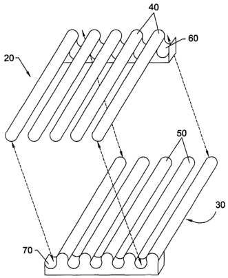
Referring now to the figures where similar elements are numbered the same
throughout, FIGS. IA and IB depict the flexible microbend device 10 of the
present
invention. For the purpose of this specification and the appended claims, by
flexible it
is meant that the device can undergo a deformation without breaking. Each
microbend device 10 comprises an upper bending element grid 20 and a lower
2~ bending element grid 3U. Although FIG. 1A depicts the upper bending element
grid
20 and FIG. 1 B depicts the lower bending element grid 30, the two may be
reversed.
Each bending element arid 2U, 3U, comprises at bast one tl~:cible element 40,
50.
Each upper flexible element 40 extends from an upper interlocking member 60,
-4-
CA 02386348 2002-04-03
WO 01/53787 PCT/IJSOl/02013
whereas each lower flexible element 50 extends from a lower interlocking
member 70.
FIGS. 1 A and 1 B depict a preferred embodiment where each bending element
grid 20,
30 comprises a plurality of bending elements 40, 50. However, the invention is
operable with the upper bending element grid having only one flexible element
and
the lower bending element grid having only one flexible element.
Each flexible element has a specific width, w, and diameter, d, and spaced
apart a certain distance to form a period A. The diameter of the flexible
element
influences the sensitivity of the device. It was found that the flexible
elements having
small diameters moved more easily than those of larger diameter. Each flexible
element has a stationery position at one end, or at the end where the flexible
element
is attacheu to the interlocking member, in order to establish a fixed period
A. The
period depends on whether the optical fiber used in the sensor is to be a
single mode
optical fiber or a multimode optical fiber. Preferably, the flexible element
is prepared
from a material selected from the group consisting of: a moldable plastic,
1 S micromachined silicon, an elastomer; and silica fiber. An example of
silica fiber is a
coated optical fiber which is cut to an appropriate length. The interlocking
members
are preferably prepared from a material selected from the group consisting of:
a
moldable plastic, micromachined silicon, and an elastomer. If micromachined
silicon
is used, v-grooves are etched into the silicon to from the interlocking
member.
FIG. 2A depicts how the upper bending element grid 20 is assembled with the
lower bending element grid 30 to form the flexible microbend device. The upper
bending element grid 20 has at least one upper interlocking member 60
positioned at
an end of each flexible element :10. Similarly, the lower bending element grid
30 has
at least one lower interlocking member 70 positioned at an end of each
flexible
2~ element 50. When engaged, each upper interlocking member 60 of the upper
bending
element grid 20 mates with each respective lower flexible element 50 of the
lower
bending element grid 3U such that tht lower tluxiblc clement 5U nests within
the upper
interlocking member 60. Similarly, each lower interlocking member 70 of the
lower
-5-
CA 02386348 2002-04-03
WO 01/53787 PCT/USO1/02013
bending element grid 30 mates with each respective upper flexible element 40
of the
upper bending element grid 20 such that the upper flexible element 40 nests
within the
lower interlocking member 70. This allows the upper bending element grid 20 to
be
secured to the lower bending element grid 30. The upper and lower interlocking
members 60, 70 are both depicted such that they are on the same side (or
bottom) of
the device when the device is assembled. However, it is understood that the
upper
interlocking member 60 could be positioned such that it is on a side opposite
from
(top side) the Lower interlocking member 70, which is on the bottom. Other
configurations suitable for the particular application of interest may be
used.
FIG. 2B depicts the flexible microbend device 10 after it has been assembled.
When the upper bending element grid 20 is engaged with the lo~.~er bending
element
grid 30, the flexible elements 40, 50 alternate. More specifically, the upper
flexible
element 40 is every other flexible element. Such an engagement is defined as
an
alternate engagement or where the upper bending element grid alternately
engages the
lower bending element grid.
FIG. 3 shows how the flexible microbend device 10 may be employed to form
a fiber optic microbend sensor. When forming the sensor, an optical fiber 80
is
positioned between each flexible element 40 of the upper bending element grid
20 and
each flexible element 50 of the lower bending element grid 30. Each flexible
element
40 of the upper bending element grid 20 alternately engages each flexible
element 50
of the lower bending element grid 30. Note that the optical fiber 80 is
sandwiched
between the upper and lower flexible elements, =40 and 50, as opposed to
weaving the
fiber between the flexible elements.
FIG. 4 shows how a sensor array 90 is formed by attaching a plurality of
2~ flexible microbend devices 14 to an optical fiber 80. Preferably, the array
is formed by
a single optical fiber passing through multiple flexible microbend devices.
However,
a plurality of optical fibers and fle;cible micrubend devices may be employed
to form
a three dimensional array or stack. In a typical application, one may have 21
flexible
-6-
CA 02386348 2002-04-03
WO 01/53787 PCT/USO1/02013
microbend devices attached to a single optical fiber within a thirty-foot
length. The
direction of sensitivity is orthogonal to the optical fiber. Either radial or
linear forces
are applied. As the force moves across the device, the top and bottom bending
elements move up and down changing the light intensity detected by the
detector.
The sensitivity may be varied by the flexible element diameter; by the number
of
flexible elements comprising the bending element grids; by adjusting the
period A, or
by changing the material properties of an encapsulating material.
The bending element grid has a stationery period. The periodic distance, A, is
calculated based on the type of optical fiber used for the sensor. If the
optical fiber is
a multimode optical fiber, the periodic distance, A, is defined by the
equation:
A = era
~~) ~2
0=n~Z-n~z
2n,~
where: a = radius of the core of the optical fiber
n, = core refractive index
n, = cladding refractive index.
When the optical fiber is a single mode optical fiber, the periodic distance,
A, is
lOpmsAs 1~OO~m. By adjusting the periodic distance, one can adjust the
sensitivity
of the sensor.
2~ As previously described, the flexible elements are preferably prepared from
a
material selected from the group consisting of: a moldable plastic;
micromachined
silicon; an elastumer; anc! silic;u libm. Whcn an ulastomcr is the choice
material,
preferably the elastomer is a polyurethane. As a further embodiment of the
invention,
CA 02386348 2002-04-03
WO 01/53787 PCT/USO1/02013
the sensor is encapsulated in a material having mechanical properties that are
different
from those of the flexible elements. For example, the encapsulated material
may be
selected from the group consisting of: silicone RTV; LTV-cured epoxy; an
elastomer;
and polyurethane. If the sensor is to eventually be embedded in a host
material, the
encapsulated material must be compatible with the host material. By host
material, it
is understood that the material may be a material surrounding a structure such
as the
rubber cover on a roller. Alternatively, the sensor may be encased in a
protective
covering, such as a vacuum bag.
FIG. 5A depicts one optical arrangement for the fiber optic microbend sensor.
The arrangement comprises an optical coupler 100 having a first end or lead
110
coupled to the optical fiber 80. A light source 120 is coupled to a second end
or Iea.d
130 of the optical coupler 100. A detector 140 is coupled to a third end or
lead 150 of
the optical coupler 100. A reflector 160 is positioned at an end of the
optical fiber 80
opposite from the light source 120.
FIG. 5B shows an alternate embodiment for the optical arrangement where a
fused, biconical, tapered device 210 is disposed between the optical coupler
100 and
the detector 140. The fused, biconical, tapered device 210 separates high and
low
order modes from an optical signal.
In one application, the fiber optic microbend sensor is attached to a surface
of
a structure. Optical power is introduced to the microbend sensor and reflected
light is
monitored with the detector. When the sensor is attached to the surface of a
structure,
the stress of force between two objects may be measured. In a second method,
shown
in FIG. 6, the fiber optic microbend sensor 170 is first encapsulated in a
material 180
and thin embedded in a host material 190, such as a rubber roller cover, that
2~ surrounds a structure 200. Optical power is introduced and the reflected
light is
monitored with the detector (not shown) as a force is applied to the roller.
In this
case, stress or strain on a material is detected.
_g_
CA 02386348 2002-04-03
WO 01/53787 PCT/USO1/02013
The above description and drawings are only illustrative of preferred
embodiments which achieve the objects, features and advantages of the present
invention, and it is not intended that the present invention be limited
thereto. Any
modification of the present invention which comes within the spirit and scope
of the
following claims is considered part of the present invention.
-9-