Note: Descriptions are shown in the official language in which they were submitted.
CA 02386352 2002-05-28
NxN Optical Matrix Switch Using Modified Cross-Connect of 1xN Switches
Technical Field
The present invention is an NxN optical matrix switch using a modified cross-
connection
of 1xN switches that are built with 2x2 switch units. The 2x2 switch units are
preferred to
be Mach-Zehnder interferometer type because it has two advantages of low power
consumption and low excess loss. It relates to a high-isolation, low insertion
loss, and
low-power-consumption optical switch for an optical communication system,
optical
interconnects, optical cross-connect, and a fiber-optic network system.
Background of the Invention
Today, the rapid development and applications of fiber-optic communication
systems
are stimulating various photonics networks based on some new microstructure
optoelectronic technologies instead of mechanical individual devices. Among
various
microstructure optoelectronic technologies, integrated optics represents a
promising
strategy in this field. One implementation of this strategy relies on the
integration of
optoelectronic interconnects on a host Si substrate, and thus requires
feasible
optoelectronic technologies in order to produce Si-based photonic devices. As
progress is
made on a variety of photonic networks, such as the optical cross-connects
(OXCs), the
dense wavelength division multiplexing (DWDM) and other kinds of optical
networks,
optical matrix switches are indispensable. These networks can provide flexible
operations
such as routing, restoration, and reconfiguration in the DWDM systems.
In long-haul transport networks, a hybrid technology is employed and traffic
is
transported optically, but most of operations are implemented as electronic
systems. The
switching and communication need to convert optical streams to electronic
signals and
then convert these signals to optical streams. The optical-electrical-optical
(0E0)
conversion based networks suffer from several inherent deficiencies such as
high cost,
lack of scalability and performance limitation. In local area networks,
optical switching is
an attractive candidate switching and communication. The optical matrix switch
is one of
most important components in constructing the photonic switching systems
including the
optical DWDM networks, the OXCs and mufti-channel testing systems. The maximum
number of subscribers will strongly depend on the properties of the individual
matrix
switches. The requirements for the implementation of such matrix switches in a
system
are low loss and low crosstalk. Furthermore, the switch points of the devices
should have
uniform switch characteristics and stable operating characteristics.
Most of optical switching devices in production today, typically the fiber-
optic
switches, use an opto-mechanical means to implement optical steering. This is
accomplished through the separation, or the alignment, or the reflection of
the light beam
by an opto-mechanical driven mirror. These designs offer good optical
performance such
as low insertion loss and reliable operation as well as mature technologies
for designing
and manufacturing, but have two typical drawbacks. One is slow speed. The
typical
settling times for switching are from lOms to 100ms. Even for some large-scale
optical
matrix switches, the setting times for switching are from 100's of
milliseconds to 1
second. The other disadvantage of the opto-mechanical switches is big size.
The
CA 02386352 2002-05-28
advantages of the fiber-optic switches based on the opto-mechanical
technologies come
from the use of direct or indirect fiber-to-fiber couplings, and the
disadvantages of this
type of optical switches come from the use of moving-parts. These
disadvantages,
however, could be acceptable in the conventional small-scale photonics
networks, but
today's high capacity communications really could not continue to suffer from
these out-
of age properties. To overcome some of these limitations, one selection is
taking the
advantages and overcoming the disadvantages of this type of optical switches,
and the
other selection is looking for other technical approaches that can support non-
mechanical
and no-moving-part optical matrix switches. Today, research and development of
optical
matrix switches have shown that the planar optical waveguides and the micro-
electro-
mechanical system (MEMS) are two promising technologies for developing
advanced
optical communication components in the near future.
The thermo-optic (TO) matrix switch and the electro-optic (E0) matrix switch
are two
promising planar waveguide optical switches for the future photonic switching
systems
and the reconfigurable optical interconnection of switching systems. For the
TO matrix
switches, the silica-based planar lightwave circuits (PLC's) is the most
promising
technical approach because it has lowest propagation loss, reliable
fabrication technique,
easy mass-production, polarization insensitivity, and easy interfacing with
fibers. The
nodes of the optical matrix switches are the 2x2 or 1x2 switch units. The TO
waveguide
devices using silica-on-silicon waveguides have shown an exciting advantage
over the
currently used mechanical and bulk optic devices in fiber-optic communications
because
of their great flexibility in fabrication and processing as well as speedy
operations than
the mechanical ones. The EO waveguide devices are generally based on diffused
LiNb03-based waveguides and have also presented a promising application in the
future
with its high-speed operation, low loss and mature manufacturing technology.
Basically there are two kinds of no-moving-part 2x2 optical waveguide
switches: one
uses the Mach-Zehnder interferometer (MZI) configuration and the other one is
digital
optical switch (DOS). 1x2 and 2x2 switches are basic units for building the
matrix
switches and the OXC systems. The former has two advantages: low power
consumption
and low access loss, and a disadvantage: wavelength sensitive. The latter has
two
disadvantages: high power consumption and high access loss, and an advantage:
wavelength insensitive. Thereby, the TO switch using the MZI configuration is
suitable
for low thermal coefficient (dn/dT) and high reliability material such as
PECVD-based
silica-on-silicon and EO switch using the MZI configuration currently uses the
LiNb03
diffused waveguides and will probably employ the reliable EO polymers in the
future. In
addition, the MZI configuration can also be used to build 2x2 fiber-optic
switches with
the fiber couplers.
Summary of the Invention
An NxN optical matrix switch using a modified cross-connection of 1xN switches
is
proposed in this invention where the 1xN switch unit is built with the
cascaded 2x2
switching nodes. In the NxN matrix switches, the operating speed, the device
size, the
complexity, the power consumption, the wavelength sensitivity, the insertion
loss, and
the blocking are main problems. In this invention, the optical outputs at the
OFF-state are
CA 02386352 2002-05-28
separated from the output ports at the ON-state where the switching operations
are
required, so the isolation between two adjacent channels can be greatly
improved.
Meanwhile, all the switching paths have to pass the same number of switching
units and
the same number of the activated switching units, so the high uniformity among
all the
optical paths can be achieved, and not only is a low power consumption
required for a
switching operation, but the same power consumption is needed for all the
switching
operations. Especially, in both the small-scale and the large-scale NxN matrix
switches,
this advantage is very apparent. As a result, the complexity, the insertion
loss and the
power consumption can be significantly reduced. This matrix switch structure
is proposed
based on physical approach where no-moving parts are included. Typically, the
optical
integrated circuits based on planar waveguide technology and the fiber-optic
networks
based on fiber technologies are two effective approaches. Thus the operating
speed of the
optical switches based on the present invention could be significantly
increased.
Generally there are two kinds of 2x2 waveguide optical switches: Mach-Zehnder
interferometer (MZI) switch and digital optical switch (DOS). The former has
two main
advantages: lower power consumption and lower access loss, and a main
disadvantage:
wavelength sensitive. The latter has a main advantage: wavelength
insensitivity and two
critic disadvantages: higher power consumption and higher access loss. The
power
consumption, the insertion loss and the wavelength sensitivity are three most
important
issues of an optical matrix switch. Therefore, the MZI type optical switch is
preferred to
use as a switching unit because it can directly meet two issues of the optical
matrix
switches with its two main advantages. Whereas, its disadvantage: wavelength
sensitivity
can be solved by another way in this invention as described above. If the
wavelength
sensitive 2x2 switching units such as MZI type optical switches are used as
the switching
units of the NxN optical matrix switch, at the different switching stages, the
2x2
switching units are designed at different central wavelengths to uniformly
cover the
whole wavelength range in this invention. So, the wavelength sensitivities
among all the
switching stages can be compensated for one another. Finally the performance
of NxN
optical matrix switch based on this invention includes low insertion loss,
high-speed
operation, low power consumption, wavelength insensitivity, compact device
size and
nonblocking.
In a desirable embodiment according to the present invention, 2N 1xN switches
are
used to form a nonblocking NxN matrix optical switch with a modified cross-
connection
where the 1xN switch is built with the cascaded 2x2 switches. In addition, the
two groups
of 1xN optical switches are specially distributed in one wafer to reduce the
device size
and complexity, and the MZI type switch is preferred and designed to work at
different
wavelengths to decrease the wavelength sensitivity of the whole NxN optical
matrix
switch based on this invention.
Brief Descriution of the Drawins
FIG. 1 is the configuration of an NxN optical matrix switch using the
magnified cross-
connect of 1xN switches where the 1xN switch is built with the cascaded 2x2
switching
nodes: (a) the top view and the construction of the NxN optical matrix switch
and (b) the
cross-section view.
CA 02386352 2002-05-28
FIG. 2(a) is the configuration of 1xN optical switch built with N-cascaded 2x2
Mach-
Zehnder switching nodes and FIG. 2{b) is of Nxl optical switch built with N-
cascaded
2x2 Mach-Zehnder switching nodes.
FIG. 3 is the configuration and operation principle of a 4x4 matrix optical
switch using
8 1x4 optical switch that is built with 4 cascaded 2x2 Mach-Zehnder switching
nodes: (a)
the complete construction and (b) an example of the operation principle.
FIG. 4 is the definition of the modified optical cross-connect network for the
NxN
matrix optical switch using the switching units.
FIG. 5 is the detailed structures of the Mach-Zehnder interferometer type 2x2
switch as
a switching unit or node having the inverse operations used in the present
invention: (a) is
based on the thermal-optic modulation and (b) the electro-optic modulation.
Detailed Description of the Invention
The matrix switches must be nonblocking, that means every input must have the
possibility to be interconnected to every output. In order to achieve this
point, a design of
matrix switch must meet a rearrangeable nonblocking network of permutation
nodes
involving the smallest possible number of switching units. Thus, a nonblocking
optical
matrix switch is a communication network between N input ports and N output
ports. In
fact, various communication networks have been studied and used for a long
time in the
conventional electrical communication systems. To build an optical nonblocking
communication between N input ports and N output pons directly using 2x2
switches as
units, there are several popular networks for nonblocking communications of
both
electrical and optical networks such as crossbar, perfect shuffle, crossover,
and butterfly.
The crossbar network needs different switching stages (from 2 to 2N) for the
nonblocking
communication between N input ports and N output ports among N channels, so
both the
insertion loss of devices and the power consumption for switching operation
are not
uniform and sometimes very high. The Links among the switching points,
however, are
simple and easy to be built with optical technique, so it is widely used in
today's optical
matrix switches. The latter three kinds of networks have a common advantage
that they
all only need .logz + 1 switching stages for the nonblocking communications
between N
input ports and N output ports, but this advantage is transparent only in
large-scale matrix
communication and the links among all the switching points are complex.
Another
interconnection structure in the nonblocking matrix communication is cross-
connection
between N 1xN switches and N Nxl switches wherein the main devices are 1xN or
Nxl
switches. Unlike opto-mechanical technology, the physical approaches having no
moving
parts such as the optical waveguide and fiber technologies are not easy to
directly form a
1xN or Nxl switching units, the sole approach is using the N-cascaded
structure of 2x2 or
1x2 switching units. The 2x2 or 1x2 switching units could be based on either
the MZI or
DOC configuration. In the present invention, a kind of nonblocking NxN optical
matrix
switches based on a modified one-stage optical cross-connect network between N
1xN
optical switches and N Nxl optical switches. Both the 1xN and Nxl optical
switches are
built with the N-cascaded 2x2 or 1x2 optical switches, and the MZI switching
units are
preferred in the optical matrix switches based on the present invention. With
this kind of
optical matrix structure, all the optical paths pass through the same number
of 2x2
switching units and the same number of switching units is activated for all
the switching
CA 02386352 2002-05-28
operations. So, not only is the insertion loss low and uniform, but the low
power
consumption is required for switching operations.
Figure 1 is the NxN optical waveguide matrix switch built with a modified one-
stage
optical cross-connection between N 1xN optical switches and N Nxl optical
switches
where Fig. 1(a) is the top view and Fig. 1(b) the cross-section view. This NxN
optical
matrix switch comprises a substrate 20, cladding 22, input switching units
24a, 24b, 24c
and 24d, output switching units 26a, 26b, 26c and 26d, waveguide links 28a,
28b, 28c
and 28d for connecting 24a-26a, 24b-26b, 24c-26c and 24d-26d, respectively,
electrodes
30a, 30b, 30c and 30d deposited on the input switching units and electrodes
32a, 32b,
32c and 32d on the output switching units. As shown in Fig. 1 (a), the
structure of the
NxN optical matrix switch based on this invention is divided into two areas:
one is
composed of N rows of 2x2 switching units and arranged in the upper site as
input area
and the other one is also composed of N rows of 2x2 switching units and
arranged in the
lower site as the output area. The switching units can be either the MZI or
the DOS 2x2
(or 1x2) optical switches, but the switching units must operate bar-state
switching at the
OFF-state (the unmodulated state) and the cross-state switching at the ON-
state (the
modulated state). In each row of switching units of the input area, N
switching units are
cascaded to form a 1xN optical switch, so N rows of switching units in the
input area
form N 1xN optical switches. In the same manner, in each row of switching
units of the
output area, N switching units are cascaded to form a Nx 1 optical switch, so
N rows of
switching units in the output area form N Nxl optical switches. Namely, 2 NxN
matrices
of switching units form the input area and the output area. As shown in Fig.
1, the input
switching units 24a through 24d are used to have the 1xN switching operations,
so the
electrodes 30a through 30d are required to make each switching unit have two
output
states. The output switching units 26a through 26d are used to have the Nxl
switching
operations, so the electrodes 32a through 32d are required to make each
switching unit
have two output states. Between the columns of the input area and the
corresponding
columns of the output area, there is a shift of one column in permutation so
that the
connection between the outputs of the switching units in the input area and
the inputs of
the switching units in the output area at the corresponding columns can be
easy with
cross-connect links 28a through 2$d. All the input ports of the input area are
labeled as
So , S, , through SN_, , and the output ports at the output area are labeled
as So , S; ,
through SN_, . While all the output ports of the input area are labeled as To
, T, , through
TN_1, and the input ports at the output area are labeled as To , T' , through
TN_1. As
mentioned above, each row of the input matrix is composed of N cascaded 2x2 or
1x2
switching units to form a 1xN optical switch and each row of the output matrix
is
composed of N cascaded 2x2 or 1x2 switching units to form an Nxl optical
switch as
shown in Fig. 2(a) and Fig. 2(b), respectively. For a 1xN optical switch based
on the
present invention, as shown in Fig. 2(a), one input port can have N+1 output
ports: one
output port is the other end of the cascaded switching units line and the
other N output
ports are formed by the N switching units 24a through 24d and labeled as 34a
through
34d. When an optical signal 38 is launched into the input port S , it can pass
through all
N cascaded switching units 24a through 24d and exits at the other end T of the
N
cascaded switching units line if no optical switching unit is activated by a
modulating
CA 02386352 2002-05-28
process. Once one of the optical switching units 24a through 24d is activated
by a
modulating process, this optical signal 38 can exit at the expected output
port of the
activated switching unit to form an optical output signal 40. Note that the
output end of
the N-cascaded switching units line is not used as switching operations, but
it can be used
to test the performance of the lx:h1 optical switch at the OFF-state. That is
why it is
labeled as T . For an Nxl optical switch based on the present invention, as
shown in Fig.
2(b), N+1 input ports correspond one output port. One input port is the input
end of the
N-cascaded switching units line and it is never used for the Nxl switching
operations, but
it can also be used to test the optical performance of the Nx 1 optical switch
at the OFF-
state, so it is labeled as T~ to match the output end S~ of the N-cascaded
switching units
line. The other N input ports are provided by the N switching units 26a
through 26d and
labeled as 36a through 36d. No matter which input port is used to launch an
optical
signal 42, it can not enter the N-cascaded switching units line and can only
go to the
unused output port (or called idle part) of the 2x2 switching unit where it is
launched.
But, when a 2x2 switching unit is activated by a modulating process, it is
immediately
switched to the output port of the 2x2 switching unit that is connected to the
N-cascaded
switching units line and can pass through all left switching units of the line
and exits at
the only output end S~ of the N-cascaded switching units line to form the
output optical
signal 44. As shown in Fig. 1, in the NxN optical matrix switches based on the
present
invention, any optical communication between one input port and one output
port is the
path selection of the optical signal through a 1xN operation and an Nxl
operation, so all
the path selections of optical signals between the N input ports and the N
output ports
pass the same number of the switching units (N+1) and the same number of
switching
units (2) is required to be activated for a switching operation. Even all the
optical paths
are almost same. Consequently, this kind of NxN optical matrix switches based
on the
present invention at least have two extra advantages in performance as well as
bi-
directional and nonblocking communication: 1) the uniform optical performance
and 2)
the lower power consumption, both of which are important issues for a matrix
optical
switch. Figure 3 illustrates an NxN optical matrix switch using a modified
optical cross-
connection between N 1xN optical switching units and N Nxl optical switching
units as
depicted in this invention when N=4. In other words, a 4x4 optical matrix
switch is built
by using the modified optical cross-connection between 4 1x4 optical switching
units and
4 4x1 optical switching units. Figure 3(a) shows the linking construction of
the modified
optical cross-connection between 4 1x4 optical switches and 4 4x1 optical
switches for
building the 4x4 optical matrix switch based on this invention when the switch
is at the
OFF-state and Figure 3(b) shows the operating principle of the 4x4 matrix
optical switch
with an operating sample. The input ports of the input area are So , S, , S2
and S3 , and
the output ports of the output area are Sa , S; , SZ and S3 . In the same
manner, the output
ports of the input area are To , T, , T2 and T3 , and the input ports of the
output area are To ,
T,~ , Ti and T3 . The four columns of switching units 24a, 24b, 24c and 24d in
the input
area and the four columns of switching units 26a, 26b, 26c and 26d in the
output area are
arranged as two matrices, so the input area and the output area are called
input and output
matrices, respectively. These two matrices are connected by the links 28a,
28b, 2$c and
28d. If the four optical signals 46a, 46b, 46c and 46d are launched into four
input ports:
~"~ .....~.-.._-,.,.,-..~.....
CA 02386352 2002-05-28
So , S, , SZ and S3 , respectively, as shown in Fig. 3(a), every signal can
pass through the
4 cascaded switching units of the row where they are launched and exit at
their own
output ports To , T, , T2 and T3 , respectively, at the OFF-state, i.e., no
modulating effects
are applied onto these switching units. Note from Fig. 3(a) that all the
optical signals
must be coming out from the output ports of the input area if no modulating
effect
applied onto the switching units. So, as shown in Fig. 3(b), for any switching
operation,
its linking path of an optical signal from one input port to one output port
of the matrix
optical switch must be built up based on the modulating effect applied onto
one switching
unit of the input matrix and one switching unit of the output matrix for
switching
operations. For example, as shown in Fig. 3(b), if the switching units having
shadows
indicate the modulated state, i.e., the first switching unit from top of units
24a and the
first switching unit from top of units 26a, the optical signal 46a launched
into the input
port So of this 4x4 optical matrix switch will be coming out at the output
port SN_,. As
depicted in Fig. 3(b), the operating process has been marked with the bigger
lines. The
same optical signal 46a can also have other output choices by modulating
different pair
of switching units in the input and output matrices, respectively, so one
optical signal can
choose any one among the four output ports. In the same manner, all other
optical
signals: 46b, 46c and 46d have the same four output choices as the optical
signal 46a.
Even all the four signals can be operated simultaneously. An NxN optical
matrix switch
can be constructed in this style by extending the input ports and output ports
into N.
Therefore, an NxN optical matrix switch can be implemented based on the
operation
principle defined by this invention.
In terms of the operating principle as depicted in Fig. 1 through Fig. 3, the
communication between any input and any output ports is only based on one
linking line
and this linking line is defined by the column location. Thus, for an NxN
matrix optical
switch based on the present invention, the modified optical cross-connection
must have a
precision mathematic definition so that the linking rules can be followed for
any N value,
and this mathematic definition is also true when the matrix optical switches
based on the
present invention are used inversely, namely, the output ports are used as the
input ports
and the input ports used as output ports. This attribute is referred to as bi-
directional
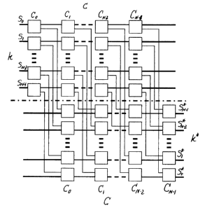
operation. Figure 4 illustrates the mathematic definition of the modified
optical cross-
connection for the NxN matrix optical switch based on the present invention.
As
mentioned above with Fig. 1 (a), the communication for an NxN matrix optical
switch is
operated between N input ports So , S, , through SN_, , and N the output ports
So , S; ,
through SN_, . As shown in Fig. 4, the columns of the switching units are
labeled Co , C, ,
through CN_, . For the communication between the input port k ( k = 0,1,..., N
-1 ) and
the output port k' ( k' = 0,1,..., N -1 ), only the column is needed to be
addressed for
connecting the output end of the switching unit at this column in the input
matrix and the
input end of the switching unit at this column in the output matrix as defined
by
C=(N-1)-(k+k'), for (k+k' ~N) (1)
C=(2N-1)-(k+k'), for (k+k' >-N) (2)
CA 02386352 2002-05-28
As mentioned above, each node indicates a switching unit and needs a 2x2 or
1x2 switch
to perform its options of links. As well known, in the low-index-contrast
waveguides,
typically there are two kinds of 2x2 optical waveguide switches: the MZI type
and the
DOS. The former has two main advantages: lower power consumption and lower
access
loss, and a main disadvantage: wavelength sensitivity. The latter has a main
advantage:
wavelength insensitivity and two main disadvantages: higher power consumption
and
higher access loss. The power consumption, the insertion loss and the
wavelength
sensitivity are three most important issues of an optical matrix switch based
on an feature
accumulation of all the switching units and the optical paths that optical
signals pass
through. Thus, the MZI type optical switch is preferred to use as a switching
unit because
it can directly meet two issues of the optical matrix switches with its two
main
advantages and its disadvantage: wavelength sensitivity can be solved by
another way in
this invention. If the wavelength sensitive switching units such as MZI type
optical
switches are used as the switching units of the NxN optical waveguide matrix
switch, at
the different columns, the switching units are designed for different central
wavelengths
to uniformly cover the whole wavelength range. So, the wavelength
sensitivities among
all the switching stages can be compensated for one another. Finally the
performance of
NxN optical matrix switch based on this invention should be added the
wavelength
insensitivity. In addition, the matrix optical switches based on the present
invention do
not have to be limited in NxN type. The MxN optical matrix switches can also
be built
based on the present invention wherein M 1xN optical switches and the N Mxl
optical
switches are used.
The waveguide switch based on the MZI configuration contains two 3dB
directional
couplers connected by two waveguide arms. This kind of switches basically
exploits the
phase property of the light. The input light is split and sent to two separate
waveguide
arms by the first 3dB directional coupler, then combined and split one last
time by the
second 3dB directional coupler. One or two of the waveguide arms are modulated
to
produce a dif,~erence of optical path length between these two waveguide arms.
The
modulating means can be either the TO or the EO. If these two optical paths
are the same
length, light chooses one exit, if they are different it chooses the other. As
a 2x2 switch,
for one input optical signal, the isolation between two output ports is of
importance. The
isolation is strongly dependent of the coupling ratio of the two 3dB
directional couplers.
Namely, the closer to 50% the coupling ratio of the 3d8 directional coupler
is, the higher
the isolation of the 2x2 switch is, and further more the higher the ON/OFF
extinction
ratio of each output port is. In theory, if the coupling ratio of the 3dB
coupler is exactly
50% (i.e., -3dB), the isolation between two output ports should be infinity.
In fact, no
perfect 3dB directional coupler exists because the errors in both design and
fabrication,
especially in fabrication, are not avoidable. So, a real isolation of around
20 dB is not
easy for any 2x2 waveguide switch having an MZI configuration to be achieved.
In the
real fiber-optic communications, not only is the isolation of more than 20 dB
popularly
required for the protection switching systems, but also the isolation of more
than 30 dB,
even more than 40 dB is always and strictly required for some more important
DWDM
networks such as typical optical add/drop multiplexing systems. Fortunately,
in the NxN
optical matrix switches based on the present invention, all the optical
signals pass through
CA 02386352 2002-05-28
the same number of MZI units (N+1), so each optical signal has N+1 MZI
operations and
only two of these N+1 MZI units are activated. So, not only the uniformity of
optical
performance among all the ports can be achieved a high level, but also the
isolation is
easy to meet because it is based on the accumulated effect of N+1 MZI
operations. In
accordance with the operating principle of the NxN optical switches based on
the present
invention, the switching unit must operate the bar-state output at the OFF-
state and the
cross-state output at the ON-state, so only the inverse type of 2x2 MZI
optical switch is
suggested to use. Of course, the normal type MZI units, which operate the
cross-state
output at the OFF-state and the bar-state output at the ON-state, can also be
used because
the design for a normal type 2x2 MZI optical waveguide switch is easier than
the inverse
type 2x2 MZI optical waveguide switch, but the permutation among all the
switching
units and distribution of waveguide paths are relatively difficult compared to
the use of
the inverse type of 2x2 MZI optical switches.
Figure 5 shows the inverse type of 2x2 MZI optical switch where Figure 5(a) is
the
schematic of the electrode (heater) for the TO modulation and Figure 5(b) is
of the
electrodes for the EO modulation. The inverse MZI unit is composed of two 3dB
directional couplers 48a and 486 connected by two waveguide arms. As shown in
Fig. 5,
between two 3dB directional couplers 48a and 48b, two waveguide arms have
phase
difference of ~ or an odd integer of ~t. So, this type of MZI is called as
inverse MZI
configuration. For the TO modulation, as shown in Fig. 5(a), one heater 50 is
deposited
on one of two arms and used to modulate the optical path of MZI unit with a TO
effect.
For the EO modulation, as shown in Fig. 5(b), two electrodes 50a and 50b are
deposited
on the two sides of one waveguide arm and used to modulate the optical path of
MZI unit
with an EO effect whereof waveguides are generally formed by the diffused
LiNb03 or
EO polymers. Two input pons are labeled as 52a and 52b, and two output ports
as 54a
and 54b. If an optical signal 56a is launched into the input port 52a, it is
split into two
parts at 50% coupling ratio by the first 3dB directional coupler 48a and then
these two
parts are combined into one optical signal again by the second 3dB directional
coupler
48b. For either the TO modulation as shown in Fig. 5(a), if the heater (or
electrode) 50 is
not activated (at the OFF-state) or the EO modulation as shown in Fig. 5(b),
if the
electrodes 50a and SOb are not activated (at the OFF-state), there has been an
optical
phase difference of ~ between two waveguide arms, so the combined optical
signal is
sent to output port 54a. This coupling process is exactly the inverse to one
100%
directional coupler that the normal MZI configuration should have, so it is
called inverse
MZI configuration. If the heater 50 is activated by electrical power for the
TO
modulation or the electrodes 50a and 50b are activated by electric field to
produce an
extra optical phase change of ~t (at the ON-state) so that the optical phase
difference
between two waveguide arms becomes 0 or an even integer of ~t, this combined
optical
signal 56a is sent to the output port S4b by the second 3dB directional
coupler 48b. In the
same manner, if an optical signal 56b is launched into input port 52b, it will
come out at
the output port 54b at the OFF-state and come out at the output port 54a at
the ON-state.
What is described above is mainly based on the low-index-contrast waveguides
(Typically D = 0.3% - 2.0% ) no matter the TO or the EO modulation is used in
the
waveguide switches. In fact, the other type of waveguides, high-index-contrast
CA 02386352 2002-05-28
waveguides (Typically core: cladding index is 1.5:1 up to 3.5:1) also receives
much more
attention in industry because the high-index-contrast waveguides can really
give some
paramount advantages over the law-index-contrast waveguides. Typically, the
high-
index-contrast waveguides supporting tightly confined modes act as optical
wires, so they
can be bent, twisted, and split without any loss of light. But, the high-index-
contrast
waveguides really have inherent drawbacks compared to the low-index-contrast
waveguides. Typically, the crossings of the high-index-contrast waveguides can
result in
considerable scattering and cross talk at the intersecting junctions, but the
low-index-
contrast waveguides can pass through one another with little interference.
More
importantly the high-index-contrast waveguides can form new functional
components
such as microring resonators as building blocks for the very large-scale
integrated (VLSI)
photonics and it is possible for these new functional components to become
active and
non-wavelength-selective such as 2x2 or 1x2 optical switches. Once this type
of optical
switching units based on the high-index-contrast waveguides are available, the
NxN
optical matrix switches based on the present invention can be implemented with
a two-
layer regime that uses the high-index-contrast waveguides to form the 2x2 or
1x2
switching units at the top layer and the low-index-contrast waveguides to
carry optical
signals or beams. Then the optical matrix switches based on the present
invention will
perform a significant potential in applications with a radically different
concept because
the high-index-contrast and the low-index-contrast waveguides are independent
and both
of them are working at their own optimized points. In addition, the NxN
optical matrix
switches based on the present invention can also be implemented directly with
fiber
couplers where the modulation can be based on the TO effect, a magnetic-optic
(MO)
effect, a pressure, or others. To date, the commercially mature fiber couplers
mainly
include the polished fiber coupler and the fused fiber coupler. The former has
the access
loss of light for each coupler is about O.OOSdB, which is much lower than what
is for the
best cases in the waveguide couplers. The later has the access loss of light
for each
coupler is about O.IdB. Although the access loss is relatively high compared
to the
polished one, it needs a much easier fabrication technique.