Note: Descriptions are shown in the official language in which they were submitted.
CA 02386679 2002-04-04
WO 01/27670 PCT/GB00/03935
1
METHOD OF FABRICATING AN INTEGRATED
OPTICAL COMPONENT
TECHNICAL FIELD
This invention relates to a method of fabricating an integrated optical
component on a silicon-on-insulator (S01) chip comprising a layer of silicon
separated from a substrate by an insulating layer, the component having a
first set of features at a first level in the silicon layer and a second set
of
features at a second level in the silicon layer. The invention also relates to
an
optical component obtainable by the method.
BACKGROUND ART
Integrated optical components may be fabricated in the silicon layer of an SOI
chip. The silicon layer is typically up to 5 microns thick (but, in some
cases,
may be up to 10 microns thick) and features are defined therein by
photolithographic techniques. Such optical components need to be fabricated
with a high degree of accuracy to enable them to function correctly and known
fabrication methods produce satisfactory yields for components formed on
such chips.
In some cases, however, e.g. where a low loss optical connection is required
between an integrated optical component and an optical fibre, there is a need
to increase the thickness of the silicon layer, e.g. up to 13 microns or
higher.
If the SOI chip is initially fabricated with a silicon-layer of lower
thickness, the
thickness of the layer can be increased e.g. by epitaxial growth. Problems
are, however, encountered in fabricating optical components in such thick
silicon layers with sufficient accuracy, particularly when two stages of
photolithography are required to form features at two different levels in the
silicon layer. There are two principal reasons for the problem. Firstly, the
thickness of the silicon layer of an SOI chip is not uniform and the thicker
the
layer, the greater the variations. Secondly, the accuracy with which a
feature,
particularly a depth dimension, can be etched, decreases with the thickness of
the silicon layer, i.e. the deeper the etch the greater the variation in its
SUBSTITUTE SHEET (RULE 26)
CA 02386679 2002-04-04
WO 01/27670 PCT/GB00/03935
2
dimensions. These two sources of inaccuracy tend to be accumulative. The
problems become worse as the depth of the silicon layer and hence the depth
of the features to be fabricated therein increase. This results in a gradual
reduction in yield as thicker silicon layers are used and it has been found
that
the yield may fall to an unacceptably low level for components fabricated in a
silicon layer having a thickness of 10 microns or more.
The invention aims to provide an improved method of fabricating integrated
optical components which increases the yield in such circumstances.
DISCLOSURE OF INVENTION
According to a first aspect of the invention there is provided a method of
fabricating an integrated optical component on a silicon-on-insulator chip
comprising a silicon layer separated from a substrate by an insulating layer,
the component having a first set of features at a first level in the silicon
layer
adjacent the insulating layer and a second set of features at a second level
in
the silicon layer further from the insulating layer, the method comprising the
steps of:
selecting a silicon-on-insulator chip having a silicon layer of sufficient
thickness for the first set of features;
fabricating the first set of features in the silicon layer so as to form said
first set of features at a first level in the silicon layer;
increasing the thickness of the silicon layer in selected areas so as to
form a second level of the silicon layer over at least part of the first
level; and
fabricating the second set of features at the second level in the silicon
layer
SUBSTITUTE SHEET (RULE 26)
CA 02386679 2002-04-04
WO 01/27670 PCT/GB00/03935
3
Accordingly to a further aspect of the invention there is provided an
integrated
optical component obtainable by such a method.
According to another aspect of the invention there is provided an integrated
optical component on a silicon-on-insulator chip comprising a silicon layer
separated from a substrate by an insulating layer comprising a first set of
features at a first level in the silicon layer adjacent the insulating layer
and a
second set of features at a second level in the silicon layer further from the
insulating layer, wherein the thickness of the silicon layer is 10 microns or
more and the depth dimensions of the first set of features are formed to an
accuracy of ~ 1.5%.
According to yet another aspect of the invention there is provided an
integrated optical component on a silicon-on-insulator chip comprising a
silicon layer separated from a substrate by an insulating layer, the component
comprising a rib waveguide formed in the silicon layer so as to overhang an
inclined end face of a V-groove formed in the chip, the end of the waveguide
comprising a tapered structure in the form of a triangular shaped portion on
top of the rib waveguide and comprising a widened portion in the form of a T-
bar at the wide end of said tapered structure.
Preferred and optional features will be apparent from the following
descriptions and from the subsidiary claims of the specification.
BRIEF DESCRIPTION OF DRAWINGS
The invention will now be further described, merely by way of example, with
reference to the accompanying drawings, in which:
Figures 1 A, 1 B and 1 C illustrate sources in inaccuracy of the fabrication
of
integrated optical circuits.
SUBSTITUTE SHEET (RULE 26)
CA 02386679 2002-04-04
WO 01/27670 PCT/GB00103935
4
Figure 2A is a plan view of an integrated optical waveguide having wedge-
shaped tapers at each end, and Figures 2B and 2C are cross-sectional views
across the waveguide at lines B-B and C-C of Figure 2A;
Figure 3 is a perspective view of one end of a waveguide such as that shown
in Figures 2A;
Figures 4A, 4B 4C and 4D illustrate a method according to the present
invention for the fabrication of features of a component such as those shown
in Figure 2C;
Figure 5 corresponds to Figure 4C and illustrates the crystalline structure of
the silicon layer as its thickness is increased;
Figure 6 is a perspective view of one end of another waveguide; and
Figure 7 is a perspective view of one end of a still further waveguide.
BEST MODE OF CARRYING OUT THE INVENTION
Figures 1 A, 1 B and 1 C are schematic diagrams of a cross-section through a
silicon-on-insulator (S01) chip comprising a silicon layer 1 separated from a
substrate 2, typically also of silicon, by an insulating layer 3, typically of
silicon dioxide.
Figure 1A shows variations (shown exaggerated) in the thickness of the
silicon layer which is nominally 5 microns thick. Such variations may be in
the
order of ~ 5%, i.e. around ~ 0.25 microns for a 5 mm thick silicon layer.
Figure 1 B shows variations (again, shown exaggerated) in the thickness of a
silicon layer which is nominally 10 microns in thickness. Again, the thickness
of the layer is subject to variations of ~ 5%. i.e. around ~ 0.5 microns for a
10
micron thick silicon layer.
SUBSTITUTE SHEET (RULE 26)
CA 02386679 2002-04-04
WO 01/27670 PCT/GB00/03935
Figure 1 C shows a recess etched in the silicon layer. The depth of the recess
can only be controlled to an accuracy of ~5%, particularly for etch depths
greater than 5 microns, resulting in variations of the etch depth of +0.25
microns or more.
These sources of error are accumulative so the overall variation in the etch
depth, and thus the thickness of the silicon layer remaining at the base of
the
recess in Figure 1 C, can vary by up to ~ 0.75microns. Such a level of
variation may be unacceptable in mass produced components as a high
proportion of components have to be rejected as they are not formed within
the required tolerance.
Figure 2A is a plan view of a rib waveguide 5 formed in the silicon layer of
an
SOI chip. The rib of such a waveguide typically has a height of around 1.5
microns (measured from the surface of the adjacent areas of silicon).
Tapered structures 6 are provided at the ends of the waveguide between the
rib waveguide 5 and the end faces 6A which are to be coupled with optical
fibres (not shown) so the end faces 6A have a size more compatible with the
size of the core of the optical fibre. Tapered structures 6 comprise a
triangular-shaped upper portion 6B on top of the rib waveguide 5. Further
details of such a tapered structure are given in W098/35250 the disclosure of
which is incorporated herein. The triangular portion 6B, as described in
W098/35250, typically has a thickness of about 5 microns so the overall
thickness of the waveguide from the insulating layer 3 to the upper surface of
the triangular portion 6B, is around 10 microns. However, as indicated above,
a need arises in some cases for this thickness to be increased to 13 microns
or more in which case the thickness of the triangular portion needs to be 8
microns or more.
Figure 2B is a cross-section along line B-B of Figure 2A and shows a section
through a portion of the rib waveguide 5. Figure 2C is a cross-section along
line C-C of Figure 2A and shows a section through a triangular portion 6B part
way along its length.
SUBSTITiJTE SHEET (RULE 26)
CA 02386679 2002-04-04
WO 01/27670 PCT/GB00/03935
6
Figure 3 shows a perspective view of a tapered structure 6 at one end of a
waveguide 5 as shown in Figure 2A. The end face 6A of the waveguide is
also provided with a widened portion 6C, known as a "T-bar", as disclosed in
GB2334789A. The end of the waveguide 5 and the tapered structure 6 are
also formed on a portion 1 A of the silicon layer which overhangs the inclined
end face 7A of a V-groove 7 for receiving an optical fibre (not shown). The
use of such an overhang for coupling an integrated waveguide to an optical
fibre is described in W097/42534.
Figures 4A, 4B 4C and 4D illustrate steps involved in fabricating an
integrated
optical component such as that described in relation to Figures 2 and 3. It
will
be appreciated that the waveguide structure shown in these figures comprises
a first set of features at a first level in the silicon layer 1, i.e. the rib
5 and
recess 8 on either side thereof, these features being formed in a level of the
silicon layer 1 up to 5 microns from the insulating layer 3, and a second set
of
features at a second level in the silicon layer 1, i.e. the triangular portion
6B a
level of the silicon layer between 5 and 13 microns from the insulating laser.
To avoid the problems associated with fabricating such features in a silicon
layer having a thickness greater than 10 microns, an SOI chip having a silicon
layer of sufficient thickness to form the first set of features, i.e. the rib
waveguide 5, is initially selected. The silicon layer preferably has a
thickness
of 10 microns or less and, most preferably, of 5 microns. A rib waveguide is
fabricated in this silicon layer by etching the recesses 9 on either side
thereof
by known lithographic processes resulting in a structure as shown in Figure
4A. This figure also shows an oxide layer 10 covering the rib waveguide 5,
the recesses 9 and the adjacent silicon layer 1. Such a structure can be
formed with great accuracy as it is a relatively planar structure, as
variations in
the thickness of the silicon layer 1 are small, as the thickness of the layer
1 is
small (e.g. around 5 microns), and because the recesses 9 to be etched are
relatively shallow, e.g. around 1.5 microns. Recesses of such depth can
typically be formed to an accuracy of ~1.5%.
SUBSTITL7TE SHEET (RULE 26)
CA 02386679 2002-04-04
WO 01/27670 PCT/GB00/03935
7
The oxide layer on the upper surface of the rib waveguide 5 in the region
where the second set of features, i.e. the triangular portion 6B, are to be
formed is then removed as shown in Figure 4B, e.g. by etching.
The thickness of the silicon layer over the exposed areas of the initial
silicon
layer is then increased, e.g. by epitaxial growth, to produce the structure
shown in Figure 4C. This growth may be selective or non-selective, or a
combination. Selective growth meaning that single crystal Si grows on
exposed Si surfaces only, whilst no growth takes place on exposed oxide
layers. In non-selective growth, single crystal Si grows on exposed Si
surfaces and polycrystalline Si grows on exposed oxide surfaces. For
selective growth, HCI can be added to the gas mixture.
As shown in Figure 4C, the structure formed has a relatively flat top surface
suitable for receiving photolithographic masks. The thickness of the silicon
layer is preferably increased by at least 5 microns and most preferably by at
least 8 microns. In some cases, it may be desirable to grow the layer thicker
than necessary and then polish the top of the layer by chemical/mechanical
polishing (CMP) to achieve a flat surface.
A high resolution photo-resist 12 is then deposited over the areas of the
silicon layer 11 which are to remain (as shown in Figure 4C) and the
remaining areas of the layer 11 are etched away to leave the structure shown
in Figure 4D. The second set of features, i.e. the shape of the triangular
portion 6B, are thus formed in the second level of silicon provided on top of
the first level of silicon and formation of this second set of features does
not
disturb the first set of features, i.e. the rib waveguide 56 etc., formed in
the
first level of the silicon layer 1.
In an alternative arrangement, the shape of the triangular portion 6B may be
defined by a triangular trench etched around the portion 6B. The silicon layer
SUBSTITUTE SHEET (RULE 26)
CA 02386679 2002-04-04
WO 01/27670 PCT/GB00/03935
8
formed over the oxide layer over the remainder of the chip does not then need
to be removed. This is illustrated more fully in figure 7.
The problems discussed above are thus avoided by fabricating the silicon
layer in two stages and by fabricating features in the first level of the
silicon
layer before the second level of the silicon layer is formed. This two-stage
method thus enables components having a relatively large thickness, e.g. of
microns or more, measured from the insulating layer 3, to be fabricated
with greater accuracy and greater consistency, so increasing the yield in the
mass production of such components.
In an alternative form of the method described above, the silicon layer 11 may
be formed by depositing amorphous polycrystalline silicon over the structure
shown in Figure 4B. The unwanted areas of the layer 11 can then be etched
away in the manner described above. The resulting structure may then need
to be heated to around 1100°C to re-crystallize the silicon in the
remaining
areas of the layer 11. The re-crystallized area tends to grow from the
boundary with the lower silicon level so helping to reduce defects in the
boundary between the two levels.
When silicon is deposited by selective epitaxial growth, as described above,
it
forms a single crystal over the exposed area of the silicon layer 1 on the top
surface of the rib waveguide 5 without the need for heat treatment.
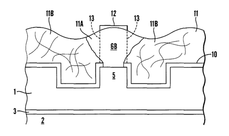
Figure 5 shows the crystalline structure of the silicon grown or deposited to
increase the thickness of the silicon layer. A single crystal area 11A forms
over the exposed area of the lower level of silicon, either by epitaxial
growth
therefrom or when the amorphous silicon is heated. The remainder of the
silicon deposited or grown over the oxide layer tends to be polycrystalline as
shown in the areas 11 B but his is etched away as described above in relation
to Figures 4C and 4D. The dashed lines 13 in Figure 5 indicate the
boundaries between the silicon to be etched away and that which remains to
form the triangular portion 6B.
SUBSTITUTE SHEET (RULE 26)
CA 02386679 2002-04-04
WO 01/27670 PCT/GB00/03935
9
Figure 6 shows an end of a waveguide according to the present invention. In
a first silicon layer 18, a first waveguide element 20 is defined by trenches
22,
24 on either side. It extends towards the edge 26 of the wafer but terminates
before the end at 28 where the trenches end. The trenches narrow slightly
prior to ending and thus the width of the waveguide increases slightly.
In a second layer of silicon 30, separated where necessary from the first by
an
intervening oxide layer 31, a short second waveguide element 32 extends
from the widening section of the first waveguide element 20 to the edge 26 of
the wafer. The tip of the second waveguide element 32 over the widening
section of the first ends with progressively narrowing width down to a taper.
Light propagating in the first waveguide element 20 is coupled into the second
waveguide element 32 by the widening of the first element 20 and the
development of the second element 32 from its taper point. The light is thus
brought up into the second waveguide element 32 which can be of a larger
dimension more suited to coupling to devices external to the wafer such as
optical fibres. The process can also operate in reverse to couple light into a
waveguide on the wafer.
Figure 7 shows a variant on the arrangement of Figure 6. A generally similar
structure is formed in the first silicon layer 18'. However, a lesser amount
of
silicon is removed from the second layer 30', the second waveguide element
32' being defined instead by a V-plan trench 34 around its perimeter.
A similar two-stage process may be used to fabricate other integrated
components on a silicon-on-insulator chip, particularly components having a
first set of features, e.g. a rib waveguide, at a first level in the silicon
layer, e.g.
up to 5 microns from the insulating layer, and a second set of features at a
second level in the silicon layer where the second layer has a thickness of 5
microns or more or even 8 microns or more.
SUBSTITUTE SHEET (RULE 26)
CA 02386679 2002-04-04
WO 01/27670 PCT/GB00/03935
The process may also be extended to three or more stages, e.g. in which
three or more levels of silicon are formed at different stages and features
are
formed in each layer before the subsequent layer is formed. W098/35250
describes a three level tapered structure which could be formed by such a
three-stage process.
SUBSTITUTE SHEET (RULE 26)