Note: Descriptions are shown in the official language in which they were submitted.
CA 02387154 2006-07-28
RCA 87,609B
1
TRANSPORT PACKET FILTER FOR PACKET VIDEO SYSTEM
This application is a division of Canadian Serial No. 2,188,127 filed
March 15, 1995.
This invention relates to apparatus for processing packets of program
component data from a packet video signal and more particularly to circuitry
for
detecting packet payloads to which a subscriber has conditional access for
entitlement information.
BACKGROUND OF THE INVENTION
It is known from, for example, U.S. Patent No. 5,168,356 and U.S.
Patent No. 5,289,276, that it is advantageous to transmit compressed video
signal
in packets, with respective packets affording a measure of error
protection/correction. The systems in the foregoing patents transmit and
process
a single television program, albeit with a plurality of program components,
from
respective transmission channels. These systems utilize inverse transport
processors to extract the video signal component of respective programs for
further processing to condition the video component for reproduction.
It is known, from for example, THE SATELLITE BOOK, A
COMPLETE GUIDE TO SATELLITE TV THEORY AND PRACTICE, Swift
Television Publications, 17 Pittsfield, Cricklade, Wilts, England, that
transmitted
television signal reception can be limited to particular subscribers by
scrambling
the signal. The limitations may be altered at the will of the broadcaster by
periodically transmitting different entitlement data. The entitlement data is
processed by smart cards located in respective receivers to generate deception
or
descrambling keys, for use by decryption or descrambling devices in only those
receivers entitled to reproduce the associated program material. In a packet
video
system of the aforementioned type, entitlement data may be included in
specific
packets which are recognizable as containing such data for easy access by
smart
card circuitry.
A large area broadcast system, such as a direct broadcast
satellite system targeted for North America, will have very large
numbers of subscribers. This number will be so large
CA 02387154 2002-06-20
2
as to preclude changing the entitlement data of specific receivers
on very short notice. Consider, for example, that a broadcaster is
required to black out the area local to a sports stadium in the
event that tickets for the sporting event are not sold out. This
information may not be available until immediately before the
event. The broadcaster of course will want to wait until the last
possible minute before making the decision to black out the local
region. The present invention provides a method and apparatus
whereby entitlement data is layered to provide denial of
entitlements to receive program material on short notice.
The present itivention is a system/method for layered
entitlement data transmission/reception. A receiver embodiment
includes a packet transport processor for selecting packets having
payloads containing a conditional access payload header and a
reniaining payload of entitlement data. Respective payload
headers include groups of bytes which are coded in a manner to
allow or disallow the respective receiver from processing the
entitlement data. A conditional access filter preprogrammed with
a subscriber specific conditional access codeword examines
respective byte groupings of the conditional access header for a
niatch with the subscriber specific conditional access codeword.
Only if a match occurs is the processor permitted to process the
ent-itlement data.
BRIEF DESCRIPTION OF THE DRAWINGS
The invention will be described with reference to the
drawings, wherein:
FIGURE I is a pictorial representation of a time
division multiplexed packet television signal;
FIGURE 2 is a pictorial representation of respective
signal packets;
FIGURE 3 is a block diagram of a receiver for selecting
and processing packets of multiplexed component signals
embodying the present invention;
CA 02387154 2002-06-20
3
FIGURE 4 is a block diagram of a conditional access
filter/start code detector;
FIGURE 5 is a flow chart of the conditional access filter
operation;
FIGURE 6 is a block diagram of an alternative
conditional access filter;
FIGURE 7 is a block diagram of exemplary memory
] 0 management circuitry which may be implemented for element 17
of FIGURE 3;
FIGURE 8 is a pictorial representation showing
memory address formation for service channel data.
FIGURE 9 is a flow chart of operation of the memory
1 5 address control.
FIGURE 1 shows a packet signal stream consisting of a
string of boxes which represent signal packets that contain
components of a plurality of different television or interactive
television programs. These program components are assunied to
20 be formed of conipressed data and as sucti the quantity of video
data for respective images is variable. The packets are of fixed
length. Packets with letters having like subscripts represent
components of a single program. For example, Vi, Ai, Di represent
video, audio and data packets and packets designated Vi, A I, D 1,
25 represent video, audio and data cornponents for program 1, and
V3, A31, A32, D3, represent video, audio l, audio 2 and data
components of program 3. The data packets Di may contain e.g.
control data to initiate certain action within a receiver, or they
may include executable code forming an application to be
30 executed by e.g., a microprocessor located within or associated
with a receiver.
In the upper line of the string of packets the
respective components of a particular program are shown grouped
together. However there is no necessity of packets from the same
35 prograrn being grouped as is indicated by the entire string of
CA 02387154 2002-06-20
4
packets. Nor is there any particular order for the sequence of
occurrence of respective components.
The respective packets are arranged to include a
prefix and a payload as shown in FIGURE 2. The prefix of this
example includes two 8-bit bytes comprising five fields, four (P,
BB, CF, CS) of which are 1-bit fields, and one (SCID) of which is a
12-bit field. The SCID field is the signal component identifier.
The field CF contains a flag to indicate whether the payload of the
packet is scrambled, and the field CS contains a flag which
indicates which of two alternative unscrambling keys is to be
utilized to unscramble scrambled packets. The- prefix of every
packet is packet aligned, thus the location of the respective fields
are easily identifiable.
Within every payload is a header which contains a
continuity count, CC, modulo 16, and a TOGGLE flag bit which are
program component specific. The continuity count is simply a
successive numbering of sequential packets of the same program
component. The TOGGLE flag.bit is a one bit signal which changes
logic level or toggles on the occurrence of a picture layer start
code in an MPEG compressed video component.
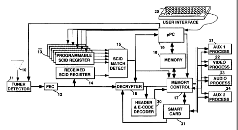
FIGURE 3 illustrates in block form, a portion of a
digital television signal receiver including elements of an inverse
transport processor. Signal is detected by an antenna 10 and
applied to a tuner detector, 11, which extracts a particular
frequency band of received signals, and provides baseband
compressed signal in a binary format. The frequency band is
selected by the user through a microprocessor 19 by conventional
methods. Nominally broadcast digital signals will Ilave been error
encoded using, for example, Reed-Solomon forward error
correcting (FEC) coding. The baseband signals will thus be applied
to a FEC decoder, 12. The FEC decoder 12 synchronizes the
received video and provides an error corrected stream of signal
packets of the type illustrated in FIGURE 1. The FEC 12 may
provide packets at regular intervals, or on demand, by for
CA 02387154 2002-06-20
example, memory controller 17. In either case a packet framing
or synchronizing signal is provided by the FEC circuit, which
5 indicates the times that respective packet information is
transferred from the FEC 12.
The detected frequency band may contain a plurality
of time division multiplexed programs in packet form. To be
useful, only packets from a single program should be passed to
the further circuit elements. In this example it is assumed that
the user has no knowledge of which packets to select. This
information is contained in a program guide, which in itself is a
program consisting of data which interrelates program signal
components through SCID's, and may include information relating
to, for example, subscriber entitlements. The program guide is a
listing for each program, of the SCID's for the audio, video, data
etc. components of respective programs. The program guide
(packets D4 in FIGURE 1) is assigned a fixed SCID. When power is
applied to the receiver, the microprocessor 19 is programmed to
load the SCID associated with the program guide into one of a
bank of similar programmable SCID registers 13. The SCID fields
of the prefix portion of respective detected packets of signal from
the FEC 12 are successively loaded in a further SCID register 14.
The programmable registers and the received SCID register are
coupled to respective input ports of a comparator circuit 15, and
the received SCID is compared with the program guide SCID. If
the SCID for a packet matches the program guide SCID, the
comparator 15 conditions a memory controller 17 to route that
packet to a predetermined location in the memory 18 for use by
the microprocessor. If the received SCID does not match the
program guide SCID, the corresponding packet is simply dumped.
The microprocessor waits for a programming
command from the user via an interface 20, which is shown as a
computer keyboard, but which may be a conventional remote
control, or receiver front panel switches. The user may request to
view a program provided on channel 4 (in the vernacular of
CA 02387154 2002-06-20
6
analog TV systems). The microprocessor 19 is programmed to
scan the program guide list that was loaded in the memory 18 for
the respective SCID's of the channel 4 program components, and to
load these SCID's in respective other ones of the programmable
registers of the bank of registers 13 which are associated with
corresponding component signal processing paths.
Received packets of audio, video or data program
components, for a desired program, must ultimately be routed to
the respective audio 23, video 22, or auxiliary data 21, (24) signal
processors respectively. The data is received at a relatively
constant rate, but the signal processors nominally require input
data in bursts (according to the respective types of decompression
for example). The exeniplary system of FIGURE 3, first routes ttie
respective packets to predetermined memory locations in the
common niemory 18. Ttiereafter the respective processors 21-24
request ttie component packets from the memory 18. Routing the
components through the common memory provides a measure of
desired signal data rate buffering or throttling.
The audio, video and data packets are loaded into
respective predeterrnined memory locations to enable the signal
processors convenient buffered- access to the component data. In
order that the payloads of respective component packets are
loaded in the appropriate memory areas, the respective SCID
comparators are associated with those memory areas. This
association may be hardwired in the memory controller 17, or the
association may be programmable. If the former, specific ones of
the programmable registers 13 will always be assigned the audio,
video and data SCID's respectively. If the latter, the audio, video
and data SCID's may be loaded in any of the programmable
registers 13, and the appropriate association will be programmed
in the memory controller 17 when the respective SCID's are
loaded in the programmable registers.
In the steady state, after the program SCID's have
been stored in the programmable registers 13, the SCID's of
CA 02387154 2002-06-20
7
received signal packets are compared with all of the SCID's in the
programmable SCID registers. If a niatch is made with either a
stored audio, video or data SCID, the corresponding packet
payload will be stored in the audio, video or data memory area or
block respectively.
The respective signal packets are coupled from the FEC
12 to the memory controller 17 via a signal decryptor 16. Only
the signal payloads are scrambled and the packet headers are
passed by the decryptor unaltered. Whether or not a packet is to
be descrambled is determined by the CF flag in the packet prefix,
and how it is to be descrambled (one of two alternative
descrambling keys) is determined by the CS flag. If no SCID
1 5 match is had for a respective packet, the decryptor may simply be
disabled from passing any data.
'I'he decryptor is programmed with decryption keys
provided by the smart card apparatus 31. The smart card is
responsive to entitlenient inforniation contained in particular
packets of the program guide . to generate appropriate decryption
keys. "I'he systern of the present example incorporates two levels
of encryption or program access, entitlement control niessages,
ECM's, and entitlement management messages, EMM's. Program
entitlement control and nianagetnent information is regularly
transmitted in packets identifiable with specific SCID's included in
the packet stream comprising the program guide. The ECM
information contained in these packets is used by the smart card
to generate the decryption keys used by the decryptor. The EMM
information included in these packets is used by the subscriber
specific smart card to determine progratn material to which the
subscriber is entitled. EMM entitlement information within these
packets may be made geographically specific, or group specific or
subscriber specific. For example, the present system will include
a nlodem (not shown) for communicating billing information from
3 5 the smart card to the program provider, e.g., the satellite
broadcaster. The smart card may be programmed with, for
CA 02387154 2002-06-20
8
example, the area code and telephone exchange of the receiver
location. The EMM may include data, which when processed by
the smart card, will entitle or deny reception of particular
programs in particular area codes.
The program provider may want the ability to entitle
certain subscribers with very short lead time, as for example for
pay-per-view programs. The identification of particular
subscribers may not be available until shortly before airing of the
particular program. With such short lead time it may not be
possible to program EMM's on a subscriber basis. A further layer
of coding may be instantly impressed on the entitlement
information by including a conditional access code to
1 5 permit/prohibit reception of the EMM and ECM data within
respective packets, and thereby allow substantially instant
permission/proliibition to certain programs.
Packet payloads containing the EMM and ECM
entitlement data include a payload header of 128 bits arranged in
specially coded 4 groups of 32 bits. Eacti of the groups is coded
with a conditional access code and each conditional access code
may be coded differently. Each subscriber is assigned a specific
conditional access code. A matched filter or E-code decoder 30, is
arranged to detect a subscriber specific bit pattern witliin the 128
bit - header. If a match is detected the decoder comrnunicates with
the memory controller 17 and the smart card 31 to make the
remainder of the entitlement payload available to the smart card
(via ttie memory 18). If a match is not detected, the payload is
not accepted by the specific receiver. The conditional access codes
may be periodically changed if the matched filter 30 is made
programmable. These codes niay be periodically provided by the
smart card. For more specific details on smart card operation as
related to viewer entitlements the reader is invited to review
Section 25 of THE SATELLITE BOOK, A COMPLETE GUIDE TO
SATELLITE TV THEORY AND PRACTICE,.
CA 02387154 2002-06-20
9
The matched filter or E-code decoder is arranged to
perform a second function, which is to detect particular MPEG
video headers. These headers are 32-bit start codes, (which is the
reason the headers of entitlement payloads are coded in 32-bit
groups). If video data is lost, an MPEG video decoder can only
restart decompressing video data at particular data entry points.
These entry points coincide with MPEG start codes. The decoder
may be arranged to communicate with the memory controller 17
to inhibit the flow of video data to memory after video packet
losses, and to resume writing video payloads to memory only
after the next MPEG start code is detected by the decoder 30.
FIGURE 4 illustrates exemplary apparatus for detecting
1 5 packets which include conditional access information or MPEG
start codes (decoder 30 of FIGURE 3). Whether the decoder 30 is
conditioned to detect entitlement payloads or MPEG start codes is
a function of the SCID currently being received. In FIGURE 4, it is
assumed that data provided from the decryptor 16 is in 8-bit
bytes and packet aligned. That is, the first byte of an entitlement
payload or the first byte of an MPEG start code is aligned precisely
with a particular byte position, e.g., the beginning of a packet
payload, such ttiat for detecting specific header or start
codewords, their position in the bit/byte stream is precisely
known. Data from the decryptor 16 is applied to an 8-bit register
250, which lias an 8-bit parallel output port coupled to respective
first input connections of a comparator 254 which may be
configured of, for example, a bank of eight two-input exclusive
NOR (XNOR) circuits having respective output connections coupled
3 0 to an AND gate and a latch. The latch may be a data latch
arranged to latch the results of the AND gate at each byte interval.
A 32-bit MPEG start code is stored as four bytes in an
8-bit register bank 265. Conditional access codes are stored as 8-
bit bytes in a bank of 16 8-bit registers 257. Loading of the
register banks 251 and 265 is controlled by the microprocessor 19
and/or by the smart card. The start code registers 265 are
CA 02387154 2002-06-20
coupled to a four to one multiplexer 266, and the conditional
access code registers are coupled to a sixteen to one multiplexer
5 257. Output ports of the multiplexers 257 and 266 are coupled to
a two to one multiplexer 249. Respective output connections of
the multiplexer 249 are coupled to respective corresponding
second input terminals of the comparator 254. (Note the input
and output connections of the multiplexers 249, 257 and 266 are
10 8-bit busses.) If the respective values exhibited at the respective
output connections of the register 250 are correspondingly the
same as the output values exhibited by the respective output
connections of the multiplexer 249, a true signal is generated by
the comparator 254 circuit for the corresponding data byte.
For start code detection, the multiplexer 266 is
scanned by the counter 258 to sequentially couple the four
different registers 265 to the comparator in synchronism with the
occurrence of the first four payload data bytes from the decryptor
16. Alternatively, for conditional access code detection, the
multiplexer 257 is scanned by. the counter 258 to sequentially
couple different ones of the registers 265 to the comparator
circuit 254.
The output of the comparator circuit is applied to an
accumulate and test circuit 255. "The circuit 255 determines if any
of -a predetermined number of byte matching conditions have
occurred, and if they have, it generates a write enable signal for
the entitlement data in the remaining portion of the particular
payload under examination. In the present system the
entitlement payload header contains 128 bits arranged in four 32-
3 0 bit conditional access codes. The conditional access filters 30 of
different subscribers will be arranged to look for different
combinations of bytes of the 128 bits. For example one subscriber
apparatus may be arranged to match the first four bytes of the
conditional access codes. Another subscriber apparatus may be
arranged to match the second four bytes of the conditional access
codes and so forth. In either of these exemplary situations the
CA 02387154 2002-06-20
11
circuitry 255 will determine if a match has occurred for the
appropriate four consecutive bytes.
The use of 16 registers in the bank for a subscriber
specific conditional access codes somewhat simplifies the circuit
structure. Since each subscriber has a four byte conditional access
code, the code may be loaded four times in the set of 16 registers.
At the transmitter, the broadcaster need not then be concerned
about the relative location, with respect to the four groups of four
bytes, of the conditional access codes being transmitted. An
alternative arrangement may incorporate only a single group of
four registers to hold the subscriber specific conditional access
code, and these registers may be repeatedly scanned, modulo four,
through ttie 128 bits of the entitlement payload header.
It is not practical to transmit each of the 232 possible
entitlement codes for every function, as this would undesirably
limit the systeni bandwidth for other services and would also
simply take too much time. This limitation may be somewhat
alleviated by arranging the conditional access code according to
some logical groupings, wherein the groupings are defined by
three bytes of respective four byte conditional access codes. In
this manner all subscribers in -a group may be addressed by
coiiditioning respective receivers of the group to ignore one byte
of -the four byte conditional access code. In this instance each four
byte access code will represent 256 subscribers. The filter
conditioning is effected by sending for example all zeroes in the
first four byte positions and arranging the conditional access filter
to detect this condition. If the condition is satisfied, the
conditional access filter is electrically restructured to detect a
match of only three bytes of respective groups of four bytes.
A third variant is provided to permit all subscribers
conditional access. This is effected by coding the entitlement
payload header with all zeroes (or all ones). The conditional
access filter is therefore arranged to also include an all zero
detector (elements 261-263).
CA 02387154 2002-06-20
12
The bits of respective arriving bytes of data are
coupled to respective terminals of the 8-bit OR gate 263. If any
one of the bits is a logic one the OR gate 263 generates a logic one
output. The output of the OR gate 263 is coupled to one input of a
two-input OR gate 262, which has an output and second input
coupled respectively to the data-input and Q-output terminals of a
D-type latch 261. The D-type latch is clocked by the timing circuit
259 synchronously with the arrival of incoming data bytes. If any
bit in any of the data bytes which occurs after the latch is reset is
a logic one, the latch 261 will exhibit a logic one at its Q-output
until the next reset pulse. The Q-output of latch 261 is coupled t.o
an inverter which exhibits a zero output level whenever the latch
1 5 exhibits a one output level. Thus, if after the 128 bits (16 bytes)
of the header have been passed through register 250, the output
of the inverter is high, then the 128 bits are zero valued. The
latch is reset prior to the reception of each new payload.
Responsive to detection of a high output level from the inverter
2 0 after passage of the entitlement payload header, the circuitry 255
will generate a data write enable signal.
FIGURE 5 is a flow chart of the operation of the
conditional access filter 30. The process is started by the
detection of the associated SCID. Once the appropriate SCID has
2 5 been detected the payload is applied (300) to the filter 30. A
comparison (302) is made of the first four bytes of the header
with the subscriber specific conditional access code. If a match
occurs, an entitlement data write enable is generated (310). If not
the first four bytes are examined 1306) for all zeroes. If all zeroes
3 0 are not detected, the second four bytes of the header are
compared (3081 with the subscriber specific conditional access
code. If they match (312), a write enable is generated f310]. I f
not the third set of four bytes is compared (314) with the
subscriber specific conditional access code. If they match (316), a
3 5 write enable is generated (310). If not, the fourth set of four
bytes is compared (317) with the subscriber specific conditional
CA 02387154 2002-06-20
13
access code. If they match (318), a write enable is generated
(310). If not the last 12 bytes of the header are examined for all
zeroes ( 320). If all zeroes are detected in the last 12 bytes, a
write enable is generated (310) and if not a write enable is not
generated and the process waits (3001 for the next packet. In an
alternative arrangement, at step (320) the system may be
programmed to look for all zeroes in all 16 bytes of ttie header. It
should also be appreciated that some other fixed pattern may be
utilized other than all zeroes, such as all ones or an alternating
pattern of zeroes and ones for example
At step (306) if the first four bytes are all zeroes,
three of the second four bytes of the header are compared (3541
with the subscriber specific conditional access code. In the
FIGURE 4 apparatus this may be accomplished by arranging the
element 255 to look for three matches for exclusive groups of four
bytes. If three of the four bytes match (326) a write enable is
generated (322) and if not, three of the third set of four header
bytes are compared 1330) with the subscriber specific conditional
access code. If three of the four bytes match (332), a write enable
is generated (3221, atid if not three of the last four bytes are
compareci (336) witti the subscriber specific conditional access
code. It' they match, a write enable is generated(322) and if not
tlie. all zero condition is examined (320).
Note a further level of detection may be incorporated
similar to the steps (324-340) where only two of respective
groups of four bytes are matched. This may be conditioned by
arranging the first eight bytes to be all zeroes or the first four
3 0 bytes to be all ones, for example. In this instance the respective
groups being enabled by the conditional access codes becomes
much larger.
Regarding storing entitlement payloads in the memory
18, the system writes ttie payload header to memory as it is
3 5 received and examined for conditional access codes. If a
conditional access code is detected, the write enable which is
CA 02387154 2002-06-20
14
detected simply allows the memory control to continue writing
the payload. Conversely if a conditional access code is not
detected within the first 16 bytes of the payload, the remainder of
the payload is not written to memory, and the memory address
for a conditional access payload is reset to overwrite the 16 bytes
of payload conditional access header.
FIGURE 6 is an alternative conditional access filter
which compares as many as 32 bits (four bytes) at a time. This
permits detection of start codes without foreknowledge of the
byte position of the start code. The start code is stored in 8-bit
registers 265. (Eight bit registers are used because an 8-bit P C
bus is employed.) The output ports of the registers are coupled to
1 5 a first set of inputs of a multiplexer 298. The subscriber specific
conditional access code is stored in a second register bank 299,
which have respective output ports coupled to a second set of
inputs to the niultiplexer 298. The multiplexer 298 has a set of
outputs connected to respective first 8-bit input ports of
comparators 270-273. Whether ttie output ports of registers 265
or 299 are coupled to the comparators is controlled by the
accumulate and test circuitry 297 responsive to the upC.
Input bytes froni the decryptor 16 are coupled to the
parallel/serial registers 274-277. The respective registers 274-
2 5 277 have parallel output ports coupled respectively to second
8-bit input ports of the comparators 270-273. The system is
timed such that four successive bytes of the input signal are
currently loaded into the registers 274-277. The output terminals
of the comparators are coupled to the accumulate and test circuit
297 via respective OR gates 278-281. Second input terminals of
the OR circuits are coupled to respective control output
connections of the accumulate and test circuit 297.
As in the FIGURE 4 apparatus, the apparatus of FIGURE
6 includes an all zeroes detector 261-263 for detecting all zeroes
in the first four bytes and all sixteen bytes.
CA 02387154 2002-06-20
For four byte conditional access code detection,
successive exclusive groups of four bytes are loaded into the
5 registers 274-277 and tested against the subscriber specific
conditional access code contained in the registers 299. If all four
comparators detect a match, the AND gate 283 produces a logic
one indicating a match. lf one of the comparators fails to detect a
match the AND gate produces a logic zero. For three out of sets of
10 four input byte conditional access code detection, the accumulate
and test circuit 297 applies a logic one value to one of the control
lines coupled to the OR gates. This forces the output of that OR
gate to a logic one, effectively forcing a match from the associated
comparator. Conditional access code detection is then performed
15 on successive exclusive groups of four bytes as for four byte
detection.
For start code detection, the control lines of all of the
OR gates are held at a logic zero. Input bytes are sequentially
applied to the cascade connection of registers 274-277 and a test
for match with the start code stored in the registers 265 is rnade
on each successive inclusive set of four input bytes.
FIGURE 7 illustrates exeniplary apparatus for the
rnemory controller 17 shown in. FIGURE 3. Each program
componerit is stored in a different contiguous block of the memory
18,.. In addition other data, such as data generated by the
microprocessor 19 or the Smart Card (not shown) may be stored
in the memory 18.
Addresses are applied to the rnemory 18 by a
multiplexor 105, and input data is applied to the memory 18 by a
multiplexor 99. Output data from the memory management
circuitry is provided to the signal processors by a further
multiplexor 104. Output data provided by the multiplexor 104 is
derived from the microprocessor 19, the memory 18 or directly
from the multiplexor 99. Program data is presumed to be of
standard picture resolution and quality, and occurring at a
particular data rate. On the other hand liigh definition television
CA 02387154 2002-06-20
16
signals, HDTV, which may be provided by this receiver, occur at a
significantly higher data rate. Practically all data provided by the
FEC will be routed through the memory 18 via the multiplexor 99
and memory I/O circuit 102, except for the higher rate HDTV
signals which may be routed directly from the multiplexer 99 to
the multiplexor 104. Data is provided to the multiplexer 99 from
the decryptor 16, the smart card circuitry, the microprocessor 19,
and a source of a media error codes 100. The term "media error
codes as used herein, means special codewords to be inserted in a
data stream, to condition the respective signal processor
(decompressor) to suspend processing until detection of a
predetermined codeword such as a start code, and then to resume
processing in accordance with the e.g. start code.
Memory addresses are provided to the multiplexor
105, from program addressing circuitry 79-97, from the
microprocessor 19, from the Smart Card apparatus 31 and from
the auxiliary packet address counter 78. Selection of the particular
address at any particular time period is controlled by a direct
memory access DMA, circuit 98. The SCID control signals from the
comparator 15 and "data needed" signals from respective signal
processors are applied to the DMA 98, and responsive thereto,
rnemory access contention is arbitrated. The DMA 98 cooperates
wit,h a Service Pointer Controller 93, to provide the appropriate
read or write addresses for respective program signal
components.
The respective addresses for the various signal
component memory blocks are generated by four groups of
3 0 program component or service pointer registers 83, 87, 88, and
92. The starting pointers for respective blocks of memory, into
which respective signal components are stored, are contained in
registers 87 for the respective signal components. The start
pointers may be fixed values, or they may be calculated by
3 5 conventional memory management methods in the microprocessor
19.
CA 02387154 2002-06-20
17
Pointers for the last address of respective blocks are
stored in the bank of service registers 88, one for each potential
program component. Similar to the start addresses, the end or
last addresses may be fixed values or they may be calculated
values provided by the microprocessor 19. Using calculated
values for starting and end pointers is preferred because it
provides a more versatile system with less memory.
The memory write pointers or head pointers are
generated by the adder 80 and the service head registers 83.
There is a service, head register for each potential program
component. A write or head pointer value is stored in a register
83, and provided to the address multiplexor 105 during a memory
write cycle. The head pointer is also coupled to the adder 80,
wherein it is incremented by one unit, and the incremented
pointer is stored in the appropriate register 83 for the next write
cycle. The registers 83 are selected by the service pointer
controller, 93, for the appropriate program component currently
being serviced.
In this example it is assumed that the start and end
pointers are 16-bit pointers. The registers 83 provides 16 bit
write or head pointers. 16-bit pointers were selected to facilitate
use of 16-bit or 8-bit busses for loading the start and end pointers
in ..the registers 87 and 88. The memory 18, on the other hand,
has 18-bit addresses. The 18-bit write addresses are formed by
concatenating the two most significant bits of the start pointers to
the 16-bit head pointers, with the start pointer bits in the most
significant bit positions of the combined 18-bit write address. The
start pointers are provided by the respective registers 87 to the
service pointer controller 93. The service pointer controller
parses the more significant start pointer bits from the start
pointers stored in registers 87, and associates these bits with the
16-bit head pointer bus. This is illustrated by the bus 96 shown
being combined with the head pointer bus exiting the multiplexor
85, and by FIGURE 8 with reference to the bold arrows.
CA 02387154 2002-06-20
18
In FIGURE 8, the top middle and bottom rows of boxes
represent the bits of a start pointer, an address and a head or tail
pointer respectively. The higher numbered boxes represent more
significant bit positions. The arrows indicate from which bit
positions of the start or head/tail pointers the respective bits of
an address are derived. In this derivation the bold arrows
represent steady state operation.
Similarly, memory read pointers or tail pointers are
generated by the adder 79 and the service tail registers 92. There
is a service tail register for each potential program component. A
read or tail pointer value is stored in a register 92, and provided
to the address multiplexor 105 during a memory read cycle. The
tail pointer is also coupled to the adder 79, wherein it is
incremented by one unit, and the incremented pointer is stored in
the appropriate register 92 for the next read cycle. The registers
92 are selected by the service pointer controller, 93, for ttie
appropriate program component currently being serviced.
The registers 92 provides 16 bit tail pointers. 18-bit
read addresses are formed by concatenating the two most
significant bits of the start pointers to the 16-bit tail pointers,
with the start pointer bits in the most significant bit positions of
the combined 18-bit write address. The service pointer controller
parses the more significant start pointer bits from the start
pointers stored in registers 87, and associates these bits with the
16-bit tail pointer bus. This is illustrated by the bus 94 shown
being combined with the tail pointer bus exiting the multiplexor
90.
Data is stored in the niemory 18 at the calculated
address. After storing a byte of data, the head pointer is
incremented by one and compared to the end pointer for this
program component, and if they are equal the more significant
bits of the head pointer are replaced with the lower 14 bits of the
start pointer and zeros are placed in the lower two bit positions of
the head pointer portion of the address. This is illustrated in
CA 02387154 2002-06-20
19
FIGURE 8 with reference to the hatched arrows between the start
pointers and the address. This operation is illustrated by the
arrow 97 pointing from the service pointer controller 93 to the
head pointer bus from the multiplexor 85. It is presumed that
application of the lower 14 start pointer bits override the head
pointer bits. Replacing the head pointer bits with the lower start
pointer bits in the address for this one write cycle, causes the
memory to scroll through the memory block designated by the
upper two start pointer bits, thus obviating reprogramming write
addresses at the start of each packet to a unique memory location
within a block.
If the head pointer ever equals the tail pointer (used
to indicate where to read data from the memory 18) a signal is
sent to the interrupt section of the microprocessor to indicate that
a head-tail crash has occurred. Further writing to the memory 18
from this program channel is disabled until the microprocessor re-
enables the channel. This case is very rare and should not occur
in normal operation.
Data is retrieved from the memory 18 at the request
of the respective signal processors, at addresses calculated by the
adder 79 and registers 92. After reading a byte of stored data,
the tail pointer is incremented by one unit and compared to the
end pointer for this logical channel in the service pointer
controller 93. If the tail and end pointers are equal then the more
significant bits of the tail pointer are replaced with the lower 14
bits of the start pointer and zeros are placed in the lower two bit
positions of the tail pointer portion of the address. This is
illustrated by the arrow 95 emanating from controller 93 and
pointing to the tail pointer bus from the multiplexor 90. If the tail
pointer is now equal to the head pointer, then the respective
memory block is defined as empty and no more bytes will be sent
to the associated signal processor until more data is received from
the FEC for this program channel. The actual replacement of the
head or tail pointer portions of the respective write or read
CA 02387154 2002-06-20
addresses by the lower 14 bits of the start pointer may be
accomplished by appropriate multiplexing, or the use of three
5 state interconnects.
Memory read/write control is performed by the
service pointer controller and direct memory access, DMA,
elements 93 and 94. The DMA is programmed to schedule read
and write cycles. Scheduling is dependent upon whether the FEC
10 12 is providing data to be written to memory or not. FEC data
write operations take precedence so that no incoming signal
component data is lost. In the exemplary apparatus illustrated in
FIGURE 7, there are four types of apparatus which may access the
memory. These are Smart Card, the FEC 12 (more precisely the
15 decryptor 16), the microprocessor 19 and the application devices
such as the audio and video processors. Memory contention is
handled in the following manner. The DMA, responsive to data
requests from the various processing elements listed above,
allocates blocks of memory for respective program components.
20 Access to the memory is provided in 95 nS time slots during
which a byte of data is read from or written to the meniory 18.
There are two major modes of access allocation, defined by "FEC
Providing Data", or "FEC Not Providing Data" respectively. For each
of these modes the time slots are allocated and prioritized as
follows, assuming a maximum FEC data rate of 5 Mbytes/second,
or one byte for each 200 nS. These are:
FEC Providing Data
1) FEC data write;
2) Application device read/Microprocessor read/write;
3) FEC data write;
4) Microprocessor read/write;
and for
FEC Not Providing Data
1) Smart Card read/write;
2) Application device read/Microprocessor read/write;
3 )Smart Card read/write;
CA 02387154 2002-06-20
21
4) Microprocessor read/write.
Because FEC data writes cannot be deferred, the FEC (or more
correctly the decryptor), when providing data must be guaranteed
memory access during each 200 nS interval. Alternate time slots
are shared by the application devices and the microprocessor.
When there is no data available for the requesting devices, the
microprocessor is provided use of the application time slots.
The Controller 93 communicates with the SCID
detector to determine which of the respective Start, head and end
pointer registers to access for memory write operations. The
controller 93 communicates with the DMA to determine which of
the start, end and tail registers to access for memory read
operations. The DMA 98 controls selection of the corresponding
addresses and data by the niultiplexers 99, 104 and 105.
FIGURE 9 illustrates an exemplary flow chart of the
DMA 98 memory access process. The DMA responds (200) to
detection or non detection of a received packet via detection of
SCID's. If a SCID has been detected indicating the presence of data
frorn the decryptor 16 to be written to memory, one byte of
program data from the decryptor is written (201 ) to the buffer
meniory 18. The block of inemory to which it is written is
determined by the processor 93 responsive to the current SCID.
Next the DMA determines (202) if any of the program component
processors, including the smart card and PC are requesting data
or read/write (R/W) access to the memory 18. If no data requests
are made on the DMA ttie process returns to step (200). If a data
R/W request has been made, the DMA determines (2031 ttie
priority of the request. "I'his will be accomplished by a
conventional. interrupt routine or alternatively, by sequential one
byte service in an arbitrary order of those program processors
requesting data. For example, assume that an arbitrary order of
access priority is video, audio I, audio II. smart card, and PC.
Assume also that only the video, audio II and PC are requesting
memory access. During the current operation of step (203) a byte
CA 02387154 2002-06-20
22
of video will be read froni memory. During the next operation of
step (203) a byte of audio 11 will be read from memory, and
During the next subsequent occurrence of step (203) a byte of P C
data will be written to- or read from memory 18 and so forth.
Note that addresses for smart card and RPC access are provided by
the smart card and PC respectively, but addresses for video,
audio and program guide are available from the address pointer
arrangement (80-93).
Once priority access has been established 1203), the
requisite program processor is serviced (204) with one byte of
data written to- or read from memory 18. Next a byte of data
from the decryptor 16 is written 1205) to memory. A check 1206)
is made to determine if the PC is requesting access. If the PC is
requesting access, it is serviced (207) with one byte of data. If
the PC is not requesting access the process jumps to step 1202) to
determine if any of the program processors are requesting access.
In this rnanner the incoming data is always guaranteed access to
every other niemory access period, and the intervening memory
access periods are spread amongst the program processors.
If data is not presently available from the decryptor
16, i.e. an SCID is not currently detected, the process (208-216) is
followed. First the smart card is examined (208) to determine if it
is -requesting memory access. If it is, it is given a one byte
memory access 1209), else a check is made (210) to determine if
any of the program processors is requesting memory access. If a
data R/W request has been made, the DMA determines ( 211) the
priority of the request. The appropriate processor is serviced
(212) with a one byte memory read or write access. If a data
R/W request has not been made by the program processors, the
process jumps to step 1213) where a test is performed to
determine if the smart card is requesting memory access. If it is
it is serviced (216) with a one byte memory access, else the
process jumps to step 1200).
CA 02387154 2002-06-20
23
It should be recognized that in the present preferred
example, when in the "FEC Not Providing Data" mode, the smart
card is provided a two-to-one access precedence over all other
program processors. This priority is programmed into a
programmable state machine within the DMA apparatus and is
subject to being changed by the PC. As mentioned earlier, the
system is intended to provide interactive services, and the PC 19
will be responsive to interactive data to perform at least in part
the interactive operation. In this role, the PC 19 will use the
memory 18 both for application storage and working memory. In
these instances, the system operator may change the memory
access priority to provide the PC 19 with memory access of
greater frequency. The reprogramming of memory access priority
may be included as a subset of interactive application instructions.
It is advantageous to insert media error codes into the
video component signal stream when packets are lost, to condition
the video signal decompressor to suspend decompression until a
particular signal entry point occurs in the data stream. It is not
practical to predict where and in which video packet the next
entry point may occur. In order to find the next entry point as
fast as possible, it is necessary- to include a media error code at
the beginning of the first video packet after detection that a
packet is lost. The circuitry of FIGURE 7 places a media error code
at the beginning of every video packet and then excises the media
error code in respective packets if there is no loss of a preceding
packet. The media error code is inserted in the first M memory
address locations reserved for the current video packet payload,
by writing to memory 18 for M write cycles prior to the video
payload arriving from the decryptor. Concurrently the multiplexor
99 is conditioned by the DMA 98, to apply the media error code
from the source 100 to the memory 18 I/O. M is simply the
integer number of memory locations required to store the media
error code. Assuming the memory to store 8-bit bytes, and the
media error code to be 32 bits, M will equal 4.
CA 02387154 2002-06-20
24
The addresses for loading the media error code in
memory are provided by the respective video component service
register 83 via the multiplexer 82 and multiplexer 85. It will be
appreciated that the first M addresses provided from the pointer
register 83 for loading the media error code into the memory
locations that would otherwise be loaded with video component
data, will simply be the next M sequential addresses that would
normally be produced by the video head pointer. These same
addresses are coupled into an M-stage delay element 84, so that
immediately after the last byte of the media error code is stored
in the memory 18, the first of the M addresses is available at the
output of the delay element 84.
The timing of the loading of the media error code into
memory coincides with the determination of a lost packet. Packet
error or loss detection is performed by an error detector 101
which is responsive to the CC and HD data of the current packet.
If a packet loss is detected, the video component of the
current packet is stored in memory 18, starting at the next or
( M+ 1)-h address location. This is accomplished by conditioning
the multiplexer 85 to continue to pass undelayed head pointers
from the appropriate register 83. Alternatively, if a packet loss is
not detected, the first M bytes of the video component in the
cur-rent packet are stored in the memory locations in which the
media error code was immediately previously stored.
Packet error or loss detection is performed by an error
detector 101 which is responsive to the CC and HD data of the
current packet. The detector 101 examines the continuity count
CC in the current packet to determine if it differs from the CC of
the previous packet by one unit. In addition the TOGGLE bit in the
current packet is examined to determine if it exhibits the proper
state for the respective video frame. If the CC value is incorrect,
the state of the TOGGLE bit is examined. Depending if one or both
of the CC and TOGGLE bit are in error, first or second modes of
error remediation are instituted respectively. In the second
CA 02387154 2002-06-20
mode, initiated by both CC and TOGGLE bits being erroneous, the
system is conditioned to reset to a packet containing a picture
5 layer header. In the first mode, where only the CC is erroneous,
the system is conditioned to reset to a packet containing a slice
layer header. (A slice layer is a subset of compressed data within
a frame.) In both the first and second modes, the media error
code written to memory is retained in the respective payload to
10 alert the decompressor to institute remedial action.
It has been found to be particularly efficient to
partition the system such that the SCID detector, the decryptor,
the addressing circuitry, the conditional access filter, and the
smart card interface are all included on a single integrated circuit.
15 This limits the number of externa-I paths which may lead to
critical timing constraints.