Note: Descriptions are shown in the official language in which they were submitted.
CA 02387334 2002-04-11
WO 01/33613 PCT/US00/30218
REMOVAL OF PHOTORESIST AND RESIDUE FROM SUBSTRATE
USING SUPERCRITICAL CARBON DIOXIDE PROCESS
RELATED APPLICATIONS
This application is a continuation-in-part of co-pending U.S. Application No.
09/389,788, filed September 3, 1999, which is a continuation of co-pending
U.S.
Application No. 09/085,391, filed May 27, 1998, which claims priority from
U.S.
Provisional Application No. 60/047,739, filed May 27, 1997, all of which are
incorporated by reference.
This application also claims priority from U.S. Provisional Patent Application
No. 60/163,116, filed on Nov. 2, 1999, U.S. Provisional Patent Application No.
60/163,120. filed on Nov. 2, 1999, and U.S. Provisional Patent Application No.
60/199,661, filed on Apr. 25, 2000, all of which are incorporated by
reference.
FIELD OF THE INVENTION
The present invention relates to the field of removal of photoresist and
residue
from a substrate. More particularly, the present invention relates to the
field of removal
of photoresist and residue from a substrate using supercritical carbon
dioxide.
BACKGROUND OF THE INVENTION
Semiconductor fabrication uses photoresist in ion implantation, etching, and
other processing steps. In the ion implantation steps, the photoresist masks
areas of a
semiconductor substrate that are not implanted with a dopant. In the etching
steps, the
photoresist masks areas of the semiconductor substrate that are not etched.
Examples
of the other processing steps include using the photoresist as a blanket
protective
coating of a processed wafer or the blanket protective coating of a MEMS
(micro
electro-mechanical system) device.
Following the ion implantation steps, the photoresist exhibits a hard outer
crust
covering a jelly-like core. The hard outer crust leads to difficulties in a
photoresist
removal.
Following the etching steps, remaining photoresist exhibits a hardened
character
that leads to difficulties in the photoresist removal. Following the etching
steps,
photoresist residue mixed with etch residue coats sidewalls of etch features.
Depending
on a type of etching step and material etched, the photoresist residue mixed
with the
etch residue presents a challenging removal problem since the photoresist
residue
mixed with the etch residue often strongly bond to the sidewalk of the etch
features.
Typically, in the prior art, the photoresist and the photoresist residue are
removed by plasma ashing in an OZ plasma followed by stripping in a stripper
bath.
FIG. 1 illustrates an n-p-n FET (field effect transistor) structure 10
subsequent
to an ion implantation and prior to a photoresist removal. The n-p-n FET
structure 10
-1-
CA 02387334 2002-04-11
WO 01/33613 PCT/US00/30218
includes a source region 12, a gate region 14, and a drain region 16 with
isolation
trenches 18 separating the n-p-n FET structure 10 from adjacent electronic
devices. A
first photoresist 20 masks all but the source and drain regions, 12 and 16. In
the ion
implantation, a high energy ion source implanted an n-dopant into the source
and drain
regions, 12 and 16. The high energy ion source also exposed the first
photoresist 20 to
the n-dopant which creates a hard crust on an upper surface 22 of the first
photoresist
20. In the prior art, the first photoresist 20 is removed by the plasma asking
and the
stripper bath of the prior art.
FIG. 2 illustrates a first via structure 30 of the prior art subsequent to an
RIE
(reactive ion etching) etch and prior to a photoresist and residue removal.
The first via
structure 30 includes a via 32 which is etched into a first SiO, layer 34 to a
first TiN
layer 36. In the first via structure 30, the via 32 stops at the first TiN
layer 36 because
the first TiN layer 36 provides an etch stop for the RIE etch of the first
SiOz layer 34.
Etching through the first TiN layer 36 complicates the RIE etch by requiring
an
additional etch chemistry for the first TiN layer 36; so for this particular
etch, the TiN
layer 36 is not etched. The first TiN layer 36 lies on a first A1 layer 38,
which lies on a
first Ti layer 40. A first residue, which comprises photoresist residue 42
mixed with
SiOz etch residue 44, coats sidewalk 46 of the via 32. Second photoresist 48
remains
on an exposed surface 50 of the first SiO, layer 34. In the prior art, the
second
photoresist 48, the photoresist residue 42, and the SiO, etch residue 44 are
removed
using the plasma asking and the stripper bath of the prior art.
Note that specific layer materials and specific structure described relative
to the
first via structure 30, and to other thin film structures discussed herein,
are illustrative.
Many other layer materials and other structures are commonly employed in
semiconductor fabrication.
FIG. 3 illustrates a second via structure 60 of the prior art subsequent to
the RIE
etch and prior to the photoresist and residue removal. The second via
structure 60
includes a second via 62 which is etched through the first SiO, layer 34 and
the first
TiN layer 36 to the first A1 layer 38. By etching through the first TiN layer
36, a device
performance is improved because a contact resistance with the first A1 layer
38 is lower
than the contact resistance with the first TiN layer 36. The second via
structure 60 also
includes the first Ti layer 40. The first residue, which comprises the
photoresist residue
42 mixed with the SiO, etch residue 44, coats second sidewalls 64 of the
second via 62.
A second residue, which comprises the photoresist residue 42 mixed with TiN
etch
residue 66, coats the first residue. The second photoresist 48 remains on the
exposed
surface 50 of the first SiOz layer 34. In the prior art, the second
photoresist 48, the
photoresist residue 42, the SiO, etch residue 44, and the TiN etch residue 66
are
removed using the plasma asking and the stripper bath of the prior art.
-2-
WO 01/33613 CA 02387334 2002-04-11 pCT~S00/30218
Note that the first residue (FIGS. 2 and 3) and the second residue (FIG. 3)
are
worst case scenarios. Depending upon a specific etch process, the first
residue or the
second residue might not be present.
FIG. 4 illustrates a metal line structure 70 subsequent to a metal RIE etch
and
prior to a residue removal. The metal line structure 70 includes a second TiN
layer 72
on a second A1 layer 74 which is on a second Ti layer 76. The second TiN layer
72, the
second Al layer 74, and the second Ti layer 76 form a metal line. The second
Ti layer
76 contacts a W via 78, which in turn contacts the first Al layer 38. The W
via 78 is
separated from the first SiOz layer 34 by a sidewall barrier 80. A third
residue, which
comprises a halogen residue 82 mixed with metal etch residue 84, lies on the
exposed
surface 50 of the first SiO, layer 34. The third residue, which comprises the
halogen
residue 82 and the metal etch residue 84, also lies on a second exposed
surface 86 of the
second TiN layer 72. A fourth residue, which comprises a combination of the
photoresist residue 42 mixed with metal etch residue 84, coats sides 88 of the
metal
1 S line. Skirts 90 of the fourth residue extend above the second exposed
surface 86 of the
second TiN layer 72. In the prior art, the photoresist residue 42, the halogen
residue 82,
and the metal etch residue 84 are removed using the plasma asking and the
stripper bath
of the prior art.
FIG. S illustrates a dual damascene structure 100 of the prior art subsequent
to a
dual damascene RIE etch and prior to the photoresist and photoresist residue
removal.
The dual damascene structure 100 includes a dual damascene line 102 formed
above a
dual damascene via 104. The dual damascene line 102 is etched through a second
Si02
layer 106 and a first SiN layer 108. The dual damascene via 104 is etched
through a
third SiO, layer 110 and a second SiN layer 112. The dual damascene via is
etched to
an underlying Cu layer 114.
In processing subsequent to the photoresist and residue removal, exposed
surfaces of the dual damascene line and via, 102 and 104, are coated with a
barrier layer
and then the dual damascene line and via, 102 and 104, are filled with Cu.
Returning to FIG. 5, a fifth residue, which comprises the photoresist residue
42
mixed with the SiOz etch residue 44, coats line sidewalls 116 and via sidewalk
118. A
sixth residue, which comprises the photoresist residue 42 mixed with SiN etch
residue
120, coats the fifth residue. A seventh residue, which comprises the
photoresist residue
42 mixed with Cu etch residue 122, coats the sixth residue. The photoresist 48
remains
on a second exposed surface of the second SiOz layer 106. In the prior art,
the
photoresist 48, the photoresist residue 42, the Si02 etch residue 44, the SiN
etch residue
120, and the Cu etch residue 122 are removed by the plasma asking and the
stripper
bath of the prior art.
Note that the fifth, sixth, and seventh residues are worst case scenarios.
Depending upon a specific etch process, the fifth, sixth, or seventh residue
might not be
present.
-3-
W~ ~l/33613 CA 02387334 2002-04-11 pCT~S00/30218
Recent developments in semiconductor technology have led to proposed
replacement of the second and third dielectric layers, 106 and 110, of the
dual
damascene structure 100 with low dielectric constant materials. Replacing the
second
and third dielectric layers, 106 and 110, with the low dielectric constant
materials
enhances an electronic device speed. Current efforts to develop the low
dielectric
constant materials have led to first and second categories of the low
dielectric constant
materials. The first category of low dielectric constant materials is a C-SiO~
material in
which C (carbon) lowers an SiO, dielectric constant. The second category of
dielectric
materials are spin-on polymers, which are highly cross-linked polymers
specifically
designed to provide a low dielectric constant. An example of the spin-on
polymers is
Dow Chemical's SILK. SILK is a registered trademark of Dow Chemical.
Via and line geometries are progressing to smaller dimensions and larger depth
to width ratios. As the via and line geometries progress to the smaller
dimensions and
larger depth to width ratios, the plasma ashing and the stripper bath of the
prior art are
becoming less effective at removal of photoresist and photoresist residue.
Further,
replacement of SiOz with low dielectric constant materials raises difficulties
with
continued use of the plasma ashing. For the C-SiO, material, the OZ plasma
attacks the
C. For the C-SiO, material, the O, plasma can be replaced with a Hz plasma but
this
reduces an overall effectiveness of the plasma ashing. For the spin-on
polymers,
especially Dow Chemical's SILK, the plasma ashing is not a feasible method for
removing the photoresist or the photoresist residue since the plasma ashing
attacks the
spin-on polymers.
What is needed is a more effective method of removing photoresist.
What is needed is a more effective method of removing residue.
What is needed is a more efficient method of removing photoresist.
What is needed is a more efficient method of removing residue.
What is needed is a method of removing photoresist from a substrate in which
via and line geometries have small dimensions.
What is needed is a method of removing residue from a substrate in which via
and line geometries have small dimensions.
What is needed is a method of removing photoresist from a substrate in which
via and line geometries have large depth to width ratios.
What is needed is a method of removing residue from a substrate in which via
and line geometries have large depth to width ratios.
What is needed is a method of removing photoresist from a substrate in which
features are etched into a C-SiOz low dielectric constant material.
What is needed is a method of removing residue from a substrate in which
features are etched into a C-SiO~ low dielectric constant material.
What is needed is a method of removing photoresist from a substrate in which
features are etched into a spin-on polymer low dielectric constant material.
-4-
CA 02387334 2003-08-22
What is needed is a method of removing residue from a substrate in which
features are
etched into a spin-on polymer low dielectric constant material.
SUMMARY OF THE INVENTION
A method of processing a substrate comprising the steps of maintaining
supercritical
carbon dioxide and an aqueous fluoride in contact with the substrate, the
substrate having
a silicon dioxide surface which supports a material selected from the group
consisting of
photoresist, photoresist residue, etch residue, and a combination thereof,
such that the
aqueous fluoride undercuts the silicon dioxide surface from the material,
whereby the
material becomes undercut material; maintaining water and the supercritical
carbon
dioxide in contact with the undercut material such that the undercut material
separates
from the silicon dioxide surface, whereby the undercut material becomes
separated
material; and removing the separated material from the vicinity of the
substrate.
Preferably, the aqueous fluoride is selected from the group consisting of
aqueous
ammonium fluoride, hydrofluoric acid, and a mixture thereof.
The step of removing the separated material from the vicinity of the substrate
may
comprise flowing supercritical carbon dioxide over the substrate.
The undercut material is preferably at least partially dissolved using a
solvent, e.g. a
solvent selected from the group consisting of BLO, DMSO, acetic acid, EC,
DMAC,
NMP, and a mixture thereof.
The separated material may be at least partially dissolved using a solvent,
e.g. a solvent
is selected from the group consisting of BLO, DMSO, acetic acid, EC, DMAC,
NMP,
and a mixture thereof.
The method of claim 18 wherein the low dielectric constant material comprises
a C--
SiO2 material.
-5-
CA 02387334 2003-08-22
The present invention also provides a method of removing a material from a
silicon
dioxide surface, the material selected from the group consisting of
photoresist,
photoresist residue, etch residue, and a combination thereof, the method
comprising the
steps of: maintaining supercritical carbon dioxide and an aqueous fluoride in
contact with
the material and the silicon dioxide surface such that the aqueous fluoride
undercuts the
silicon dioxide surface from the material; maintaining water and the
supercritical carbon
dioxide in contact with the material such that the material separates from the
silicon
dioxide surface; and removing the material from the vicinity of the silicon
dioxide
surface.
According to another aspect of the invention, a method of processing a
substrate
comprising the steps of maintaining supercritical carbon dioxide, an amine,
and a solvent
in contact with a material on a surface of the substrate, the material
selected from the
group consisting of a photoresist, a photoresist residue, an etch residue, and
a
combination thereof, such that the amine and the solvent at least partially
dissolve the
material; and removing the material from the vicinity of the substrate.
The present invention further provides a method of processing a substrate
having a
material on a surface of the substrate, the material selected from the group
consisting of
a photoresist, a photoresist residue, an etch residue, and a combination
thereof, the
method comprising the steps of maintaining supercritical carbon dioxide, an
amine, and
a solvent in contact with the material such that the amine and the solvent at
least partially
dissolve the material; and removing the material from the vicinity of the
substrate.
Still Further, the present invention provides a method of processing a
substrate
comprising the steps of maintaining supercritical carbon dioxide, a tertiary
amine, and
a solvent in contact with a material on a surface of the substrate, the
material selected
from the group consisting of a photoresist, a photoresist residue, an etch
residue, and a
combination thereof, such that the material is at least partially dissolved;
and removing
the material from the vicinity of the substrate.
- Sa -
CA 02387334 2003-08-22
BRIEF DESCRIPTION OF THE DRAWINGS
FIG. 1 illustrates an n-p-n FET structure of the prior art subsequent to an
ion implantation
and prior to a photoresist removal.
FIG. 2 illustrates a first via structure of the prior art subsequent to an RIE
etch and prior
to a photoresist and residue removal.
FIG. 3 illustrates a second via structure of the prior art subsequent to the
RIE etch and
prior to the photoresist and residue removal,
FIG. 4 illustrates a metal line structure of the prior art subsequent to the
RIE 40 etch and
prior to a residue removal.
20
30 72065.1030
-Sb-
CA 02387334 2002-04-11
WO 01/33613 PCT/US00/30218
FIG. 5 illustrates a dual damascene structure of the prior art subsequent to
the
RIE etch and prior to the photoresist and residue removal.
FIG. 6 is a flow chart illustrating steps of the preferred method of the
present
mvenrion.
FIG. 7 illustrates the preferred processing system of the present invention.
FIG. 8 is the preferred timeline of the present invention.
DETAILED DESCRIPTION OF THE PREFERRED EMBODIMENT
The present invention is a method of removing photoresist and residue from a
substrate using supercritical carbon dioxide. The residue includes photoresist
residue
and etch residue. Generally, the substrate is a semiconductor wafer.
Alternatively, the
substrate is a non-wafer substrate such as a puck. Typically, the photoresist
was placed
on the wafer to mask a portion of the wafer in a preceding semiconductor
fabrication
process step. Such preceding process steps include ion implantation and
etching steps.
In the ion implantation step, the photoresist masks areas of the wafer that
are not
implanted with a dopant while allowing the dopant to implant the wafer in non-
masked
regions. The ion implantation step forms a hardened crust on the photoresist
leaving a
jelly-like core under the hardened crust.
In the etching step, the photoresist masks areas of the wafer that are not
etched
while the non-masked regions are etched. In the etching step, the photoresist
and the
wafer are etched producing etch features while also producing the photoresist
residue
and the etch residue. Etching of the photoresist produces the photoresist
residue.
Etching of the etch features produces the etch residue. The photoresist and
etch residue
generally coat sidewalk of the etch features.
In some etching steps, the photoresist is not etched to completion so that a
portion of the photoresist remains on the wafer following the etching step. In
these
etching steps, the etching process hardens remaining photoresist. In other
etching steps,
the photoresist is etched to completion so no photoresist remains on the wafer
in such
etching steps. In the latter case only the residue, that is the photoresist
residue and the
etch residue, remains on the wafer.
The present invention is preferably directed to removing photoresist for .25
micron and smaller geometries. In other words, the present invention is
preferably
directed to removing I-line exposed photoresists and smaller wavelength
exposed
photoresists. These are IJV, deep UV, and smaller geometry photoresists.
Alternatively, the present invention is directed to removing larger geometry
photoresists.
It will be readily apparent to one skilled in the art that while the present
invention is described in terms of removing the photoresist and the residue it
is equally
applicable to removing the photoresist and the residue, or to removing the
photoresist
only, or to removing the residue only.
_6_
CA 02387334 2002-04-11
WO 01/33613 PCT/US00/30218
The preferred embodiment of the present invention removes the photoresist and
the residue from the wafer using supercritical carbon dioxide, an amine, and a
solvent.
Preferably, the amine is selected from the group consisting of a secondary
amine and a
tertiary amine. More preferably the amine is the tertiary amine. Even more
preferably,
the amine is selected from the group consisting of 2-(methylamino)ethanol,
PMDETA
(pentamethyldiethylenetriamine), triethanolamine, triethylamine, and a mixture
thereof.
Most preferably, the amine is selected from the group consisting of 2-
(methylamino)ethanol, PMDETA, triethanolamine, and a mixture thereof.
Preferably,
the solvent is selected from the group consisting of DMSO (dimethyl
sulfoxide), EC
(ethylene carbonate), NMP (N-methyl-2- pyrrolidone), acetyl acetone, BLO
(butyrolactone), acetic acid, DMAC (N,N'-dimethylacetamide), PC (propylene
carbonate), and a mixture thereof. More preferably, the solvent is selected
from the
group consisting of DMSO, EC, NMP, acetyl acetone, BLO, glacial acetic acid,
and a
mixture thereof.
I 5 The preferred method of the present invention is illustrated as a block
diagram
in FIG. 6. The preferred method 200 begins by placing the wafer, with the
photoresist
and the residue on the wafer, within a pressure chamber and sealing the
pressure
chamber in a first process step 202. In a second process step 204, the
pressure chamber
is pressurized with carbon dioxide until the carbon dioxide becomes the
supercritical
carbon dioxide (SCCO,). In a third process step 206, the supercritical carbon
dioxide
carnes the amine and the solvent into the process chamber. In a fourth process
step
208, the supercritical carbon dioxide, the amine, and the solvent are
maintained in
contact with the wafer until the photoresist and the residue are removed from
the wafer.
In the fourth process step 208, the amine and the solvent at least partially
dissolve the
photoresist and the residue. In a fifth process step 210, the pressure chamber
is
partially exhausted. In a sixth process step 212, the wafer is rinsed. In a
seventh
process step 214, the preferred method 200 ends by depressurizing the pressure
chamber and removing the wafer.
The preferred supercritical processing system of the present invention is
illustrated in FIG. 7. The preferred supercritical processing system 220
includes a
carbon dioxide supply vessel 222, a carbon dioxide pump 224, the pressure
chamber
226, a chemical supply vessel 228, a circulation pump 230, and an exhaust gas
collection vessel 234. The carbon dioxide supply vessel 222 is coupled to the
pressure
chamber 226 via the carbon dioxide pump 224 and carbon dioxide piping 236. The
carbon dioxide piping 236 includes a carbon dioxide heater 238 located between
the
carbon dioxide pump 224 and the pressure chamber 226. The pressure chamber 226
includes a pressure chamber heater 240. The circulation pump 230 is located on
a
circulation line 242, which couples to the pressure chamber 226 at a
circulation inlet
244 and at a circulation outlet 246. The chemical supply vessel 228 is coupled
to the
circulation line 242 via a chemical supply line 248, which includes a first
injection
CA 02387334 2002-04-11
WO 01/33613 PCT/iJS00/30218
pump 249. A rinse agent supply vessel 250 is coupled to the circulation line
242 via a
rinse supply line 252, which includes a second injection pump 253. The exhaust
gas
collection vessel 234 is coupled to the pressure chamber 226 via exhaust gas
piping
254. It will be readily apparent to one skilled in the art that the preferred
supercritical
processing system 220 includes valuing, control electronics, filters, and
utility hookups
which are typical of supercritical fluid processing systems.
It will be readily apparent to one skilled in the art that additional chemical
supply vessels could be coupled to the first injection pump 249 or that the
additional
chemical supply vessels and additional injection pumps could be coupled to the
circulation line 242.
Referring to both FIGS. 6 and 7, implementation of the preferred method 200
begins with the first process step 202, in which the wafer, having the
photoresist or the
residue or both the photoresist and the residue, is placed in a wafer cavity
256 of the
pressure chamber 226 and, then, the pressure chamber 226 is sealed. In the
second
process step 204, the pressure chamber 226 is pressurized by the carbon
dioxide pump
224 with the carbon dioxide from the carbon dioxide supply vessel 222. During
the
second step 204, the carbon dioxide is heated by the carbon dioxide heater 238
while
the pressure chamber 226 is heated by the pressure chamber heater 240 to
ensure that a
temperature of the carbon dioxide in the pressure chamber 226 is above a
critical
temperature. The critical temperature for the carbon dioxide is 31 °C.
Preferably, the
temperature of the carbon dioxide in the pressure chamber 226 is within a
range of 45
°C to 75 °C. Alternatively, the temperature of the carbon
dioxide in the pressure
chamber 226 is maintained within a range of from 31 °C to about 100
°C.
Upon reaching initial supercritical conditions, the first injection pump 249
pumps the amine and the solvent from the chemical supply vessel 228 into the
pressure
chamber 226 via the circulation line 242 while the carbon dioxide pump further
pressurizes the supercritical carbon dioxide in the third process step 206.
Once a
desired amount of the amine and the solvent has been pumped into the pressure
chamber 226 and desired supercritical conditions are reached, the carbon
dioxide pump
224 stops pressurizing the pressure chamber 226, the first injection pump 249
stops
pumping the amine and the solvent into the pressure chamber 226, and the
circulation
pump 230 begins circulating the supercritical carbon dioxide, the amine, and
the solvent
in the fourth process step 208. By circulating the supercritical carbon
dioxide, the
amine, and the solvent, the supercritical carbon dioxide maintains the amine,
and the
solvent in contact with the wafer. Additionally, by circulating the
supercritical carbon
dioxide, the amine, and the solvent, a fluid flow enhances removal of the
photoresist
and the residue from the wafer.
Preferably, the wafer is held stationary in the pressure chamber 226 during
the
fourth process step 208. Alternatively, the wafer is spun within the pressure
chamber
226 during the fourth process step 208.
_g_
WO 01/33613 CA 02387334 2002-04-11 pCT~S00/30218
After the photoresist and the residue has been removed from the wafer, the
pressure chamber 226 is partially depressurized by exhausting some of the
supercritical
carbon dioxide, the amine, the solvent, removed photoresist, and removed
residue to the
exhaust gas collection vessel 234 in order to return conditions in the
pressure chamber
226 to near the initial supercritical conditions in the fifth process step
210.
In the sixth process step 212, the second injection pump 253 pumps a rinse
agent from the rinse agent supply vessel 250 into the pressure chamber 226 via
the
circulation line while the carbon dioxide pump 224 pressurizes the pressure
chamber
226 to near the desired supercritical conditions and, then, the circulation
pump 230
circulates the supercritical carbon dioxide and the rinse agent in order to
rinse the
wafer. Preferably, the rinse agent is selected from the group consisting of
water,
alcohol, acetone , and a mixture thereof. More preferably, the rinse agent is
the mixture
of the alcohol and the water. Preferably, the alcohol is selected from the
group
consisting of isopropyl alcohol, ethanol, and other low molecular weight
alcohols.
More preferably, the alcohol is selected from the group consisting of the
isopropyl
alcohol and the ethanol. Most preferably, the alcohol is the ethanol.
Preferably, the wafer is held stationary in the pressure chamber 226 during
the
sixth process step 212. Alternatively, the wafer is spun within the pressure
chamber
226 during the sixth process step 212.
In the seventh process step 214, the pressure chamber 226 is depressurized, by
exhausting the pressure chamber 226 to the exhaust gas collection vessel 234
and,
finally, the wafer is removed from the pressure chamber 226.
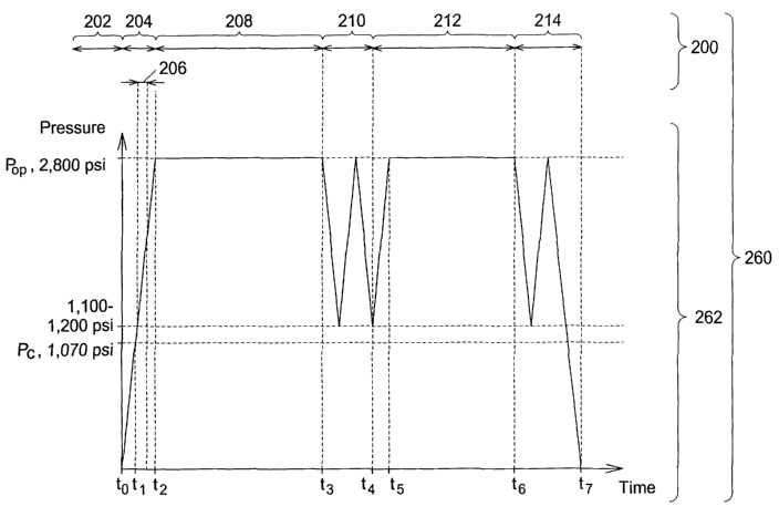
The preferred timeline of the present invention is graphically illustrated in
FIG.
8. The preferred timeline 260 indicates the preferred method 200 as a function
of time
and also indicates pressure 262 as a function of the time. It will be readily
apparent to
one skilled in the art that the time axis in FIG. 8 is only illustrative and
as such does not
indicate relative time periods to scale. Ideally, of course, all times would
be minimized
within reason to obtain an economical and efficient processing method.
Prior to an initial time to, the wafer is placed within the pressure chamber
226
and the pressure chamber is sealed in the first process step 202. From the
initial time to
through a first time t, to a second time t2, the pressure chamber 226 is
pressurized in the
second process step 204. The pressure chamber reaches critical pressure P~ at
the first
time t,. The critical pressure P~ for the supercritical carbon dioxide is
1,070 psi.
Preferably, the amine and the solvent are injected into the pressure chamber
226
between the first time t, and the second time t~ in the third process step
206. Preferably,
an amine and solvent injection begins upon reaching about 1100-1200 psi.
Alternatively, the amine and the solvent are injected into the pressure
chamber around
the second time t2 or after the second time t2. The pressure chamber reaches
an
operating pressure Pop at the second time t2. Preferably, the operating
pressure PoP is
-9-
CA 02387334 2002-04-11
WO 01/33613 PCT/US00/30218
about 2,800 psi. Alternatively, the operating pressure PoP is within the range
of from
1,070 psi to about 6,000 psi.
The preferred timeline 260 continues in the fourth process step 208 with
maintaining the supercritical carbon dioxide, the amine, and the solvent in
contact with
the wafer until the photoresist and the residue are removed from the wafer,
which takes
place from the second time t2 to a third time t3. In the fifth process step
210, the
pressure chamber 226 is partially exhausted from the third time t; to a fourth
time t4.
Preferably, this is accomplished by dropping from the operating pressure PoP
to about
the 1,100-1,200 psi in a first exhaust, raising from the 1,100-1,200 psi to
the operating
pressure PoP in a first pressure recharge, and dropping again to the 1,100-
1,200 psi in a
second exhaust. Alternatively, the pressure recharge and the second exhaust
are not
performed as part of the fifth process step 210. Further alternatively,
additional
recharges and exhausts are performed as part of the fifth process step 210
where one or
more of the exhausts can be a full exhaust.
The preferred timeline 260 continues in the sixth process step 212 with
rinsing
of the wafer from the fourth time t, through a fifth time t5 to a sixth time
t~,. The sixth
process step 212 begins with a second pressure recharge during which the rinse
agent is
preferably injected into the pressure chamber 226 from the fourth time t4 to
the fifth
time t5. In the seventh process step 214, the pressure chamber 226 is
exhausted from
the sixth time t~ to a seventh time t,. Preferably, this is accomplished by
dropping the
operating pressure P~P to about the 1,100-1,200 psi in a third exhaust,
raising from the
1,100-1,200 psi to the operating pressure PoP in a third pressure recharge,
and finally
dropping to atmospheric pressure in a final exhaust. Alternatively, the third
exhaust
and the third pressure recharge are not performed as part of the seventh
process step
214. Further alternatively, additional exhausts and recharges are performed as
part of
the seventh process step 210.
A first alternative embodiment of the present invention adds an aqueous
fluoride
to the preferred embodiment. In the first alternative embodiment, the
supercritical
carbon dioxide, the amine, the solvent, and the aqueous fluoride remove the
photoresist
and the residue. Preferably, the aqueous fluoride is selected from the group
of fluoride
bases and fluoride acids. More preferably, the aqueous fluoride is selected
from the
group consisting of aqueous ammonium fluoride (aqueous NH4F), and aqueous
hydrofluoric acid (HF).
The first alternative embodiment is useful when at least a portion of the
photoresist or a portion of the residue is removed from a silicon dioxide
(SiO~) surface.
The aqueous fluoride undercuts the Si02 surface from the photoresist and the
residue by
slightly etching the SiO~ surface. While the aqueous fluoride is useful in
removing the
photoresist or the residue form the Si02 surface of the wafer, the aqueous
fluoride
cannot be used when the wafer includes an exposed aluminum layer. This is
because
the aqueous fluoride will rapidly etch the exposed aluminum layer.
-10-
CA 02387334 2002-04-11
WO 01/33613 PCT/US00/30218
A second alternative embodiment of the present invention adds additional water
to the first alternative embodiment. The additional water enhances the first
alternative
embodiment because the photoresist is hydrophillic while the Si02 surface is
hydrophobic. Thus, the additional water separates the photoresist from the
SiOz
surface.
A third alternative embodiment of the present invention uses the supercritical
carbon dioxide and the aqueous fluoride to remove the photoresist and residue.
In the
third alternative embodiment, the amine is not used and the solvent is not
used.
A fourth alternative embodiment of the present invention adds the additional
water to the supercritical carbon dioxide and the aqueous fluoride.
A fifth alternative embodiment of the present invention adds the solvent to
the
third alternative embodiment.
In a first alternative timeline, the fourth process step 208 is performed at
an
initial cleaning pressure and a final cleaning pressure. Preferably, the
initial cleaning
IS pressure is about the 1,100-1,200 psi and the final cleaning pressure is
about the 2,800
psi. At the initial cleaning pressure, a first solubility of some of the
chemicals is lower
than a second solubility at the final cleaning pressure. During an initial
cleaning phase
which takes place at the initial cleaning pressure, lower solubility chemicals
condense
on the wafer. This provides greater concentration of the lower solubility
chemicals on
the photoresist and the residue and, thus, enhances separation of the
photoresist and the
residue from the wafer. During a final cleaning phase which takes place at the
final
cleaning pressure, the lower solubility chemicals either no longer condense or
condense
less on the wafer and, thus, concentration of the lower solubility chemicals
on the wafer
is reduced in anticipation of finishing the fourth process step 208.
In a second alternative timeline of the present invention, a second rinse is
performed after performing the first rinse.
Specific Embodiments
First through seventh specific embodiments of the present invention are
discussed below. Each of the first through seventh specific embodiments is a
summary
of a specific chemistry and a specific method employed in a lab system,
similar to the
preferred supercritical processing system 220. The lab system was used to
remove the
photoresist, or to remove the photoresist and the residue, or to remove the
residue from
test wafers. The lab system featured a combined internal volume for the
pressure
chamber 226, the circulation pump 230, and the circulation line 242 of about
1.8 liters.
The first through seventh specific embodiments were performed as part of a
proof of
concept feasibility study intended to show feasibility of the present
invention for use in
semiconductor fabrication. Before an incorporation of the present invention in
the
semiconductor fabrication, it is envisioned that further process refinements
would be
made.
-11-
CA 02387334 2002-04-11
WO 01/33613 PCT/US00/30218
First Specific Embodiment
In the first specific embodiment were removed from an SiO, via structure
formed in a preceding via etching step, where the etching step ended upon
reaching an
aluminum etch stop. The specific chemistry employed was as follows: 2 ml of 2-
methyl amino ethanol (the amine), 20 ml of DMSO (a first component of the
solvent),
and 20 ml of EC (a second component of the solvent). The pressure chamber was
maintained at 50 °C. The amine and the solvent were circulated for 5
minutes at 2,800
psi. Two partial exhausts and one full exhaust were employed between the
removal and
rinse steps in which the pressure was dropped from the 2,700 psi to 1,100 psi
for the
partial exhausts and the pressure was dropped from 2,700 psi to atmospheric
pressure in
the full exhaust. The rinse agent for the rinse step was 56 ml of the acetone.
The rinse
agent and the supercritical carbon dioxide were circulated for S minutes. One
partial
exhaust was performed prior to performing a complete exhaust following the
rinse step.
A first SEM photo was taken subsequent to removal of the photoresist and the
residue in the first specific embodiment. The first SEM photo showed that the
photoresist and the residue were removed in the first specific embodiment.
Second Specific Embodiment
In the second specific embodiment, the residue, including the photoresist
residue and the etch residue, was removed from a metal line structure formed
in a
preceding metal line etching step, where the etching step ended upon reaching
an oxide
etch stop. (The test wafer for the second specific embodiment was provided
courtesy of
Lucent Technologies.) The specific chemistry employed was as follows: 1.5 ml
of
PMDETA (the amine), 7.5 ml of NMP (the first component of the solvent), and 6
ml of
acetyl acetone (the second component of the solvent). The pressure chamber was
maintained at 50 °C. The amine and the solvent were circulated for 2
minutes at 2,800
psi. One partial exhaust and one full exhaust were employed between the
removal and
the rinse steps. The rinse agent for the rinse step was 20 ml of an 80%
ethanol and 20%
water mixture, by volume. The rinse agent and the supercritical carbon dioxide
were
circulated for 1 minute. A complete exhaust was performed following the rinse
step.
A second SEM photo was taken prior to removal of the residue in the second
specific embodiment. The second SEM photo showed the residue on sidewalk of
metal
lines, showed skirts of the residue protruding above the metal lines, and
showed the
residue remaining on tops of the metal lines. Third and fourth SEM photos were
taken
subsequent to removal of the residue in the second specific embodiment. The
third and
fourth SEM photos showed that the residue was removed in the second specific
embodiment.
Third Specific Embodiment
-12-
WO 01/33613 CA 02387334 2002-04-11 pCT~S00/30218
In the third specific embodiment, the photoresist was removed from a wafer
following a medium dose ion implant. The specific chemistry employed was as
follows: 0.15 ml of 24 % by volume aqueous ammonium fluoride (the aqueous
fluoride), 20 ml of BLO (the first component of the solvent), 20 ml of DMSO
(the
second component of the solvent), 0.15 ml of glacial acetic acid (a third
component of
the solvent), and 1 ml of additional water. The pressure chamber was
maintained at 70
°C. The aqueous fluoride and the solvent were circulated for 2 minutes
at 1,250 psi
after which the pressure chamber was pressurized to 2,800 psi. Two partial
exhausts
and one full exhaust were employed between the removal and rinse steps in
which the
pressure was dropped from the 2,700 psi to 1,100 psi for the partial exhausts
and the
pressure was dropped from 2,700 psi to atmospheric pressure in the full
exhaust. The
rinse agent for the rinse step was 20 ml of a mixture of 80% ethanol and 20%
water.
The rinse agent and the supercritical carbon dioxide were circulated for 1
minute. One
partial exhaust was performed prior to performing a complete exhaust following
the
rinse step.
Before and after XPS (x-ray photoelectron spectroscopy) tests demonstrated
that
the photoresist was removed in the third specific embodiment.
Fourth Specific Embodiment
In the fourth specific embodiment, the photoresist was removed from a wafer
following a high dose ion implant. The specific chemistry employed was as
follows:
0.22 ml of 24 % by volume aqueous ammonium fluoride (the aqueous fluoride), 20
ml
of DMSO (a first component of the solvent), 20 ml of EC (a second component of
the
solvent), and 2 ml of the additional water. The pressure chamber was
maintained at 70
°C. The aqueous fluoride and the solvent were circulated for 2 minutes
at 2,800 psi.
Two partial exhausts and one full exhaust were employed between the removal
and
rinse steps in which the pressure was dropped from the 2,700 psi to 1,100 psi
for the
partial exhausts and the pressure was dropped from 2,700 psi to atmospheric
pressure in
the full exhaust. The rinse agent for the rinse step was 20 ml of a mixture of
80%
ethanol and 20% water. The rinse agent and the supercritical carbon dioxide
were
circulated for 1 minute. One partial exhaust was performed prior to performing
a
complete exhaust following the rinse step.
Before and after XPS tests demonstrated that the photoresist was removed in
the
fourth specific embodiment.
Fifth Specific Embodiment
In the fifth specific embodiment, the photoresist was removed from an Si02 via
structure formed in a preceding via etching step, where the etching step ended
upon
reaching a TiN etch stop. The specific chemistry employed was as follows: 0.15
ml of
24 % by volume aqueous ammonium fluoride (the aqueous fluoride) and 8 ml of
-13-
WO 01/33613 CA 02387334 2002-04-11 pCT~S00/30218
additional water. The pressure chamber was maintained at 50 °C. The
aqueous fluoride
and the additional water were circulated for 2 minutes at 1,500 psi. Two
partial
exhausts and one full exhaust were employed between the removal step and the
first
rinse step in which the pressure was dropped from the 1,500 psi to 1,050 psi
for the
S partial exhausts and the pressure was dropped from 1,500 psi to atmospheric
pressure in
the full exhaust. The rinse agent for the first rinse step was 12 ml of water.
In the first
rinse step, the rinse agent and the supercritical carbon dioxide were
circulated for 1
minute at 1,500 psi following which the pressure was raised to 2,800 psi. Two
partial
exhausts and one full exhaust were employed between the first rinse step and
the
second rinse step in which the pressure was dropped from the 2,800 psi to
1,100 psi for
the partial exhausts and the pressure was dropped from2,800 psi to atmospheric
pressure in the full exhaust. The rinse agent for the second rinse was 20 ml
of
methanol. In the second rinse step, the rinse agent and the supercritical
carbon dioxide
were circulated for 1 minute at the 2,800 psi. One partial exhaust was
performed prior
to performing a complete exhaust following the second rinse step.
A fifth SEM photo was taken prior to removal of the photoresist in the fifth
specific embodiment. The fifth SEM photo showed the photoresist above the SiOz
via
structure and the TiN etch stop at a bottom of the via. A sixth SEM photo was
taken
subsequent to removal of the photoresist in the fifth specific embodiment. The
sixth
SEM photo showed that the photoresist was removed in the fifth specific
embodiment.
Sixth Specific Embodiment
In the sixth specific embodiment, the photoresist was removed from an SiO~ via
structure formed in a preceding via etching step. The specific chemistry
employed was
as follows: 1.5 ml of 24 % by volume aqueous ammonium fluoride (the aqueous
fluoride), and 8 ml of DMSO (the solvent) and 4 ml of additional water. The
pressure
chamber was maintained at 50 °C. The aqueous fluoride, the solvent, and
the additional
water were circulated for 2 minutes at 2,800 psi. One partial exhaust and one
full
exhaust were employed between the removal step and the rinse step. The rinse
agent
was 20 ml of 80 % ethanol and 20% water. The rinse agent and the supercritical
carbon
dioxide were circulated for 1 minute at 2,700 psi. One partial exhaust was
performed
prior to performing a complete exhaust following the rinse step.
A seventh SEM photo was taken subsequent to removal of the photoresist in the
sixth specific embodiment. The seventh SEM photo showed that the photoresist
was
removed in the sixth specific embodiment.
Seventh Specific Embodiment
In the seventh specific embodiment, the photoresist and the residue were
removed from a C-SiO~ damascene structure formed in a preceding via etching
step.
The specific chemistry employed was as follows: 0.1 S ml of 24 % by volume
aqueous
- 14-
CA 02387334 2002-04-11
WO 01/33613 PCT/US00/30218
ammonium fluoride (the aqueous fluoride), 20 ml of BLO (the first component of
the
solvent), 20 ml of DMSO (the second component of the solvent), 0.1 S ml of
glacial
acetic acid (the third component of the solvent), and 1 ml of additional
water. The
pressure chamber was maintained at 70 °C. The aqueous fluoride, the
solvent, and the
additional water were circulated for 2 minutes at 2,800 psi. Two partial
exhausts and
one full exhaust were employed between the removal step and the rinse step.
The rinse
agent for the rinse step was 20 ml of SO % ethanol and 50% water. The rinse
agent and
the supercritical carbon dioxide were circulated for 1 minute at 2,700 psi.
One partial
exhaust was performed prior to performing a complete exhaust following the
rinse step.
An eighth SEM photo was taken subsequent to removal of the photoresist and
residue in the seventh specific embodiment. The eighth SEM photo showed that
the
photoresist and the residue were removed in the seventh specific embodiment.
It will be readily apparent to one skilled in the art that other various
modifications may be made to the preferred embodiment without departing from
the
spirit and scope of the invention as defined by the appended claims.
-15-